Fabrication Development for SPT-SLIM, a Superconducting Spectrometer for Line Intensity Mapping
Abstract
Line Intensity Mapping (LIM) is a new observational technique that uses low-resolution observations of line emission to efficiently trace the large-scale structure of the Universe out to high redshift. Common mm/sub-mm emission lines are accessible from ground-based observatories, and the requirements on the detectors for LIM at mm-wavelengths are well matched to the capabilities of large-format arrays of superconducting sensors. We describe the development of an = on-chip superconducting filter-bank spectrometer covering the 120–180 GHz band for future mm-LIM experiments, focusing on SPT-SLIM, a pathfinder LIM instrument for the South Pole Telescope. Radiation is coupled from the telescope optical system to the spectrometer chip via an array of feedhorn-coupled orthomode transducers. Superconducting microstrip transmission lines then carry the signal to an array of channelizing half-wavelength resonators, and the output of each spectral channel is sensed by a lumped element kinetic inductance detector (leKID). Key areas of development include incorporating new low-loss dielectrics to improve both the achievable spectral resolution and optical efficiency and development of a robust fabrication process to create a galvanic connection between ultra-pure superconducting thin-films to realize multi-material (hybrid) leKIDs. We provide an overview of the spectrometer design, fabrication process, and prototype devices.
Index Terms:
Superconducting device fabrication, Microstrip Resonators, Millimeter wave detectors, Submillimeter wave detectors, Superconducting resonatorsI Introduction
Studies of the mm-wave sky have provided a wealth of information about the history of the universe. The cosmic microwave background (CMB) at a redshift of provides a window to the earliest stages of the universe as high-energy photons are redshifted down into the mm-wave band. Similarly, far-infrared photons in the later universe are redshifted into the mm-wave band. Line intensity mapping (LIM) is a technique that uses integrated line emissions to trace the large-scale structure of the Universe out to high redshift [1]. LIM techniques have the potential to constrain cosmology (e.g., inflation, dark energy, neutrino mass) with higher precision than CMB and galaxy surveys [2, 3, 4]. Many common mm/sub-mm emission lines are accessible from ground-based observatories, matching with atmospheric transmission windows. Additionally, the requirements for detectors in future LIM experiments are well aligned with existing capabilities achievable with large-format arrays of superconducting sensors [5]. Many early detector plans for LIM experiments [6, 7, 8] draw on the heritage from decades of CMB and leKID detector development incorporating features such as low-loss superconducting microstrips [9, 10] , othrho-mode transducer (OMT) optical coupling [11, 12], and leKIDs [13] to realize OMT coupled KIDs[14, 15, 16]. The combination of accessible mm/sub-mm emission lines and large-format arrays of superconducting sensors makes LIM experiments a promising pathway for future cosmological breakthroughs.
The spectrometer development described below is aimed at producing the focal plane for the planned South Pole Telescope Summertime Line Intensity Mapper (SPT-SLIM) experiment [17]. SPT-SLIM is a pathfinder LIM instrument for the South Pole Telescope. It is designed to use the same primary mirror as the SPT-3G experiment with new pickoff mirrors and a dedicated cryostat. The cryostat will be cooled to 100 mK through the combination of a pulse tube cryocooler and an adiabatic demagnetization refrigerator (ADR). The focal plane will be filled with 18 dual-polarization pixels, each coupled to an = microstrip spectrometer covering the 120–180 GHz band. Additional details on the spectrometer design are provided below in Section II. SPT-SLIM will be the first demonstration of on-chip spectroscopy in LIM-style observations that is sensitive to CO emission from . SPT-SLIM is scheduled to deploy to the South Pole for observations in the 2023–2024 austral summer.
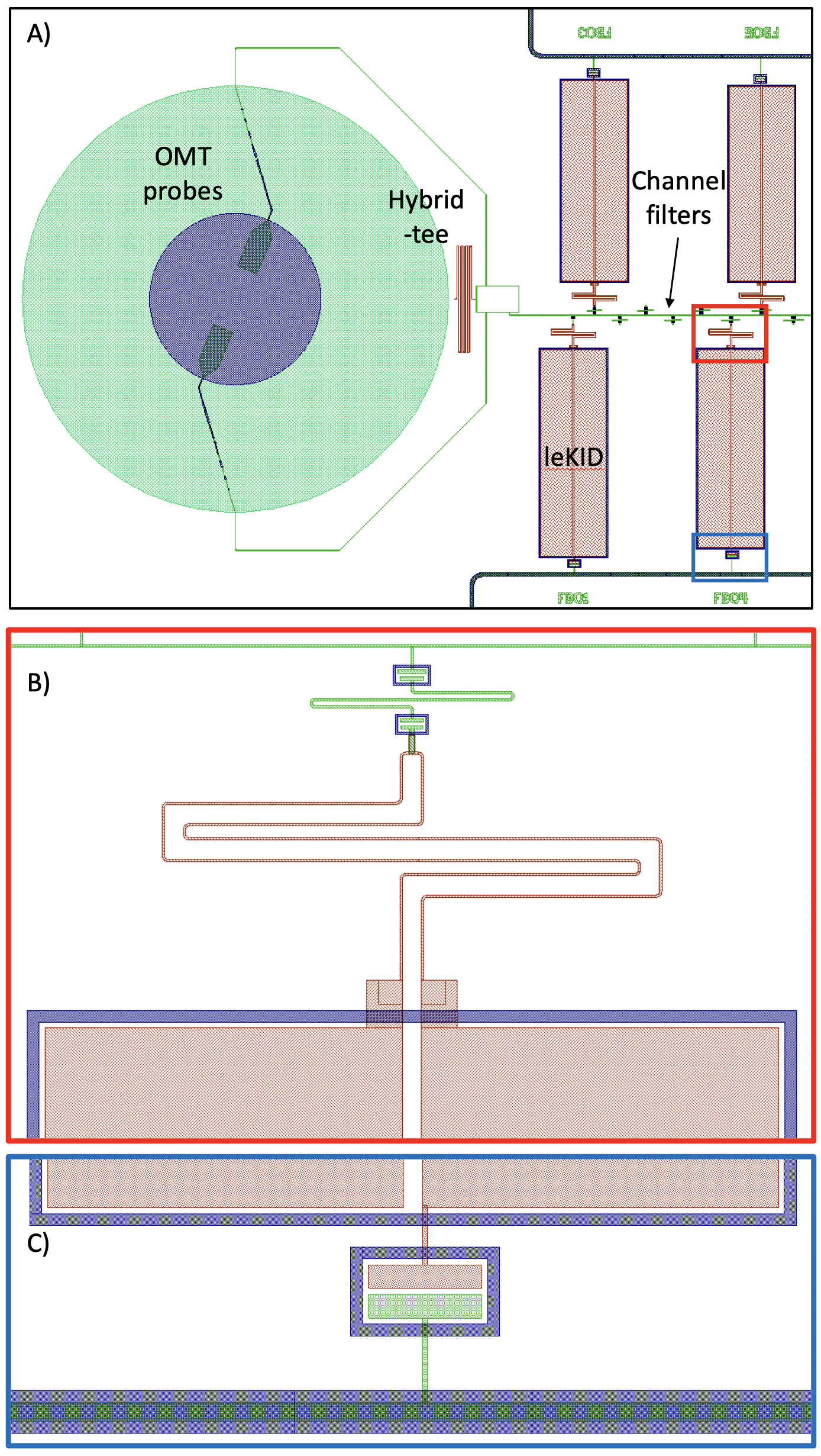
II Spectrometer design
SPT-SLIM employs filterbank-style spectrometers [18, 19]. The key components for the spectrometer are shown in Figure 1. Optical signals from the telescope are coupled to the spectrometer via a feedhorn to an ortho-mode transducer (OMT) coupling. The signal from opposing OMT probes are combined in a hybrid-tee and the resulting signal continues down a microstrip transmission line. For each filter bank channel one end of a channelizing resonator is capacitively coupled to the microstrip feedline, with each filter picking off a narrow frequency band. The channel filters are arranged from high to low frequency along the feedline with the higher-frequency channels closer to the hybrid-tee. The channel filters are designed to oversample the 120–180 GHz band. The other end of the channelizing resonator is capacitively coupled to the inductor of a lumped element kinetic inductance detector (leKID) that is used to detect the power in each channel and provides readout multiplexing. The capacitor of the leKID is capacitively coupled to a co-planar waveguide that serves as the readout line. The leKIDs are designed to resonate at GHz with a frequency spacing of 500 kHz between each resonance. The frequency range was selected to match the chosen readout hardware [20] and balance the trade-off between lower resonance frequencies and larger resonator size.
III Fabrication process
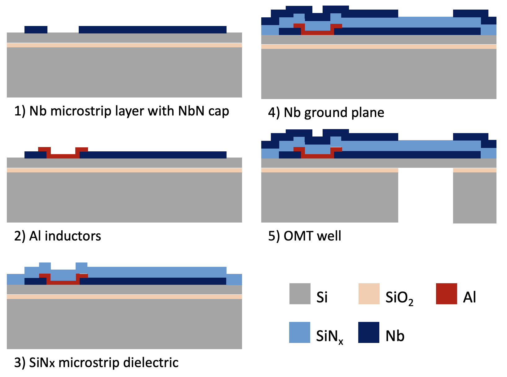
Spectrometer fabrication was carried out at the Center for Nanoscale Materials at Argonne National Laboratory. The superconducting microstrip and capacitors of the readout leKID are made from a Nb-NbN/dielectric/Nb stack that uses a silicon-based dielectric as described in Section III-A. The readout leKID is a hybrid device that pairs the Nb capacitors to an Al inductor. A NbN cap layer is grown on the top of the bottom Nb layer to provide a galvanic contact to the Al inductor as described in Section III-B. Nb was used in the capacitors both due to reports of lower two-level systems (TLS) noise levels for Nb grown on Si as compared to Al on Si [21] and to boost the effective kinetic inductance fraction by minimizing additional kinetic inductance from the capacitor.
The process flow to fabricate the filter bank spectrometer is shown in Figure 2. The spectrometer begins with a silicon on insulator wafer (SOI) with a high-resistivity device layer ( kOhm-cm) to limit losses from the substrate. The spectrometer design uses an inverted microstrip layout; using this geometry reduces the number of processing steps prior to the deposition of the Al inductors and deposits the Al layer on the high-resistivity silicon substrate in an effort to yield the highest quality Al film. The first layer is the spectrometer wiring including OMT probes, transmission lines, channelizing filters, and leKID capacitors. This layer consists of 170 nm thick Nb with a 30 nm thick NbN capping layer, which is used to form a galvanic contact to the Al inductor (for additional details on the NbN capping layer see Section III-B). The Nb/NbN layer is patterned using a fluorine-based reactive ion etch. Next the 30 nm Al inductors are patterned using a bilayer liftoff process. The Al thickness is chosen based upon the inductor volume to achieve the required responsivity for the expected optical loading from the South Pole [18]. Following the wiring layers is the dielectric layer. The current baseline is a Si-rich SiNx deposited by plasma-enhanced chemical vapor deposition (PECVD) at a temperature of 100∘C to avoid damaging the Al inductors. After the dielectric, the Nb ground plane is deposited and patterned via liftoff. Using a liftoff process avoids any shorting that could occur from material that is deposited on the sidewall of steps; sidewall material may not be removed by an anisotropic reactive ion etch process. Next, the OMT membrane is formed by a deep reactive ion etch (DRIE) from the back side of the wafer to remove the SOI handle wafer from behind the OMT probes. Lastly, a wet etch with 10 HF buffered oxide etch is used to remove the buried oxide layer in the OMT well.
Realization of this fabrication process required addressing key technical challenges which are addressed in more detail below. The first key challenge was identifying a low-temperature dielectric deposition process that yields a low-loss dielectric. The second challenge was achieving a robust galvanic contact between the Al and Nb layers in the hybrid leKIDS despite the presence of native oxides. The last challenge seeks an alternative substrate to SOI wafers. Although high quality leKIDs have been fabricated on SOI [22] the increased cost and lead time for SOI wafers with high-resistivity device layers makes them difficult to work with in a development project where detector designs are still iterating. We explore an alternate substrate using isolated SiNx membranes.
III-A Low-loss Dielectrics
The quality of the dielectric used in the microstrip transmission lines and half wave channelizing filters plays a key role in the overall performance of the spectrometers. The dielectric loss tangent sets a practical limit on the spectrometer’s resolution by placing a lower limit on the channelizing filter bandwidth. It also impacts the overall filter efficiency. Previous work [19] simulating the performance of the SPT-SLIM filters targets a loss tangent of at mm-wave frequencies. From microstrip dielectric loss measurements we expect the loss tangent at mm-wave to be up to a factor of 10 higher than the loss tangent measured at microwave frequencies [Hähnle.2021] and thus seek a dielectric with a loss tangent near at microwave frequencies. A wide range of potential dielectrics are available with many of these achieving the desired loss tangent, e.g., SiNx [23, 9], amorphous silicon (a-Si) [Hähnle.2021] and amorphous silicon carbide (a-SiC) [24]. However, many of the deposition processes used for these high quality dielectrics involve heating the substrate to temperatures of several hundred degrees (C to 350∘C). This poses challenges for the inverted microstrip process. We have observed degradation to Al inductors - formation of hillocks - when heated above C and avoid any subsequent processing temperatures above this. We surveyed a range of different materials and deposition processes to identify a low-loss dielectric that can be deposited at low temperatures [25]. A summary of materials and processes used is shown in Table 1. The ideal dielectric will have low intrinsic stress, high thickness uniformity, and limited pin holes. a-Si deposited via chemical vapour deposition (CVD) meets many of these criteria, but requires substrate temperatures above 250∘C. Alternatives process with lower temperature requirements include PECVD and ion-beam assisted sputtering (IBAS). The IBAS process is especially attractive as it allows for room temperature depositions compatible with liftoff processing. After evaluating several films we have identified a Si-rich SiNx film deposited via PECVD that meets all the criteria for use with inverted microstrip. With a loss tangent of at microwave frequencies (1 GHz) this dielectric loss is the lowest of the evaluated dielectrics with a low-temperature process. Additional testing of the loss tangent at mm-wave frequencies will be needed to make sure the performance does not degrade at higher frequencies.
| Material | Process | Temp | Loss Tangent |
|---|---|---|---|
| (C) | ( 4 GHz) | ||
| SiN | CVD | 275 | 2E-3 |
| a-Si | CVD | 275 | 4E-5 |
| SiN | PECVD | 100 | 2E-3 |
| Si-rich SiN | PECVD | 100 | 2E-4 |
| SiO2 | IBAS | 20 | 8E-4 |
| SiN | IBAS | 20 | 2E-3 |
| Si-rich SiN | IBAS | 20 | 8E-4 |
| a-Si | IBAS | 20 | 5E-4 |
III-B Galvanic Contacts Using a NbN Interface Layer
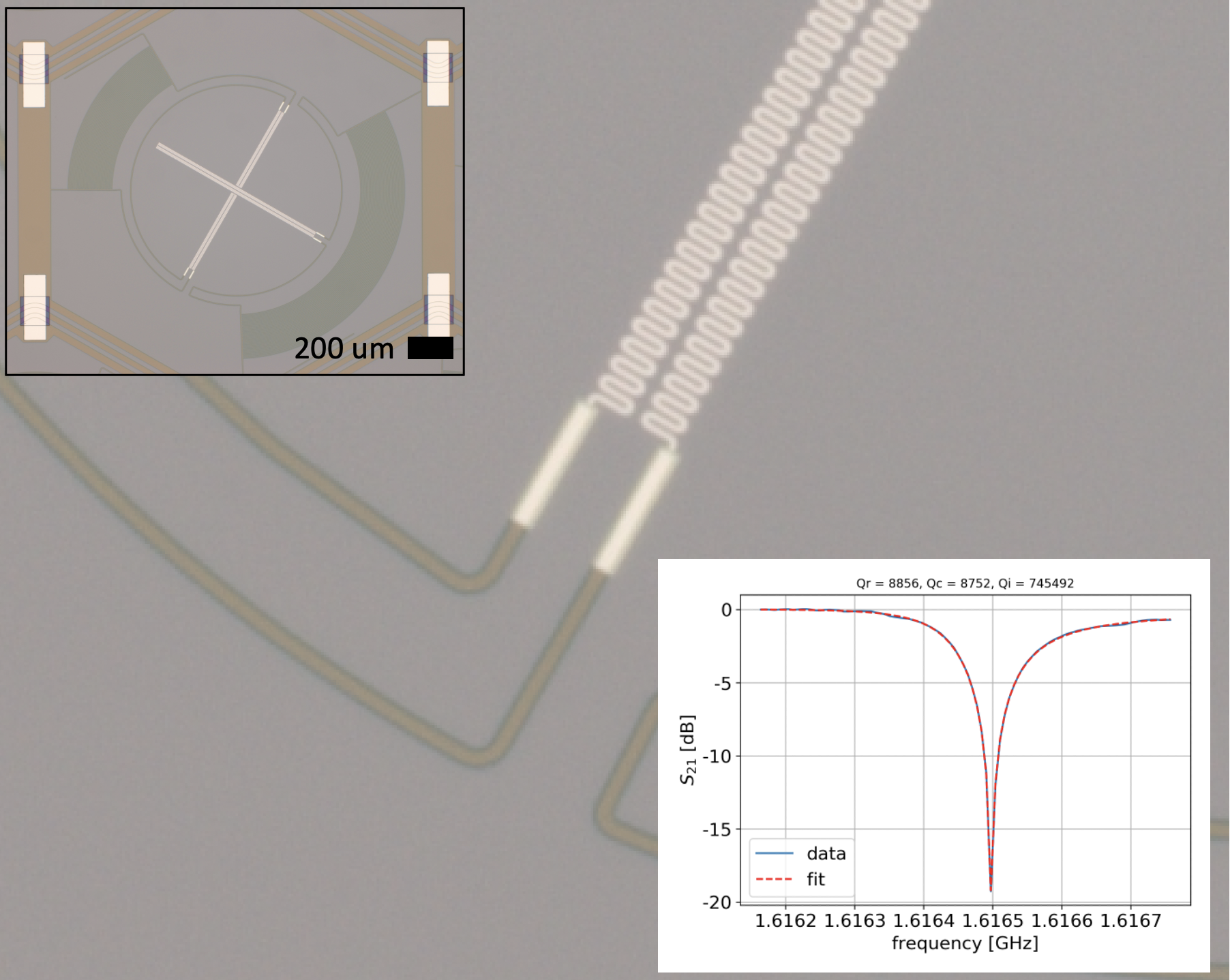
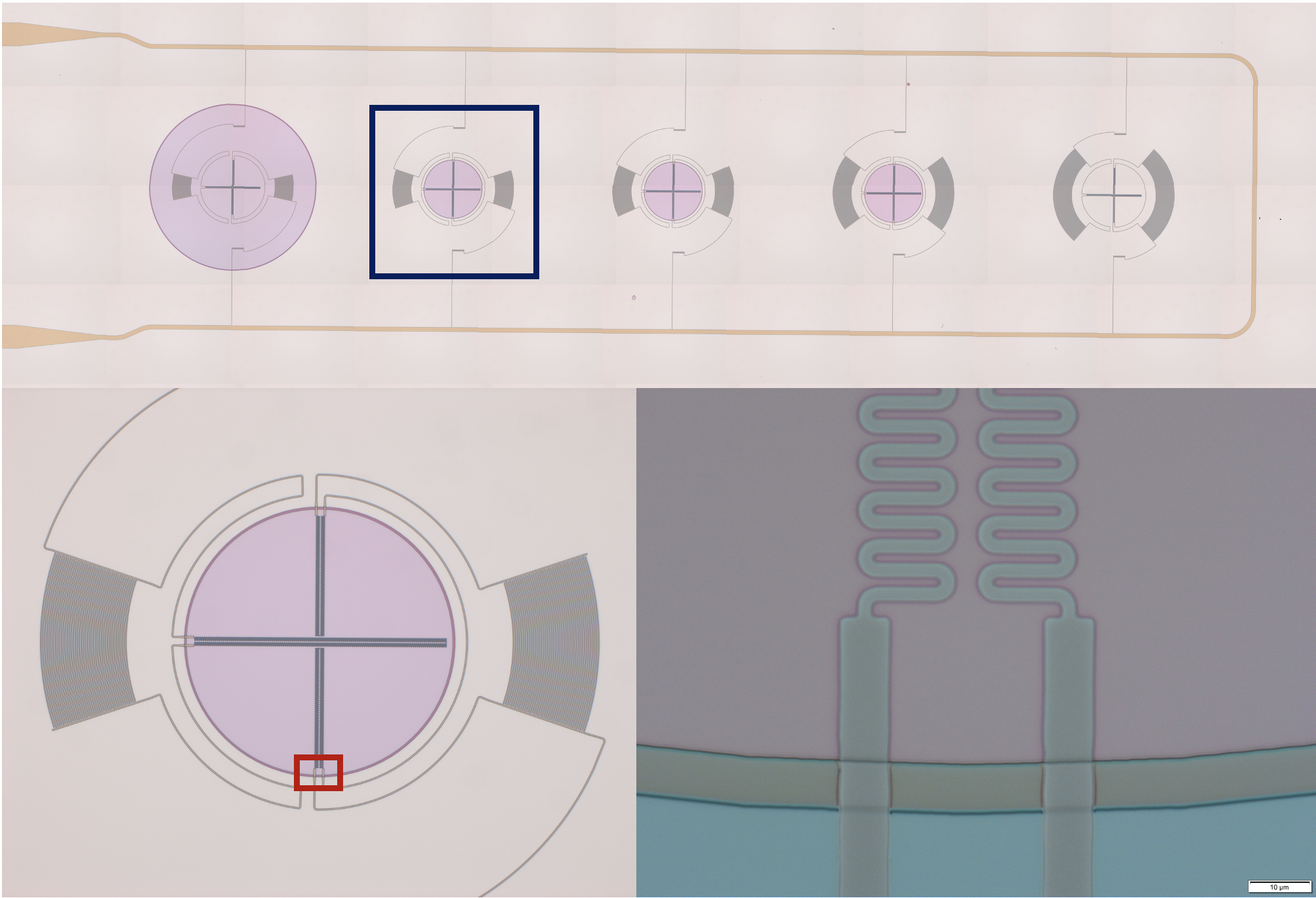
The hybrid structure of the kinetic inductance detectors—Al inductors and Nb capacitors—poses an additional fabrication challenge in ensuring a clean galvanic contact between the Al and Nb layers. Early attempts at fabricating inverted microstrip devices deposited the Al inductors first followed by the Nb capactors. These devices showed inconsistent contact between the layers with some devices open and others with various level of contact resistance. The deposition system at Argonne does not have an ion mill, but historically has used an RF substrate bias to clean surfaces prior to deposition. This cleaning step proved insufficient in removing the native aluminum oxide from the inductors prior to the subsequent Nb deposition. Similar devices fabricated at the University of Chicago using an ion mill were sensitive to the ion mill settings and also yielded inconsistent contact between the layers. To provide a clean galvanic contact between the layers, the process steps were flipped with the Nb deposited first and a thin ( nm) NbN capping layer added to the top of the Nb. The NbN cap limits oxidation of the Nb when the Nb layer is removed from vacuum and patterned. Both DC and RF test structures have been fabricated to evaluate the performance of the cap layer. The DC test structures consist of a pair of Nb-NbN-Al-NbN-Nb connections with various contact geometries. The measured resistance of the DC test structures dropped to zero when below the Al transition temperature with no sign of an interface resistance. To verify the performance at microwave frequencies we fabricated leKIDs using an SPT-3G+ design we have previously characterized and shown to have high quality factors [26, 27]. A photo of one such device along with a trace of for an example resonator are shown in Figure 3. Hybrid leKIDS made using the NbN capping layer demonstrated high internal quality factors, indicating the NbN layer was not degrading device performance.
III-C Membrane Step Down
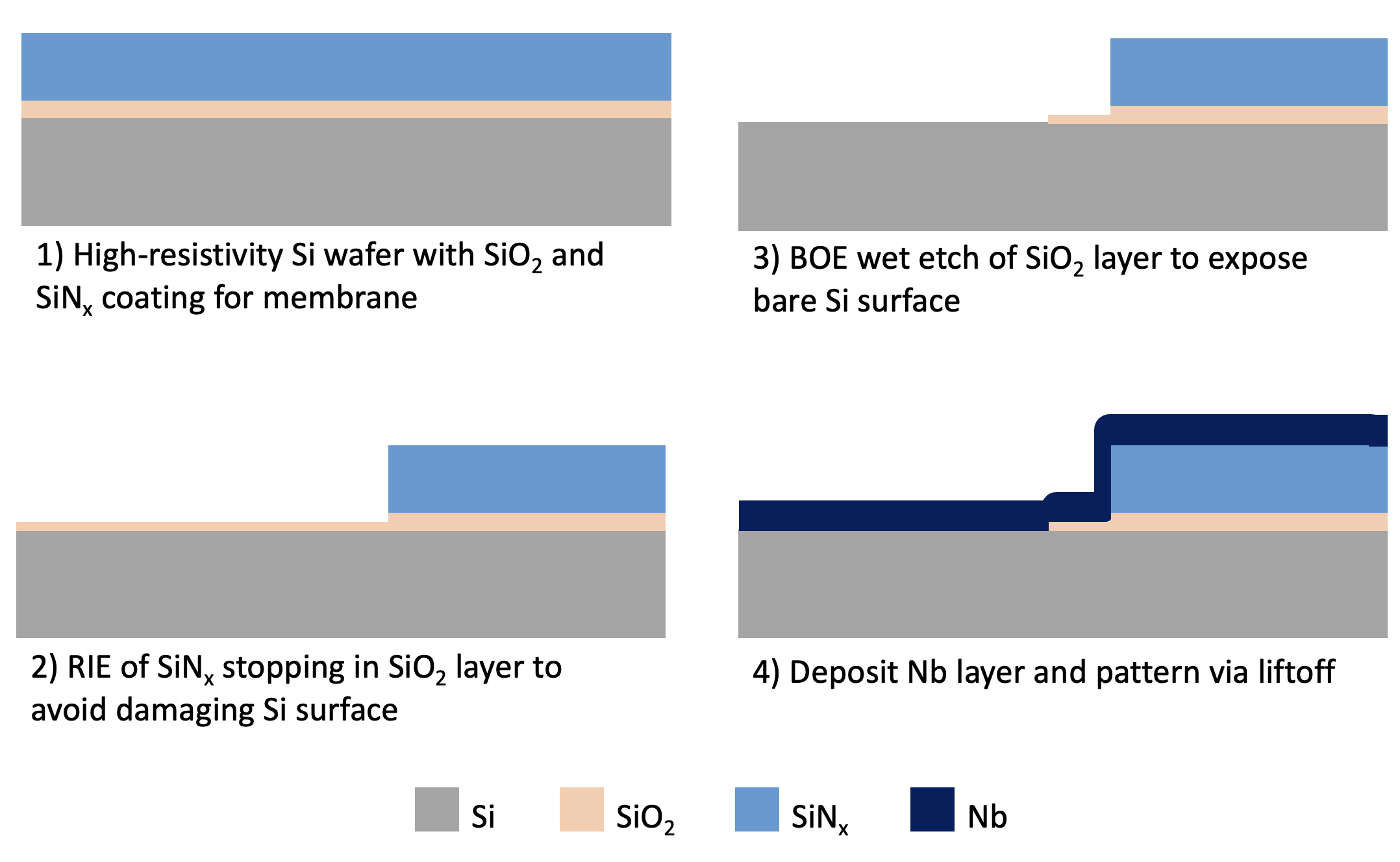
The baseline design for SPT-SLIM calls for the spectrometers to be fabricated on a silicon on insulator (SOI) wafer with a high-resistivity device layer. This provides a high-quality surface on which to deposit the inverted microstrip layers. However, SOI wafers can be significantly more expensive than bulk wafers and can have long lead times when requiring specific device layer properties (e.g., thickness and resistivity). As an alternative we are exploring using bulk high-resistivity Si wafers coated with thin SiO2 and SiNx layers. The SiO2/SiNx layers are used to create a membrane for the OMT probes [28]. But these amorphous dielectric layers are expected to degrade the noise performance of the resonators by introducing an additional source of TLS [21]. To reduce the presence of TLS in the vicinity of the mm-wave components, we have developed a process for removing the majority of these dielectrics from the wafer. A cartoon cross section of the process is shown in Figure 4. The first step is to lithographically pattern circles slightly larger than the diameter of the OMT probes. The SiNx layer is etched in a RIE with an optical end point detection system to ensure the etch stops in the SiO2 layer. The resist is stripped and a second lithography step is completed with a slightly larger diameter (roughly 10 m) than the SiNx pattern. The SiO2 layer is then etched in 10% HF buffered oxide etch to remove the SiO2, a common practice for reducing TLS for superconducting circuits. A final lithography step is performed to define the probe and wiring layer. The Nb wiring with a NbN cap layer is deposited and patterned via liftoff. Because material deposited with the sputtering process is not fully line-of-sight, the sidewalls of the membrane step are also coated with Nb providing a continuous film from the top of the membrane layer, over the sidewalls, and on to the bare silicon surface. DC connectivity tests demonstrated electrical connectivity of the Nb film over the step edge.
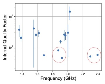
To fully characterize the stepdown process we have fabricated test arrays using the same well-characterized SPT-3G+ leKIDs described above that now incorporate different amounts of SiNx under the resonator. Photos of a representative chip are shown in Figure 5. There are three resonator types: resonators that sit entirely on the SiNx, resonators with inductors on the SiNx and capacitors on bare silicon, and resonators entirely on bare silicon. Figure 6 shows the internal quality factors for a similar chip with sixteen resonators: four entirely on SiNx, eight with inductors on the SiNx and capacitors on bare silicon, and four entirely on bare silicon. All sixteen resonators are present suggesting that the stepdown does not impact resonator yield. Based upon frequency scheduling we identify the resonators circled by the dashed line as those resonators entirely on SiNx, which also are among the lowest internal quality factors. Eleven of the twelve other resonators have internal quality factors greater than ; the cause of the 5th resonator with low internal quality factor is unclear. Following quality factor measurements, the next step for this test is to measure the noise performance.
IV Prototype Chips
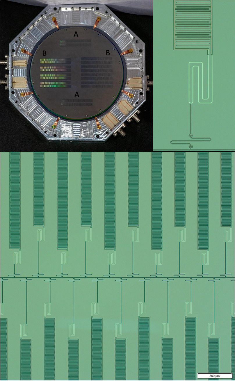
Prototype chips to test isolated components of the spectrometer are in development. A layout for this chip is shown in Figure 7. The layout consists of four sets of spectrometer-like devices (optical coupling structures have been left out to simplify the fabrication process). Two of the devices consist of four readout banks, each bank containing 194 leKID channels with the entire device spanning 2.011–2.489 GHz; the 500 kHz resonator spacing is the targeted spacing for the final SLIM instrument. Two of the devices have sparse spacing with 194 leKIDs spanning the entire 500 MHz readout bandwidth. Fabrication of these devices is currently ongoing.
Following testing of the isolated components several steps of integrated testing are required on the path to a deployable focal plane. This testing will be done using a layout that combines a series of test chips and a spectrometer sub-module on a single wafer. Fabrication and testing rounds are needed to verify our resonator trimming process, the optical pass bands, and the microstrip transmission loss at mm-wave for the selected dielectric, which is still to be determined. By combining test chips and sub-modules on a single wafer, once testing verifies a successful fabrication process we will have a potentially deployable portion of the focal plane in hand. Design and layout of these wafers is ongoing.
V Conclusions
Line Intensity Mapping is a promising experimental technique for uncovering answers to some of the most fundamental questions about the nature of the universe. Superconducting spectrometers operating in the mm-wave frequency band are well matched to the needs of future mm-wave LIM experiments. We describe the development of superconducting spectrometers designed to operate in the 120–180 GHz band for the upcoming SPT-SLIM instrument which is scheduled to deploy in the 2023–2024 austral summer. This instrument will serve as a pathfinder to demonstrate the viability of ground-based LIM measurements in the mm-wave bands.
References
- [1] E. D. Kovetz, M. P. Viero, A. Lidz, L. Newburgh, M. Rahman, E. Switzer, M. Kamionkowski, J. Aguirre, M. Alvarez, J. Bock, J. R. Bond, G. Bower, C. M. Bradford, P. C. Breysse, P. Bull, T.-C. Chang, Y.-T. Cheng, D. Chung, K. Cleary, A. Corray, A. Crites, R. Croft, O. Doré, M. Eastwood, A. Ferrara, J. Fonseca, D. Jacobs, G. K. Keating, G. Lagache, G. Lakhlani, A. Liu, K. Moodley, N. Murray, A. Pénin, G. Popping, A. Pullen, D. Reichers, S. Saito, B. Saliwanchik, M. Santos, R. Somerville, G. Stacey, G. Stein, F. Villaescusa-Navarro, E. Visbal, A. Weltman, L. Wolz, and M. Zemcov, “Line-Intensity Mapping: 2017 Status Report,” arXiv e-prints, p. arXiv:1709.09066, Sep. 2017.
- [2] A. Moradinezhad Dizgah and G. K. Keating, “Line Intensity Mapping with [C II] and CO(1-0) as Probes of Primordial Non-Gaussianity,” The Astrophysical Journal, vol. 872, no. 2, p. 126, Feb. 2019.
- [3] K. S. Karkare and S. Bird, “Constraining the expansion history and early dark energy with line intensity mapping,” Physical Rreview D, vol. 98, no. 4, p. 043529, Aug. 2018.
- [4] A. Moradinezhad Dizgah, G. K. Keating, K. S. Karkare, A. Crites, and S. R. Choudhury, “Neutrino Properties with Ground-based Millimeter-wavelength Line Intensity Mapping,” The Astrophysical Journal, vol. 926, no. 2, p. 137, Feb. 2022.
- [5] K. S. Karkare, A. M. Dizgah, G. K. Keating, P. Breysse, and D. T. Chung, “Snowmass 2021 Cosmic Frontier White Paper: Cosmology with Millimeter-Wave Line Intensity Mapping,” arXiv, 2022.
- [6] A. Endo, J. J. A. Baselmans, P. P. v. d. Werf, B. Knoors, S. M. H. Javadzadeh, S. J. C. Yates, D. J. Thoen, L. Ferrari, A. M. Baryshev, Y. J. Y. Lankwarden, P. J. d. Visser, R. M. J. Janssen, and T. M. Klapwijk, “Development of DESHIMA: a redshift machine based on a superconducting on-chip filterbank,” Millimeter, Submillimeter, and Far-Infrared Detectors and Instrumentation for Astronomy VI, pp. 84 520X–84 520X–15, 2012.
- [7] E. Shirokoff, P. S. Barry, C. M. Bradford, G. Chattopadhyay, P. Day, S. Doyle, S. Hailey-Dunsheath, M. I. Hollister, A. Kovács, H. G. Leduc, C. M. McKenney, P. Mauskopf, H. T. Nguyen, R. O’Brient, S. Padin, T. J. Reck, L. J. Swenson, C. E. Tucker, and J. Zmuidzinas, “Design and Performance of SuperSpec: An On-Chip, KID-Based, mm-Wavelength Spectrometer,” Journal of Low Temperature Physics, vol. 176, no. 5-6, pp. 657–662, 2014.
- [8] G. Cataldo, E. M. Barrentine, B. T. Bulcha, N. Ehsan, L. A. Hess, O. Noroozian, T. R. Stevenson, E. J. Wollack, S. H. Moseley, and E. R. Switzer, “Second-generation Micro-Spec: A compact spectrometer for far-infrared and submillimeter space missions,” Acta Astronautica, vol. 162, pp. 155–159, 2019.
- [9] S. M. Duff, J. Austermann, J. A. Beall, D. Becker, R. Datta, P. A. Gallardo, S. W. Henderson, G. C. Hilton, S. P. Ho, J. Hubmayr, B. J. Koopman, D. Li, J. McMahon, F. Nati, M. D. Niemack, C. G. Pappas, M. Salatino, B. L. Schmitt, S. M. Simon, S. T. Staggs, J. R. Stevens, J. V. Lanen, E. M. Vavagiakis, J. T. Ward, and E. J. Wollack, “Advanced ACTPol Multichroic Polarimeter Array Fabrication Process for 150 mm Wafers,” Journal of Low Temperature Physics, vol. 184, no. 3-4, pp. 634–641, 2016.
- [10] C. M. Posada, P. A. R. Ade, Z. Ahmed, K. Arnold, J. E. Austermann, A. N. Bender, L. E. Bleem, B. A. Benson, K. Byrum, J. E. Carlstrom, C. L. Chang, H. M. Cho, S. T. Ciocys, J. F. Cliche, T. M. Crawford, A. Cukierman, D. Czaplewski, J. Ding, R. Divan, T. d. Haan, M. A. Dobbs, D. Dutcher, W. Everett, A. Gilbert, N. W. Halverson, N. L. Harrington, K. Hattori, J. W. Henning, G. C. Hilton, W. L. Holzapfel, J. Hubmayr, K. D. Irwin, O. Jeong, R. Keisler, D. Kubik, C. L. Kuo, A. T. Lee, E. M. Leitch, S. Lendinez, S. S. Meyer, C. S. Miller, J. Montgomery, M. Myers, A. Nadolski, T. Natoli, H. Nguyen, V. Novosad, S. Padin, Z. Pan, J. Pearson, J. E. Ruhl, B. R. Saliwanchik, G. Smecher, J. T. Sayre, E. Shirokoff, L. Stan, A. A. Stark, J. Sobrin, K. Story, A. Suzuki, K. L. Thompson, C. Tucker, K. Vanderlinde, J. D. Vieira, G. Wang, N. Whitehorn, V. Yefremenko, K. W. Yoon, and K. E. Ziegler, “Fabrication of large dual-polarized multichroic TES bolometer arrays for CMB measurements with the SPT-3G camera,” Superconductor Science and Technology, vol. 28, no. 9, p. 094002, 2015.
- [11] S. W. Henderson, R. Allison, J. Austermann, T. Baildon, N. Battaglia, J. A. Beall, D. Becker, F. D. Bernardis, J. R. Bond, E. Calabrese, S. K. Choi, K. P. Coughlin, K. T. Crowley, R. Datta, M. J. Devlin, S. M. Duff, J. Dunkley, R. Dünner, A. v. Engelen, P. A. Gallardo, E. Grace, M. Hasselfield, F. Hills, G. C. Hilton, A. D. Hincks, R. Hlozek, S. P. Ho, J. Hubmayr, K. Huffenberger, J. P. Hughes, K. D. Irwin, B. J. Koopman, A. B. Kosowsky, D. Li, J. McMahon, C. Munson, F. Nati, L. Newburgh, M. D. Niemack, P. Niraula, L. A. Page, C. G. Pappas, M. Salatino, A. Schillaci, B. L. Schmitt, N. Sehgal, B. D. Sherwin, J. L. Sievers, S. M. Simon, D. N. Spergel, S. T. Staggs, J. R. Stevens, R. Thornton, J. V. Lanen, E. M. Vavagiakis, J. T. Ward, and E. J. Wollack, “Advanced ACTPol Cryogenic Detector Arrays and Readout,” Journal of Low Temperature Physics, vol. 184, no. 3-4, pp. 772–779, 2016.
- [12] N. Galitzki, A. Ali, K. S. Arnold, P. C. Ashton, J. E. Austermann, C. Baccigalupi, T. Baildon, D. Barron, J. A. Beall, S. Beckman, S. M. M. Bruno, S. Bryan, P. G. Calisse, G. E. Chesmore, Y. Chinone, S. K. Choi, G. Coppi, K. D. Crowley, K. T. Crowley, A. Cukierman, M. J. Devlin, S. Dicker, B. Dober, S. M. Duff, J. Dunkley, G. Fabbian, P. A. Gallardo, M. Gerbino, N. Goeckner-Wald, J. E. Golec, J. E. Gudmundsson, E. E. Healy, S. Henderson, C. A. Hill, G. C. Hilton, S.-P. P. Ho, L. A. Howe, J. Hubmayr, O. Jeong, B. Keating, B. J. Koopman, K. Kiuchi, A. Kusaka, J. Lashner, A. T. Lee, Y. Li, M. Limon, M. Lungu, F. Matsuda, P. D. Mauskopf, A. J. May, N. McCallum, J. McMahon, F. Nati, M. D. Niemack, J. L. Orlowski-Scherer, S. C. Parshley, L. Piccirillo, M. S. Rao, C. Raum, M. Salatino, J. S. Seibert, C. Sierra, M. Silva-Feaver, S. M. Simon, S. T. Staggs, J. R. Stevens, A. Suzuki, G. Teply, R. Thornton, C. Tsai, J. N. Ullom, E. M. Vavagiakis, M. R. Vissers, B. Westbrook, E. J. Wollack, Z. Xu, and N. Zhu, “The Simons Observatory: instrument overview,” Millimeter, Submillimeter, and Far-Infrared Detectors and Instrumentation for Astronomy IX, vol. 10708, p. 1070804, 2018.
- [13] S. Doyle, P. Mauskopf, J. Naylon, A. Porch, and C. Duncombe, “Lumped Element Kinetic Inductance Detectors,” Journal of Low Temperature Physics, vol. 151, no. 1-2, pp. 530–536, 2008.
- [14] T. L. R. Brien, P. A. R. Ade, P. S. Barry, E. Castillo-Domìnguez, D. Ferrusca, T. Gascard, V. Gómez, P. C. Hargrave, A. L. Hornsby, D. Hughes, E. Pascale, J. D. A. Parrianen, A. Perez, S. Rowe, C. Tucker, S. V. González, and S. M. Doyle, “MUSCAT: the Mexico-UK Sub-Millimetre Camera for AsTronomy,” Millimeter, Submillimeter, and Far-Infrared Detectors and Instrumentation for Astronomy IX, vol. 10708, p. 107080M, 2018.
- [15] N. P. Lourie, P. A. R. Ade, F. E. Angile, P. C. Ashton, J. E. Austermann, M. J. Devlin, B. Dober, N. Galitzki, J. Gao, S. Gordon, C. E. Groppi, J. Klein, G. C. Hilton, J. Hubmayr, D. Li, I. Lowe, H. Mani, P. Mauskopf, C. M. McKenney, F. Nati, G. Novak, E. Pascale, G. Pisano, A. Sinclair, J. D. Soler, C. Tucker, J. N. Ullom, M. Vissers, and P. A. Williams, “Preflight characterization of the BLAST-TNG receiver and detector arrays,” Millimeter, Submillimeter, and Far-Infrared Detectors and Instrumentation for Astronomy IX, vol. 10708, p. 107080L, 2018.
- [16] Q. Y. Tang, P. S. Barry, T. W. Cecil, and E. Shirokoff, “Fabrication of OMT-Coupled Kinetic Inductance Detector for CMB Detection,” Journal of Low Temperature Physics, vol. 199, no. 1-2, pp. 362–368, 2020.
- [17] K. S. Karkare, A. J. Anderson, P. S. Barry, B. A. Benson, J. E. Carlstrom, T. Cecil, C. L. Chang, M. A. Dobbs, M. Hollister, G. K. Keating, D. P. Marrone, J. McMahon, J. Montgomery, Z. Pan, G. Robson, M. Rouble, E. Shirokoff, and G. Smecher, “SPT-SLIM: A Line Intensity Mapping Pathfinder for the South Pole Telescope,” Journal of Low Temperature Physics, pp. 1–8, 2022.
- [18] P. S. Barry, A. Anderson, B. Benson, J. E. Carlstrom, T. Cecil, C. Chang, M. Dobbs, M. Hollister, K. S. Karkare, G. K. Keating, D. Marrone, J. McMahon, J. Montgomery, Z. Pan, G. Robson, M. Rouble, E. Shirokoff, and G. Smecher, “Design of SPT-SLIM focal plane; a spectroscopic imaging array for the South Pole Telescope,” arXiv, 2021.
- [19] G. Robson, A. J. Anderson, P. S. Barry, S. Doyle, and K. S. Karkare, “The Simulation and Design of an On-Chip Superconducting Millimetre Filter-Bank Spectrometer,” arXiv, 2021.
- [20] M. Rouble, G. Smecher, A. Anderson, P. S. Barry, K. Dibert, M. Dobbs, K. S. Karkare, and J. Montgomery, “RF-ICE: large-scale gigahertz readout of frequency-multiplexed microwave kinetic inductance detectors,” Millimeter, Submillimeter, and Far-Infrared Detectors and Instrumentation for Astronomy XI, vol. 12190, pp. 1 219 024–1 219 024–14, 2022.
- [21] J. Zmuidzinas, “Superconducting Microresonators: Physics and Applications,” Annual Review of Condensed Matter Physics, vol. 3, no. 1, pp. 169–214, 2012.
- [22] M. R. Vissers, J. E. Austermann, M. Malnou, C. M. McKenney, B. Dober, J. Hubmayr, G. C. Hilton, J. N. Ullom, and J. Gao, “Ultrastable millimeter-wave kinetic inductance detectors,” Applied Physics Letters, vol. 116, no. 3, p. 032601, 2020.
- [23] H. Paik and K. D. Osborn, “Reducing quantum-regime dielectric loss of silicon nitride for superconducting quantum circuits,” Applied Physics Letters, vol. 96, no. 7, p. 072505, 2010.
- [24] B. T. Buijtendorp, S. Vollebregt, K. Karatsu, D. J. Thoen, V. Murugesan, K. Kouwenhoven, S. Hahnle, J. J. A. Baselmans, and A. Endo, “Hydrogenated Amorphous Silicon Carbide: A Low-loss Deposited Dielectric for Microwave to Submillimeter Wave Superconducting Circuits,” arXiv, 2021.
- [25] M. Lisovenko, “Low loss dielectrics for high frequency components of superconducting detectors,” presented at the Applied Superconductivity Conference, Honolulu, HI, USA, October 23-28, 2022, ASC2022-2EPo1D-07.
- [26] K. Dibert, P. Barry, Z. Pan, A. Anderson, B. Benson, C. Chang, K. Karkare, J. Li, T. Natoli, M. Rouble, E. Shirokoff, and A. Stark, “Development of MKIDs for Measurement of the Cosmic Microwave Background with the South Pole Telescope,” Journal of Low Temperature Physics, pp. 1–9, 2022.
- [27] Z. Pan, “Noise optimization for mkids with different design geometries and material selections,” presented at the Applied Superconductivity Conference, Honolulu, HI, USA, October 23-28, 2022, ASC2022-3EOr2A-05.
- [28] T. Cecil, P. Barry, A. Bender, C. Chang, D. Czaplewski, J. Hood, S. Kuhlmann, M. Lisovenko, S. Meyer, V. Novosad, G. Wang, V. Yefremenko, and J. Zhang, “OMT-Coupled CMB Detector Development at Argonne,” IEEE Transactions on Applied Superconductivity, vol. 31, no. 5, pp. 1–4, 2020.