Sandwiched Hybrid Waveguide Platform for Integrated Photonics Application
Centre for Nanoscience and Engineering
Indian Institute of Science
Bangalore, 560012
rahuld@iisc.ac.in
&
Centre for Nanoscience and Engineering
Indian Institute of Science
Bangalore, 560012
shankarks@iisc.ac.in
Abstract
We propose and demonstrate a hybrid waveguide platform using layered amorphous silicon and silicon nitride. The waveguide offers more degrees of freedom to design waveguides with desired confinement, effective index and polarization birefringence. Unlike single core material, the proposed waveguide offers design flexibility, and light confinement in the layers is polarization-dependent. We present a detailed waveguide design and analysis of efficient fiber-chip grating couplers with a coupling efficiency of -3.27 dB and -8 dB for and polarization, respectively. The couplers offer a 3dB bandwidth of 100 nm. Furthermore, we demonstrate excitation of TE and TM modes exploiting the polarization-dependent confinement using thermo-optic characteristics of a ring resonator.
Keywords Optical waveguide Grating couplers Ring resonators Amorphous materials
1 Introduction

Photonic integrated circuits (PIC) offer a versatile platform for on-chip manipulation of light for various linear and nonlinear optical signal processing. The optical waveguide forms an essential part of the photonic circuit through which optical signals are routed. In addition, waveguides also forms the basis for various waveguide components. Conventional waveguide structures such as wire/strip, rib, and slot are formed with a core made of single uniform refractive index material that dictates the overall properties [1, 2]. A core with a uniform refractive index limits the waveguide properties by restricting the effective index and polarization birefringence. These restrictions can be addressed by appropriately designing the refractive index profile of the core. A graded index waveguide was reported to have a broadband response with minimized losses in the mid-infrared (MIR) region [3]. Another reported structure is augmented low-index guide (ALIG) with a low-index material deposited on a high index material that aims to confine light in the low index medium [4]. The core of ALIG, however, has inherent asymmetry that can result in undesirable mode conversions in waveguide taper [5, 6]. Triplex is another waveguide platform that offers low optical loss and desirable circuit element implementation [7]. Thus, a waveguide with a non-uniform index profile provides some advantages and has exotic properties which need more investigation.
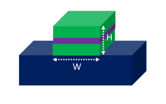
In this work, we propose and demonstrate a symmetric stack where a central high index material is sandwiched between two medium index materials. The high index material is chosen as amorphous silicon (a-Si), and the medium index material is chosen as silicon nitride (). Both and can be deposited by standard deposition techniques, and they are promising materials for PIC [8, 9, 10]. Figure 1(a) and 1(b) shows a schematic and the geometrical parameters in cross-sectional view of the proposed structure, respectively. The structure has three geometrical parameters that can be varied to tune the properties of the waveguide. Height (’H’) and width (’W’) are similar parameters as in the wire waveguide. But, this structure has an additional parameter, the relative thickness of high index material with respect to the total height. This makes the waveguide properties highly tunable. The relative thickness of high-index material and medium-index material can be replaced by a single variable, simplifying the analysis. The relative thickness of high index material will be referred to as fraction (‘f’) from here on. The parameter fraction is defined as f = Thickness of high index/Total height (’H’). The parameter ‘f’ provides a powerful way to analyze the system by having a single variable instead of two thickness variables. The implications of the fraction on the waveguide properties are discussed in detail for both air and oxide clad, followed by a demonstration of and gratings for fiber-to-chip coupling in the proposed structure. The measured coupling efficiency for grating is -3.27 dB per coupler, and grating is -8 dB per coupler. Finally, the excitation of a particular mode (TE/TM) is confirmed by thermo-optic measurements based on the spectral response of a ring resonator.
2 Waveguide Design
A wire waveguide can be designed by appropriately choosing the width and height to suit a particular application. The proposed waveguide can be further tuned by varying the fraction. This unique parameter provides flexibility in effective index tuning, confinement in different materials and polarization birefringence control which are restricted in uniform index waveguides. We consider waveguide design with top cladding as air and oxide. The height of the proposed waveguide is fixed at 500 nm to ensure mode confinement in the entire work.
2.1 Waveguide design in air clad
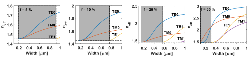
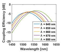
The waveguide design is performed using a numerical mode-solver. The refractive index of SiN is considered as 1.89 and a-Si as 3.54 and the wavelength of operation is 1550 nm. Simulations were performed to study the effect of fraction (f) on the waveguide properties. The evolution of effective mode index as a function of width is found for various f, and a few of them are shown in Figure 2. In fig.2, the single-mode region is marked by the shaded area. For higher fraction f, we observe propagating with higher index than the mode in the single-mode regime.
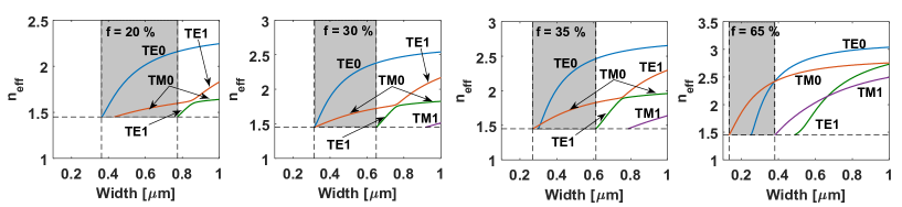
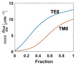
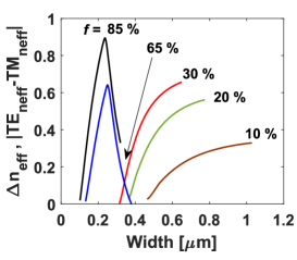
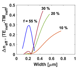
The effective index is a fundamental property that determines the functional property of various waveguide devices. Variation in the effective index due to width and fraction will result in suboptimal device performance. Figure 3(a) shows the at different fractions f in the single-mode regime. It can be clearly observed that the mode is highly sensitive to width variation and f variation than the mode. This implies that the modes are tolerant to layer-thickness and width variation compared to .
It is important to note that confinement of light is in both and due to the hybrid structure of the waveguide. The waveguide will be henceforth referred to as hybrid waveguide. The hybrid nature of the waveguide demands calculation of confinement for both and regions. The confinement factor in a region R is defined as [11]:
| (1) |
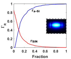
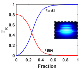
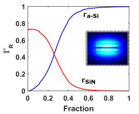
The confinement in the waveguide depends on the polarization. Figure 3(b) and 3(c) show the confinement in the and layer for a 700 nm wide waveguide to have a broad range of fraction values where the width lies in the single mode region. It can be clearly observed that for mode the light confinement is higher in the layer for f 10 % and for mode it is higher for f 25 %. Thus, the factor f can be tuned to have desired confinement in either material to best suit any application. An interesting observation is that the confinement of light for a given geometry in and layers is polarization-dependent. Light can be confined into a higher index with mode and into a medium index with mode. It can be concluded from Figures 3(b) and 3(c) that a fraction of 20 % is ideal for confining light into with mode and into with mode. This typical behaviour can be explained by the boundary conditions of Maxwell’s equation. The normal component of displacement density should be continuous, making the electric field in the layer for mode as
| (2) |
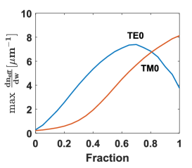
In some applications, such as wavelength division multiplexing (WDM) a low polarization sensitivity [12] is desired. However, in some cases, high polarization extinction can be used for creating polarization-selective phase delay[13]. Thus, a flexible control of birefringence () is highly desirable. In the hybrid platform, birefringence can be controlled by adjusting ‘f’. Figure 3(d) shows the birefringence for various fractions in the single mode region. The slope of birefringence vs width continues to increase with fraction. Thus, the trend seems to push the birefringence to higher values. But, it is observed that between f = 35 % to f = 65% , there exists an inflection point where the birefringence becomes negligible. This can be exploited to suit the particular application.
2.2 Waveguide design in oxide clad
The simulations of sandwich waveguide with oxide clad are performed to study the impact of fraction f on the waveguide properties. The reduction in the refractive index contrast shifts the single-mode regime towards lower waveguide widths (Fig. 4). For air clad, it is observed that there is anti-crossing between modes of different order indicating the existence of a hybrid mode that can result in undesirable mode conversions. Since the index-contrast is reduced, the is lowered, which implies that the waveguides are tolerant to dimensional variations, unlike air-clad.
The confinement factor is calculated with the same procedure as for air clad. Figures 5(b) and 5(c) show confinement factor for and mode with oxide clad. The width is fixed at 500 nm. The trend is very similar to air clad. In both air-clad and oxide clad, a 20 % fraction is suitable for light confinement. Figure 5(d) shows the birefringence for oxide clad. The sensitivity to polarization for oxide clad is less than air clad. For larger values of fraction, the peak is flatter compared to air clad, giving a width tolerant birefringence.
3 Fiber-chip coupling
3.1 Design and fabrication of and surface grating couplers
Surface grating fiber-chip couplers are a versatile fiber-chip coupling scheme [14]. A grating fiber-chip coupler for and is designed and developed to demonstrate the proposed waveguide in the 1550 nm wavelength band. The height in all the designs is considered as 500 nm and f as 20 %. The resulting thickness for the top and bottom layers is 200 nm, and is 100 nm. For efficient coupling into mode, the layer is etched, and for mode entire stack is etched to pattern the gratings. The designs are aimed at optimum diffraction to facilitate coupling into a given mode. The coupling efficiency (CE) is optimized by varying period, angle, duty-cycle, etch depth (only for mode) and bottom oxide thickness by performing 2D finite difference time domain (FDTD) simulations. Particle swarm optimization (PSO) is used to optimize the coupling efficiency instead of parametric sweep due to a large number of parameters[15]. The dependence of various parameters is discussed in detail in the results section. The simulation results are summarized in table 1.
| Parameter [units] | ||
|---|---|---|
| 1.94 | 1.58 | |
| Etched layer for grating | layer | Full etch |
| Coupling Efficiency [dB] | -2.52 | -3.9 |
| 1 dB bandwidth [nm] | 57.6 | 54.4 |
| 3 dB bandwidth [nm] | 98 | 94 |
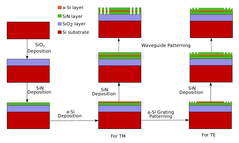
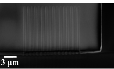
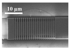
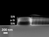
The grating designs are fabricated in the desired layer stack. The stack is prepared by depositing , and using plasma-enhanced chemical vapour depositing process. The grating and waveguide patterning is done using the electron-beam lithography process. Figure 6 shows the process flow for fabrication of both and gratings and the waveguide. The entire stack is deposited for mode, followed by lithography and pattern transfer of both gratings and waveguide through etching. In mode, the gratings are patterned in the layer, followed by deposition. After that, the waveguide is patterned on the completed stack. Figures 7(a) and 7(b) show the top view of the and gratings respectively. Figure 7(c) shows the cross-section of a 700 nm wide waveguide with three layers.
The TE and TM gratings were made in different runs with a common oxide layer. The deposited oxide thickness is 1570 nm. The deposited thickness of SiN layer is 220 nm for TE gratings and 214 nm for TM gratings. The deposited thickness of a-Si layer is 98 nm for TE gratings and 115 nm for TM gratings. The etching of SiN layers was done with and and a-Si was done with and .
The grating test structures are made on a 12 m wide waveguide with number of periods. The fabricated devices are characterised using a superluminescent diode (SLED) as a source and a spectrum analyzer. The input polarisation is controlled by polarization paddles. The coupling efficiency is calculated by normalizing the transmission to the source spectrum.
3.2 Results and analysis
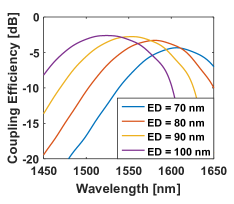
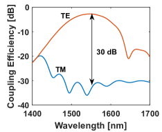
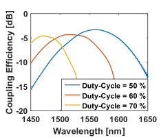
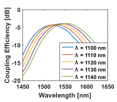
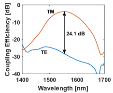
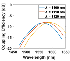
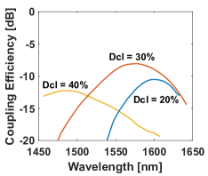
Figure 8 depicts the summary of simulation and measured spectral response of grating coupler. Figures 8(a), 8(b) and 8(c) show the effect of etch depth (ED), period and duty-cycle, respectively, on the coupling efficiency of a grating coupler. It is known that the 1D gratings are polarization sensitive, Fig. 8(d) depicts the simulated extinction between and input on gratings. The experimental validation is depicted in Figures 8(e) and 8(f) showing the measured spectral response of gratings with varying period and duty-cycle. The Bragg’s law can be used to verify the coupler characteristics. The grating period is related to the coupling wavelength (), fibre angle () and effective index () as,
| (3) |
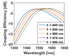
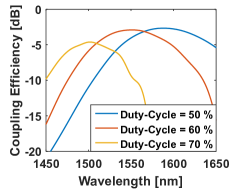
We observe that there is a red shift of the spectrum with an increase in period, both in simulation and experiment. This can be explained from Eq. (3), where the centre wavelength is directly proportional to period. With an increase in duty-cycle, the spectrum is blue shifted for both simulation and experimental measurements and can be verified from Eq. (3). The increase in duty-cycle decreases the effective index resulting in blue shift. The etch depth increase also results in blue shift due to decrease in effective index. The extinction for polarized light is about 30 dB with respect to polarized light in mode gratings.
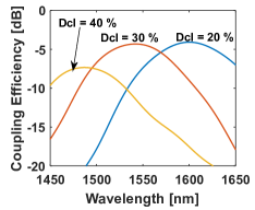
Similar analysis is done for mode gratings. Figures 9(a) and 9(b) show the simulated variation of spectral response of gratings with period and duty-cycle. Figure 9(c) shows the simulated extinction between and input on gratings. Figures 9(d) and 9(e) show the measured variation of spectral response of gratings with period and duty-cycle.
| Data | CE [dB] | [nm] | 1 dB BW [nm] | 3 dB BW [nm] | CE [dB] | [nm] | 1 dB BW [nm] | 3 dB BW [nm] |
|---|---|---|---|---|---|---|---|---|
| Optimum design | -2.52 | 1547 | 57.6 | 98 | -3.9 | 1553 | 54.4 | 94 |
| Fabricated/ Measured | -3.27 | 1561 | 56.8 | 100 | -8 | 1572 | 51 | 92 |
| Fabricated device simulation | -3.06 | 1560 | 70 | 127 | -8.16 | 1570 | 50 | 113 |
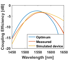
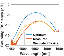
The best measured coupling efficiency for gratings is -3.27 dB/coupler and for gratings is -8 dB per coupler. Figure 10(a) and 10(b) show the comparative spectral response of the optimally designed, fabricated device and measured device for and mode, respectively. Table 2 summarizes measurement and simulation grating performance.
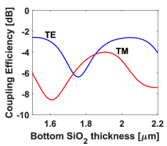
The grating coupler efficiency is close to the optimum design. However, a red shift in the spectral response from the optimized value is due to a slightly lower than desired etch depth. The coupling efficiency for mode is 4 dB less than optimum. This can be attributed to the SiO2 thickness variation as shown in Figure 9(f) [16]. The energy coupling efficiency can be further increased by employing a bottom Bragg reflector[17].
4 Confirmation of and mode
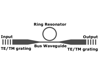
4.1 Ring Resonator in the hybrid platform
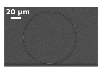
The propagation of the desired mode in the waveguide can be characterized by using a wavelength selective device, such as a ring resonator. The spectral characteristics of a ring resonator depend on the group index of resonant mode in the cavity. By calculating the group index from the free-spectral range (FSR), one could identify the cavity mode polarization [18]. The above-mentioned stack is used to fabricate a 100 m diameter ring resonator. The waveguide width is kept at 700 nm to accommodate both and (Fig. 2). A gap of 250 nm and 350 nm is used between the bus and the ring for and rings. Figure 11(a) shows the schematic and SEM image of a device. Waveguide tapers of length 250 m are used to connect the 700 nm single-mode waveguide to the grating fiber-couplers made on 12 m width waveguide. The in and out couplers are designed to be either or to selectively excite single polarization in the waveguide.
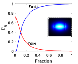
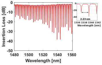
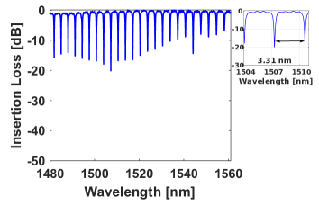
Figures 12(a) and 12(b) show the normalized spectral response of the and ring, respectively. An FSR of 2.23 nm and 3.31 nm is measured for and resonators. The corresponding calculated group index is 3.38 and 2.18 against an expected 3.48 and 2.33 for and , respectively. This shows an excellent agreement and confirmation of corresponding polarization excitation by the grating couplers. In addition, we observe a quality factor of 3400 for the ring and 4000 for the ring. The resonance shows a better quality factor due to lower scattering from the etched sidewalls. The loss is primarily due to the interface between the sandwich layers. This is further confirmed by a lower insertion loss of about -1 dB from the ring compared to -2.2 dB from a ring resonator.
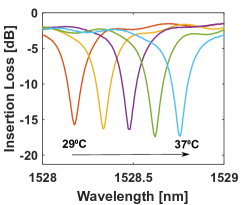
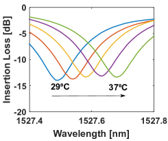
4.2 Thermal response and mode confinement.
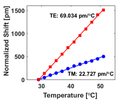
Unlike a solid single material core, the mode distribution in the hybrid waveguide is specific to polarization and . As discussed in section 2, The mode is primarily confined in the while the is distributed between the two layers. Since the mode confinement is hybrid, the confinement can be confirmed using the thermo-optic response of the two modes [19, 20, 21]. The thermo-optic response of the above-mentioned rings is characterized by heating the substrate using a Peltier element and a temperature controller. The temperature is tuned from 29 ∘C to 51 ∘C in steps of 2 ∘C. Figures 13(a) and 13(b) show the shift in resonance wavelength with temperature. The resonance shift is 69 pm/∘C for the ring and 23 pm/∘C for the ring, as shown in Figure 13(c). The confirmation of the excited mode and confinement is done by deriving the thermo-optic coefficient (TOC) of the individual materials.
The effective TOC is found from the spectral shift (d/dT ) as given by [19].
| (4) |
The effective TOC of the sandwich waveguide is the superposition of TOC of individual layers and the electric field confinement () in the particular layer for a given mode by [20].
| (5) |
The electric field confinement () in the ith layer is calculated by taking the electric field distribution [22].
| (6) |
Equation 5 is solved simultaneously for and polarizations to find TOC of and . The calculations are summarized in table 3. The TOC for is found to be and for which are close to the values found in literature [23, 24] confirming the analysis.
| Parameter [units] | mode | mode |
|---|---|---|
| Measured | 69.034 | 22.727 |
| 0.685 | 0.076 | |
| 0.46 | 0.718 | |
| 3.38 | 2.18 |
5 Conclusion
We have demonstrated a hybrid waveguide platform with a high-index material sandwiched between two medium-index materials. The proposed waveguide configuration offers a versatile platform to tune the effective index, confinement and polarization behaviour. We have demonstrated grating fiber-chip couplers for coupling into both and modes with a coupling efficiency of -3.27 dB and -8 dB per coupler with a 3dB bandwidth of 100 nm. Using thermo-optic response, we confirm the polarisation-dependent mode confinement in high and medium-index layers in the waveguide. We believe the proposed waveguide configuration would help to realize interesting functionalities that are limited by the single material solid-core waveguide platforms.
6 Acknowledgement
We thank DST-SERB for funding this research. We also acknowledge funding from MHRD, MeitY and DST for supporting facilities at the Centre for Nanoscience and Engineering (CeNSE), Indian Institute of Science, Bangalore.
References
- [1] W. Bogaerts, S. K. Selvaraja, Compact single-mode silicon hybrid rib/strip waveguide with adiabatic bends, IEEE Photonics Journal 3 (3) (2011) 422–432. doi:10.1109/JPHOT.2011.2142931.
- [2] V. R. Almeida, Q. Xu, C. A. Barrios, M. Lipson, Guiding and confining light in void nanostructure, Optics Letters (2004). doi:10.1364/ol.29.001209.
-
[3]
M. Brun, P. Labeye, G. Grand, J.-M. Hartmann, F. Boulila, M. Carras,
S. Nicoletti,
Low
loss SiGe graded index waveguides for mid-IR applications, Optics Express
22 (1) (2014) 508.
doi:10.1364/OE.22.000508.
URL https://www.osapublishing.org/oe/abstract.cfm?uri=oe-22-1-508 - [4] M. Z. Alam, X. Sun, M. Mojahedi, J. S. Aitchison, Augmented low index waveguide for confining light in low index media, Laser and Photonics Reviews (2017). doi:10.1002/lpor.201500224.
- [5] D. Dai, Y. Tang, J. E. Bowers, Mode conversion in tapered submicron silicon ridge optical waveguides, Optics Express (2012). doi:10.1364/OE.20.013425.
- [6] D. Vermeulen, K. Van Acoleyen, S. Ghosh, S. Selvaraja, W. A. D. De Cort, N. A. Yebo, E. Hallynck, K. De Vos, P. P. P. Debackere, P. Dumon, W. Bogaerts, G. Roelkens, D. Van Thourhout, R. Baets, Efficient tapering to the fundamental quasi-TM mode in asymmetrical waveguides, European Conference on Integrated Optics (2010).
- [7] C. G. H. Roeloffzen, M. Hoekman, E. J. Klein, L. S. Wevers, R. B. Timens, D. Marchenko, D. Geskus, R. Dekker, A. Alippi, R. Grootjans, A. van Rees, R. M. Oldenbeuving, J. P. Epping, R. G. Heideman, K. Wörhoff, A. Leinse, D. Geuzebroek, E. Schreuder, P. W. L. van Dijk, I. Visscher, C. Taddei, Y. Fan, C. Taballione, Y. Liu, D. Marpaung, L. Zhuang, M. Benelajla, K.-J. Boller, Low-loss si3n4 triplex optical waveguides: Technology and applications overview, IEEE Journal of Selected Topics in Quantum Electronics 24 (4) (2018) 1–21. doi:10.1109/JSTQE.2018.2793945.
-
[8]
S. Kumar Selvaraja, M. Schaekers, W. Bogaerts, D. Van Thourhout,
Deposited
amorphous silicon-on-insulator technology for nano-photonic integrated
circuits, Optics Communications 313 (2014) 210–216.
doi:10.1016/j.optcom.2013.10.033.
URL http://dx.doi.org/10.1016/j.optcom.2013.10.033https://linkinghub.elsevier.com/retrieve/pii/S0030401813009504 -
[9]
S. K. Selvaraja, E. Sleeckx, M. Schaekers, W. Bogaerts, D. V. Thourhout,
P. Dumon, R. Baets, Low-loss
amorphous silicon-on-insulator technology for photonic integrated
circuitry, Optics Communications 282 (9) (2009) 1767–1770.
doi:10.1016/j.optcom.2009.01.021.
URL http://dx.doi.org/10.1016/j.optcom.2009.01.021https://linkinghub.elsevier.com/retrieve/pii/S0030401809000418 -
[10]
R. Baets, A. Z. Subramanian, S. Clemmen, B. Kuyken, P. Bienstman, N. Le
Thomas, G. Roelkens, D. Van Thourhout, P. Helin, S. Severi,
Silicon
Photonics: silicon nitride versus silicon-on-insulator, in: Optical Fiber
Communication Conference, OSA, Washington, D.C., 2016, p. Th3J.1.
doi:10.1364/OFC.2016.Th3J.1.
URL https://www.osapublishing.org/abstract.cfm?URI=OFC-2016-Th3J.1 -
[11]
M.-C. Tien, J. F. Bauters, M. J. R. Heck, D. J. Blumenthal, J. E. Bowers,
Ultra-low
loss Si_3N_4 waveguides with low nonlinearity and high power handling
capability, Optics Express 18 (23) (2010) 23562.
doi:10.1364/OE.18.023562.
URL https://www.osapublishing.org/oe/abstract.cfm?uri=oe-18-23-23562 -
[12]
P. Trinh, S. Yegnanarayanan, F. Coppinger, B. Jalali,
Silicon-on-insulator
(SOI) phased-array wavelength multi/demultiplexer with extremely
low-polarization sensitivity, IEEE Photonics Technology Letters 9 (7)
(1997) 940–942.
doi:10.1109/68.593358.
URL http://ieeexplore.ieee.org/document/593358/ -
[13]
S.-H. Yang, M. L. Cooper, P. R. Bandaru, S. Mookherjea,
Giant
birefringence in multi-slotted silicon nanophotonic waveguides, Optics
Express 16 (11) (2008) 8306.
doi:10.1364/OE.16.008306.
URL https://www.osapublishing.org/oe/abstract.cfm?uri=oe-16-11-8306 - [14] S. Nambiar, P. Sethi, S. K. Selvaraja, Grating-assisted fiber to chip coupling for SOI photonic circuits, Applied Sciences (Switzerland) 8 (7) (2018) 1–22. doi:10.3390/app8071142.
- [15] J. Kennedy, R. Eberhart, Particle swarm optimization, in: Proceedings of ICNN’95 - International Conference on Neural Networks, Vol. 4, 1995, pp. 1942–1948 vol.4.
-
[16]
V. A. Sychugov,
Optimization
and control of grating coupling to or from a silicon-based optical
waveguide, Optical Engineering 35 (11) (1996) 3092.
doi:10.1117/1.601048.
URL http://opticalengineering.spiedigitallibrary.org/article.aspx?doi=10.1117/1.601048 -
[17]
S. K. Selvaraja, D. Vermeulen, M. Schaekers, E. Sleeckx, W. Bogaerts,
G. Roelkens, P. Dumon, D. Van Thourhout, R. Baets,
Highly
efficient grating coupler between optical fiber and silicon photonic
circuit, in: Conference on Lasers and Electro-Optics/International Quantum
Electronics Conference, OSA, Washington, D.C., 2009, p. CTuC6.
doi:10.1364/CLEO.2009.CTuC6.
URL https://www.osapublishing.org/abstract.cfm?URI=CLEO-2009-CTuC6 - [18] W. Bogaerts, P. de Heyn, T. van Vaerenbergh, K. de Vos, S. Kumar Selvaraja, T. Claes, P. Dumon, P. Bienstman, D. van Thourhout, R. Baets, Silicon microring resonators, Laser and Photonics Reviews 6 (1) (2012) 47–73. doi:10.1002/lpor.201100017.
-
[19]
J. Teng, P. Dumon, W. Bogaerts, H. Zhang, X. Jian, X. Han, M. Zhao,
G. Morthier, R. Baets,
Athermal
Silicon-on-insulator ring resonators by overlaying a polymer cladding on
narrowed waveguides, Optics Express 17 (17) (2009) 14627.
doi:10.1364/OE.17.014627.
URL https://www.osapublishing.org/oe/abstract.cfm?uri=oe-17-17-14627 - [20] S. Feng, K. Shang, J. T. Bovington, R. Wu, B. Guan, K.-T. Cheng, J. E. Bowers, S. J. Ben Yoo, Athermal silicon ring resonators clad with titanium dioxide for 13µm wavelength operation, Optics Express 23 (20) (2015) 25653. doi:10.1364/oe.23.025653.
-
[21]
V. Mere, R. Kallega, S. K. Selvaraja,
Efficient
and tunable strip-to-slot fundamental mode coupling, Optics Express 26 (1)
(2018) 438.
doi:10.1364/oe.26.000438.
URL https://www.osapublishing.org/abstract.cfm?URI=oe-26-1-438 -
[22]
T. Visser, B. Demeulenaere, J. Haes, D. Lenstra, R. Baets, H. Blok,
Confinement and modal
gain in dielectric waveguides, Journal of Lightwave Technology 14 (5)
(1996) 885–887.
doi:10.1109/50.495172.
URL http://ieeexplore.ieee.org/document/495172/ -
[23]
F. G. Della Corte, M. E. Montefusco, L. Moretti, I. Rendina, A. Rubino,
Study of the
thermo-optic effect in hydrogenated amorphous silicon and hydrogenated
amorphous silicon carbide between 300 and 500 K at 1.55 m, Applied
Physics Letters 79 (2) (2001) 168–170.
doi:10.1063/1.1383056.
URL http://aip.scitation.org/doi/10.1063/1.1383056 -
[24]
A. W. Elshaari, I. E. Zadeh, K. D. Jons, V. Zwiller,
Thermo-Optic
Characterization of Silicon Nitride Resonators for Cryogenic Photonic
Circuits, IEEE Photonics Journal 8 (3) (2016) 1–9.
doi:10.1109/JPHOT.2016.2561622.
URL http://ieeexplore.ieee.org/document/7463458/