A planar defect spin sensor in a two-dimensional material susceptible to strain and electric fields
Abstract
The boron-vacancy spin defect () in hexagonal boron nitride (hBN) has a great potential as a quantum sensor in a two-dimensional material that can directly probe various external perturbations in atomic-scale proximity to the quantum sensing layer. Here, we apply first principles calculations to determine the coupling of the electronic spin to strain and electric fields. Our work unravels the interplay between local piezoelectric and elastic effects contributing to the final response to the electric fields. The theoretical predictions are then used to analyse optically detected magnetic resonance (ODMR) spectra recorded on hBN crystals containing different densities of centres. We prove that the orthorhombic zero-field splitting parameter results from local electric fields produced by surrounding charge defects. By providing calculations of the spin-strain and spin-electric field couplings, this work paves the way towards applications of centres for quantitative electric field imaging and quantum sensing under pressure.
I Introduction
Electric and strain field effects are highly important ingredients in the tight control of solid-state spin defects for quantum technology applications. The accurate knowledge of the couplings to these perturbations can be harnessed either actively, e.g. for tuning the magneto-optical properties of the defect, or passively, e.g. for sensing its close environment. Particular attention is currently given to spin defects embedded in two-dimensional (2D) van der Waals materials Toth and Aharonovich (2019); Chakraborty et al. (2019); Ye et al. (2019); Vaidya et al. (2023). The main advantage of a 2D host is the proximity of the quantum defect to the surface, which improves both its optical efficiency Li et al. (2019) and sensing capabilities Vaidya et al. (2023). One of these 2D materials is hexagonal boron nitride (hBN), which can be exfoliated down to the mono-layer limit without compromising its chemical stability Song et al. (2010); Park et al. (2014). Owing to its large optical band gap ( Cassabois et al. (2016)), hBN hosts optically-active point defects in a wide range of wavelengths. Once isolated at the individual scale, defects in hBN were first studied as single photon emitters, providing narrow and tunable emission lines, high brightness, and perfect photostability Tran et al. (2016); Martínez et al. (2016); Vogl et al. (2018); Li et al. (2022); Jungwirth et al. (2016); Grosso et al. (2017); Noh et al. (2018); Mendelson et al. (2020); Sajid et al. (2020a). In addition, it was recently shown that the electron spin resonance frequencies of some defects can be inferred through optically detected magnetic resonance (ODMR) methods, providing a central resource for quantum sensing applications Chejanovsky et al. (2021); Stern et al. (2022); Sajid et al. (2018); Weston et al. (2018); Sajid et al. (2020b); Auburger and Gali (2021); Gottscholl et al. (2020).
To date, the negatively-charged boron-vacancy centre () is the only point defect in hBN possessing an ODMR response whose microscopic structure has been unambiguously identified Gottscholl et al. (2020); Abdi et al. (2018); Ivády et al. (2020); Haykal et al. (2022). This defect, which can be readily created by irradiation, ion-implantation and laser writing techniques Li et al. (2021); Murzakhanov et al. (2021); Kianinia et al. (2020); Guo et al. (2022); Gao et al. (2021a), has been recently employed for sensing magnetic fields Gottscholl et al. (2021); Gao et al. (2021b); Huang et al. (2022); Kumar et al. (2022); Healey et al. (2023), strain Yang et al. (2022); Lyu et al. (2022), and temperature Gottscholl et al. (2021); Liu et al. (2021); Healey et al. (2023). In this context, the purpose of the present work is to provide an accurate description of the coupling of centres in hBN to strain and electric fields.
Under optical illumination, the centre exhibits a very broad emission in the near-infrared Gottscholl et al. (2020). Although an experimental work has reported a zero-phonon-line (ZPL) at Qian et al. (2022), a recent theoretical study has claimed that the full emission is phonon-assisted since optical transitions between electronic states are forbidden Libbi et al. (2022). As a consequence, the optical emission is intrinsically dim and only dense ensembles of centres could be detected in experiments so far. Theory further identified that the centre has a spin triplet ground state () with symmetry Ivády et al. (2020). In the absence of external perturbations, the ground state spin Hamiltonian only involves spin-spin interaction and reads as
| (1) |
The axial zero-field-splitting (ZFS) parameter separates the and spin sublevels, the notation referring to the spin projection along the -axis () of the hBN crystal. Interestingly, ODMR spectra recorded on ensembles of centres usually indicate two magnetic resonances at frequencies , with GHz and MHz Gottscholl et al. (2020). These measurements thus reveal an additional orthorhombic splitting () of the levels, which is in contradiction with the symmetry of the centre. While this splitting was originally attributed to strain effects in the hBN crystal leading to a reduced symmetry of the defect Gottscholl et al. (2020); Guo et al. (2022), a recent study suggested that it results instead from the interaction with a local electric field Gong et al. (2022). However, no microscopic picture has been applied to interpret these results. More generally, there is an urgent need to understand the coupling of strain and electric fields to defect spins, which is an exemplary quantum sensor in a van der Waals material.
In this paper, we employ first principles simulations to determine the effect of external electric and strain fields on the ground state electronic spin structure of centres in hBN. We show that in most of the experimental conditions the defect experiences fluctuating electric fields that leads to an orthorhombic splitting in ODMR spectra recorded at zero external magnetic field. We identify the microscopic origin of this effect and determine the spin-strain and spin-electric field coupling parameters. We then compare these results to experimental ODMR spectra recorded from neutron-irradiated hBN crystals containing different densities of centres. Our study proves that the orthorhombic ZFS is caused by fluctuating electric fields and suggest that the coupling strengths of the centres to strain and electric fields are comparable to those of the nitrogen-vacancy (NV-) centre in diamond Barson et al. (2017); Van Oort and Glasbeek (1990).
II Results
II.1 Defect structure and spin-spin interaction
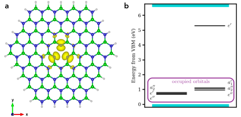
The centre in hBN is a single vacancy at the boron site in the negatively charged state possessing point symmetry (Fig. 1a). In the following, the spin properties of the centre are calculated using a large hydrogen-terminated mono-layer flake model (see Methods). The coordinate frame is defined as span the plane of the hBN layer, with and along the zigzag and armchair directions of the hexagonal lattice, respectively. The Kohn-Sham levels in the spin-polarised calculations are plotted in Fig. 1b, showing nearby double degenerate and levels and non-degenerate and levels leaving two holes in the orbital of the spin minority spin channel. This constitutes the spin triplet ground state of the centre, in agreement with previous calculations Abdi et al. (2018); Ivády et al. (2020); Sajid et al. (2020c). Importantly, the spin density is dominantly localised in-plane on the three dangling bonds of the neighbouring nitrogen atoms (Fig. 1a), as recently confirmed experimentally by pulsed electron-nuclear double resonance techniques Gracheva et al. (2023).
Starting with an unperturbed symmetry, the mono-layer flake model leads to an axial ZFS parameter [see Eq. (1)], a value in fair agreement with the experimental results . In the Supplementary Note 1, we show that the mono-layer flake model well represents the bulk environment around the defect because the spin density is fully localised into the hBN plane. Although there is about 6% discrepancy in the absolute value of the parameters obtained from our theoretical approach and the experimental data, the accuracy in the variation of the zero-field-splitting parameters upon external perturbations can be reliably obtained thanks to the cancellation of numerical errors in partial derivatives.
In the next sections, we compute the coupling coefficients of the centre to strain and electric fields. We assume that the strengths of theses fields are much smaller than the Coulomb interaction between the electrons, so that strain and electric fields can be considered as perturbations. We analyse how these interactions can lead to an orthorhombic ZFS parameter, that splits the levels upon axial symmetry breaking.
II.2 Strain field interaction
We start the analysis of external perturbations with the strain field case. We construct the interaction Hamiltonian analogously to previous calculations performed on the centre in diamond featuring symmetry Udvarhelyi et al. (2018). In the linear approximation, the bi-linear forms of the second rank tensor of the external strain are connected to the bi-linear forms of the second rank tensor by scalar coupling coefficients . We write the interaction in a symmetry-adapted form to retain only the linearly independent couplings, i.e. we construct the irreducible representation basis in symmetry from the components of the strain and spin tensors. These transform as quadratic spatial coordinates, e.g. and both belong to the totally symmetric irreducible representation. The interaction Hamiltonian is totally symmetric, thus only the products of the same irreducible representations of the strain and spin are valid combinations.
According to the theory of invariants, the Hamiltonian describing the interaction of the centre with strain can be formulated as
| (2) |
where are the coupling coefficients between bi-linear forms of the strain matrix elements and bi-linear forms of the spin projection operators reflecting a symmetry-adapted form of . Note that the out-of-plane strain components are not included in the Hamiltonian because we consider a single-layer flake model. However, these couplings are expected to be minor for a bulk model as well since out-of-plane () distortions have a small impact on the in-plane hBN structure that contains the spin density of the centre (see Supplementary Note 2).
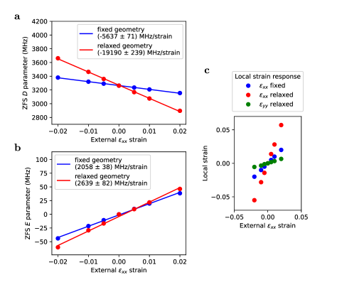
To calculate the coupling coefficients , we specify uniform strain of a single element in the strain tensor in each calculation and apply it to our model (see Methods). We do so for each symmetrically non-equivalent components in Eq. (II.2), i.e. for and . We then calculate the resulting axial and orthorhombic ZFS parameters (see red data in Fig. 2a,b) and obtain the coupling coefficients as the partial derivatives
| (3) | ||||
| (4) | ||||
| (5) | ||||
| (6) | ||||
| (7) |
where are components of the ZFS -matrix defined by alternate form of the interaction . The negative sign of implies a larger (smaller) axial ZFS parameter for compressive (tensile) external strain, in line with the decrease (increase) of the distance between the localised spin density lobes.
We now analyse how the microscopic structure of the defect affects the response to the strain. To this end, we carried out calculations for which we strained the lattice of the defective model without allowing any local ionic relaxation around the defect and then calculated the change in the ZFS parameters (blue points in Fig. 2a,b). After allowing local relaxation under the externally applied strain (red points in Fig. 2a,b), we can define the local geometry changes in the close vicinity of the defect. The local strain is defined from the deformation of the triangle spanned by the three neighbouring nitrogen atom positions. We plot this local strain as a function of the external strain in Fig. 2c. We identify a large increase in the same component () of the local strain after relaxation. Moreover, an additional component is also activated. We attribute this effect to the smaller local stiffness at the vacancy site originating from the broken bonds. During the relaxation of the defect under external strain, it is energetically favourable for the vacancy site to accommodate an increased strain compared to the externally applied one, thus lowering the strain enthalpy of the host material in its vicinity. Generally, the same strain enhancement is expected in defects with dangling or weaker bonds than the ones in its host material, making this type of qubits more sensitive strain sensors. The increased local strain after relaxation reflects in the increase of the ZFS strain coupling strength as well. Note that relaxation under external sheer strain () shows similar trend in the ZFS coupling strength.
Finally, we convert the strain-spin coupling strengths to stress couplings, as stress is usually more accessible and controllable in experiments than strain. Based on the experimentally available elastic parameters of and in bulk hBN Bosak et al. (2006), we calculate the stress coupling coefficients as
| (8) | ||||
| (9) |
where elements are the second order elastic constants (stiffness tensor) in the Voigt notation. The relation between the strain () and stress () can be then formulated in linear elasticity as
| (10) |
With the above conversion, the Hamiltonian takes a similar form to Eq. (II.2) using the stress coupling coefficients
| (11) | ||||
| (12) |
Importantly, our calculations already indicate that , such that spin-stress coupling mostly leads to variations of the axial ZFS parameter without inducing a significant orthorhombic splitting.
II.3 Electric field interaction
The Hamiltonian of the electric field coupling is constructed analogously to the strain coupling as
| (13) |
where is the coupling coefficient between linear forms of the electric field vector and bi-linear forms of the spin projection operators reflecting a symmetry-adapted form of . We note that the parallel component of the electric field () with respect to the hBN plane normal vector belongs to the irreducible representation, and it cannot couple to either or representations of the spin operators. As a result, the interaction with an electric field only introduces an orthorhombic splitting without inducing variations of the axial ZFS parameter .
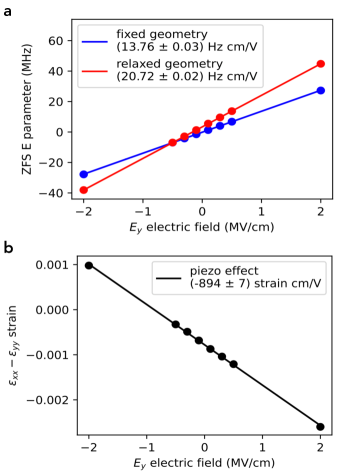
We apply homogeneous electric field to the defective hBN model. The coupling coefficient can be calculated as the partial derivative of the ZFS parameter (see Fig. 3a)
| (14) |
We note that a recent experimental work has estimated the coupling strength of the parameter to the electric field as Gong et al. (2022), which is in the same order of magnitude as our first-principle results.
We now analyse the geometry relaxation under the applied external electric field similarly as for the case of the strain perturbation discussed above. We can identify an accompanying piezo effect resulting in and additional strains for the applied and electric fields, respectively. The former calculation is shown in Fig. 3b. This effect enhances the coupling strength to the electric field by a factor of (compare blue and red points in Fig. 3a).
The microscopic origin of the piezo enhancement effect can be explained by changes in electrostatic interactions in the vicinity of the defect under the applied external electric field. We obtain a significant change in the partial charge distribution of the strongly polarised bonds around the vacancy defect depending on the relative direction of the external electric field. This implies a redistribution of the electron density by the electric fields, which generates quantum mechanical forces on the ions. The origin of this effect can be detailed in the example of the vacancy-neighbour nitrogen atom in the direction and its boron neighbours. Without the external electric field applied, the B-N bonds are polarised with an effective dipole moment pointing from N to B. The applied field in the positive (resp. negative) direction increases (resp. decreases) the original charge separation and the effective dipole moment. This results in an additional effective attractive (resp. repulsive) force along the B-N bond and an outward (resp. inward) relaxation of the nitrogen atom relative to the vacancy site. We identify this additional relaxation as the piezo response. Thus, the relaxation of the nitrogen atom is in the same direction as the electric field. This finally enhances the symmetry-breaking effect of the electric field and consequently its coupling to the parameter.
II.4 ODMR simulation
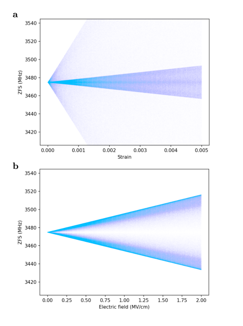
In the experimental ODMR signal of the centre, a small orthorhombic splitting was reported despite its contradiction with the defect symmetry. Recently, the effect was attributed to the local electric field originating from nearby charged defects without providing arguments from microscopic picture of the defect Gong et al. (2022). Firstly, we simulate the ZFS parameters of a single defects affected by the presence of uniformly distributed random local strain or electric fields of given magnitudes. We sample 1000 random configurations for each given magnitude and visualise the corresponding eigenvalues of the ZFS Hamiltonian as a scatter plot as a function of the perturbation magnitude. From the simulations shown in Fig. 4, we conclude that the splitting can be exclusively attributed to the local electric field, while the effect of strain leads to a broadening of the signal. The sharp splitting originates from the large difference in the magnitudes of the couplings of the and parameters to the external fields. We can describe this with the ratio of the coupling strengths. In the case of the electric field, the parameter coupling is symmetry forbidden, , leading to a sharp splitting of the magnetic resonances. In the case of the strain field, we calculate , which leads to a dominating shift in the ODMR signal with broadening of the integrated spectrum. We note that a similar effect was already observed and simulated for the centre in diamond Mittiga et al. (2018).
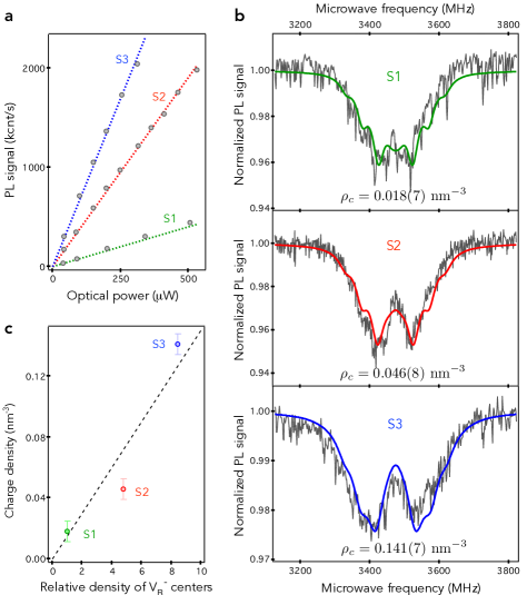
We now use our theoretical predictions to analyse experimental ODMR spectra recorded at zero external magnetic field. To this end, we rely on three hBN crystals (S1, S2 and S3) with different densities of V centres created by neutron irradiation. Their optical properties are analysed with a confocal microscope operating at room temperature under green laser illumination (see Methods). All crystals exhibit the characteristic emission spectrum of V centres with a broad spectral line in the near infrared. The relative density of V centres is estimated by recording the evolution of the PL signal with the optical excitation power [Fig. 5a]. In the considered power range, the PL signal increases linearly with a slope proportional to the density of V centres. By analysing these data, we obtain and .
The ODMR spectra recorded at zero external magnetic field are shown in Fig. 5b. For the three crystals, we detect the two characteristic magnetic resonances of the V centre with frequencies at . Importantly, the parameter is identical for all spectra while the -splitting increases with the density of V centre. To understand these results, we rely on a microscopic charge model originally introduced for defects in diamond Mittiga et al. (2018). We consider that negatively-charged V centres are associated to positively-charged defects in order to ensure charge neutrality of the hBN crystal. These charges produce a local electric field that depends on the charge density . The Hamiltonian describing the interaction of a central V centre with this electric field is constructed from Eqs. (1) and (13) using the calculated coupling coefficient . Moreover, we include the hyperfine splittings from the first neighbour nuclear spins with a coupling strength of Ivády et al. (2020); Liu et al. (2022). We keep this value fixed in the simulation according to the obtained negligible effect of the external electric field on the hyperfine parameters. We note that the hyperfine constants are, however, sensitive to the strain (see Supplementary Note 3). For the microscopic model of the charge environment, a specific number of elementary point charges are placed at the atomic sites of hBN in a simulation radius of , corresponding to an average charge density in the simulation sphere. Their position vectors relative to the defect at the origin of the sphere is sampled randomly from the standard normal distribution. The resulting total electric field at the origin is supplied to the Hamiltonian as an effective external electric field. The obtained spectrum is collected for different random charge configurations. We then optimise the charge density and the ODMR contrast to fit to the experimental spectra.
As shown in Fig. 5b, all ODMR spectra are well fitted by this microscopic charge model, leading to charge densities nm-3, nm-3 and nm-3. These results indicate that the density of charges increases linearly with the density of V centres in the hBN crystal (Fig. 5c), as expected from the microscopic charge model.
III Discussion
We calculated the coupling strengths of the ZFS parameters to the symmetry adapted components of strain and electric fields for the defect in 2D hBN from first principles. In order to place these values in a broader context, we briefly compare them to those of the popular defect in diamond. The calculated and experimental values of the stress coupling on the axial ZFS parameter of the centre are Udvarhelyi et al. (2018) and Barson et al. (2017), respectively. These values are weaker than that obtained for the centre . On the other hand, the experimental perpendicular electric field coupling was reported to be for centres Van Oort and Glasbeek (1990), which is close to the result of our calculation of about for the centre in hBN.
For the strain perturbation, the coupling to the axial ZFS parameter dominates, while it is forbidden by symmetry for electric field perturbations. Consequently, we identify the electric field perturbation as the source of the symmetry-breaking orthorhombic splitting in the ODMR experiments. Our numerical simulations based on the calculated couplings can accurately model the experimental ODMR signal in the presence of electric field perturbations originating from point charges in the lattice sites of the bulk hBN host. Furthermore, we identify a correlation in the defect density created by neutron irradiation with the simulated density of point charges and ultimately with the effective splitting in the ODMR signal.
Moreover, our DFT calculations reveal a local enhancement effect in the coupling strengths for both strain and electric fields. The former is specific to the vacancy nature of the defect. The latter is attributed to the local piezo effect, i.e. an accompanying strain response under the external electric field effect. In other words, the local piezo effect strengthens the response of the ZFS to the external electric field which is a significant effect of about 50%. We note that this effect goes to the opposite of one 3D qubit system, the divacancy qubit in 4H silicon carbide Falk et al. (2014). In that case, the local piezo effect rather generates such quantum mechanical forces on the ions that compensate the effect of the external electric field and reduce the spin-electric field coupling by about 10%.
In summary, the spin-strain and spin-electric field couplings of V centre in hBN were determined. We proved that fluctuating electric fields around the V spins are at the origin of the orthorhombic splitting commonly observed in ODMR spectra of ensembles V centres at zero external magnetic field. We showed that the piezo effect is strong in the spin-electric field coupling parameters, which may be generalised for other vacancy-type defects in hBN. This work might guide future applications of V centres in hBN, such as quantum sensing under high pressure and electrometry.
IV Methods
IV.1 Density functional theory calculations
The nano-flake model used in the calculation is a hydrogen terminated hBN mono-layer of up-to the fourth hexagon neighbours around the boron vacancy defect, consisting of 147 atoms in total. Its electronic structure was calculated by density functional theory (DFT) using the PBE0 functional Adamo and Barone (1999) and split valence polarisation Karlsruhe basis set (def2-SVP) Weigend and Ahlrichs (2005), as implemented in the ORCA code Neese (2012). The spin-spin ZFS tensor is calculated using the restricted spin density obtained from the singly occupied unrestricted natural orbitals Sinnecker and Neese (2006). During the relaxation of the defect structure under external strain applied, the outshell hBN hexagons were fixed in the atomic positions that are associated the strain environment acting to the inner part of the model.
IV.2 Numerical simulations
ZFS simulation of the defect under external strain and electric field perturbations is calculated in a home-built Python code. We iterate over the magnitude of the perturbation in steps for the simulation range. In each iteration, we adaptively sample (scaled by the magnitude) the random configurations of effective perturbation vectors and for the normal strain and electric fields, respectively. The component are sampled from uniform random distribution and the vector is normalised. In the ODMR simulation, we sample a uniform random distribution of positions inside a sphere, representing parasitic charged defects around the target boron-vacancy defect. To this end, we sample the elements of the position vector from standard normal distribution and multiply with random distance, where is sampled from a uniform random normalised distribution and is the simulation sphere radius. Then we define an underlying lattice of bulk hBN and project the positions to the nearest lattice sites. We optimise two parameters, the charge density and the ODMR contrast, to fit to the experimental spectrum. The optimisation is done by the least squares method using parallelized brute force method on a two dimensional parameter grid refined in three consecutive optimisation cycles.
IV.3 hBN crystals
The three hBN crystals used in this work were synthesised through the metal flux growth method described in Ref. [57], and irradiated at the Ohio State University Research Reactor, which produces a thermal neutron flux of cm-2s-1. The crystal S1 is isotopically purified with 11B () and was irradiated with a neutron dose of cm-2. The two other crystals, S2 and S3, are purified with 10B () and irradiated with a dose of cm-2 and cm-2, respectively. Neutron irradiation creates V centres (i) through damages induced by neutron scattering across the crystal and (ii) via neutron absorption leading to nuclear transmutation doping. The latter process strongly depends on the isotopic content of the hBN crystal since the neutron capture cross-section of 10B is orders of magnitude larger than that of 11B. As a result, neutron irradiation creates more efficiently V centres in hBN crystals isotopically enriched with 10B.
IV.4 Experimental details
The optical properties of hBN crystals are studied with a confocal microscope operating at ambient conditions. A laser excitation at 532 nm is focused onto the sample with a high numerical aperture microscope objective (NA=0.95). The PL signal is collected by the same objective and directed to a silicon avalanche photodiode operating in the single-photon counting regime. ODMR spectra are recorded by monitoring the PL signal while sweeping the frequency of a microwave field applied through a copper microwire deposited on the hBN crystal surface.
Declarations
-
•
Data Availability The authors declare that the main data supporting the findings of this study are available within the paper and its Supplementary files. Part of source data is provided with this paper. The data that support the findings of this study are available from the corresponding author upon reasonable request.
-
•
Code Availability The codes that were used in this study are available upon request to the corresponding author.
-
•
Acknowledgement This work was supported by the National Excellence Program for the project of Quantum-coherent materials (NKFIH Grant No. KKP129866), the Ministry of Culture and Innovation and the National Research, Development and Innovation Office within the Quantum Information National Laboratory of Hungary (Grant No. 2022-2.1.1-NL-2022-00004), the French Agence Nationale de la Recherche under the program ESR/EquipEx+ (grant number ANR-21-ESRE-0025), the Institute for Quantum Technologies in Occitanie through the project BONIQs and Qfoil. Support for hBN crystal growth is provided by the Office of Naval Research, awards numbers N00014-22-1-2582 and N00014-20-1-2474. The neutron irradiation was supported by the U.S. Department of Energy, Office of Nuclear Energy under DOE Idaho Operations Office Contract DE-AC07- 051D14517 as part of a Nuclear Science User Facilities experiment. We acknowledge the support of The Ohio State University Nuclear Reactor Laboratory and the assistance of Susan M. White, Lei Raymond Cao, Andrew Kauffman, and Kevin Herminghuysen for the irradiation services provided. We acknowledge the high-performance computational resources provided by KIFÜ (Governmental Agency for IT Development) institute of Hungary.
-
•
Funding Open access funding provided by ELKH Wigner Research Centre for Physics.
-
•
Author contribution PU carried out the DFT calculations and analysed the results under the supervision of AG. TCP, AD, BG, GC and VJ performed the experiments. JL and JHE provided the neutron-irradiated hBN crystals. PU, VJ and AG wrote the paper. All authors contributed to the discussion and commented on the manuscript. AG conceived and led the entire scientific project.
-
•
Competing Interests The authors declare that there are no competing interests.
-
•
Correspondence Correspondence should be addressed to A.G. (email: gali.adam@wigner.hu).
References
- Toth and Aharonovich (2019) M. Toth and I. Aharonovich, Annual Review of Physical Chemistry 70, 123 (2019).
- Chakraborty et al. (2019) C. Chakraborty, N. Vamivakas, and D. Englund, Nanophotonics 8, 2017 (2019).
- Ye et al. (2019) M. Ye, H. Seo, and G. Galli, npj Computational Materials 5, 44 (2019).
- Vaidya et al. (2023) S. Vaidya, X. Gao, S. Dikshit, I. Aharonovich, and T. Li, “Quantum sensing and imaging with spin defects in hexagonal boron nitride,” (2023), arXiv:2302.11169 .
- Li et al. (2019) X. Li, R. A. Scully, K. Shayan, Y. Luo, and S. Strauf, ACS Nano 13, 6992 (2019).
- Song et al. (2010) L. Song, L. Ci, H. Lu, P. B. Sorokin, C. Jin, J. Ni, A. G. Kvashnin, D. G. Kvashnin, J. Lou, B. I. Yakobson, and P. M. Ajayan, Nano Letters 10, 3209 (2010).
- Park et al. (2014) J.-H. Park, J. C. Park, S. J. Yun, H. Kim, D. H. Luong, S. M. Kim, S. H. Choi, W. Yang, J. Kong, K. K. Kim, and Y. H. Lee, ACS Nano 8, 8520 (2014).
- Cassabois et al. (2016) G. Cassabois, P. Valvin, and B. Gil, Nature Photonics 10, 262 (2016).
- Tran et al. (2016) T. T. Tran, C. Zachreson, A. M. Berhane, K. Bray, R. G. Sandstrom, L. H. Li, T. Taniguchi, K. Watanabe, I. Aharonovich, and M. Toth, Phys. Rev. Appl. 5, 034005 (2016).
- Martínez et al. (2016) L. J. Martínez, T. Pelini, V. Waselowski, J. R. Maze, B. Gil, G. Cassabois, and V. Jacques, Phys. Rev. B 94, 121405 (2016).
- Vogl et al. (2018) T. Vogl, G. Campbell, B. C. Buchler, Y. Lu, and P. K. Lam, ACS Photonics 5, 2305 (2018).
- Li et al. (2022) S. Li, A. Pershin, G. Thiering, P. Udvarhelyi, and A. Gali, The Journal of Physical Chemistry Letters 13, 3150 (2022).
- Jungwirth et al. (2016) N. R. Jungwirth, B. Calderon, Y. Ji, M. G. Spencer, M. E. Flatté, and G. D. Fuchs, Nano Letters 16, 6052 (2016).
- Grosso et al. (2017) G. Grosso, H. Moon, B. Lienhard, S. Ali, D. K. Efetov, M. M. Furchi, P. Jarillo-Herrero, M. J. Ford, I. Aharonovich, and D. Englund, Nature Communications 8, 705 (2017).
- Noh et al. (2018) G. Noh, D. Choi, J.-H. Kim, D.-G. Im, Y.-H. Kim, H. Seo, and J. Lee, Nano Letters 18, 4710 (2018).
- Mendelson et al. (2020) N. Mendelson, M. Doherty, M. Toth, I. Aharonovich, and T. T. Tran, Advanced Materials 32, 1908316 (2020).
- Sajid et al. (2020a) A. Sajid, M. J. Ford, and J. R. Reimers, Reports on Progress in Physics 83, 044501 (2020a).
- Chejanovsky et al. (2021) N. Chejanovsky, A. Mukherjee, J. Geng, Y.-C. Chen, Y. Kim, A. Denisenko, A. Finkler, T. Taniguchi, K. Watanabe, D. B. R. Dasari, P. Auburger, A. Gali, J. H. Smet, and J. Wrachtrup, Nature Materials 20, 1079 (2021).
- Stern et al. (2022) H. L. Stern, Q. Gu, J. Jarman, S. Eizagirre Barker, N. Mendelson, D. Chugh, S. Schott, H. H. Tan, H. Sirringhaus, I. Aharonovich, and M. Atatüre, Nature Communications 13, 618 (2022).
- Sajid et al. (2018) A. Sajid, J. R. Reimers, and M. J. Ford, Phys. Rev. B 97, 064101 (2018).
- Weston et al. (2018) L. Weston, D. Wickramaratne, M. Mackoit, A. Alkauskas, and C. G. Van de Walle, Phys. Rev. B 97, 214104 (2018).
- Sajid et al. (2020b) A. Sajid, J. R. Reimers, R. Kobayashi, and M. J. Ford, Phys. Rev. B 102, 144104 (2020b).
- Auburger and Gali (2021) P. Auburger and A. Gali, Phys. Rev. B 104, 075410 (2021).
- Gottscholl et al. (2020) A. Gottscholl, M. Kianinia, V. Soltamov, S. Orlinskii, G. Mamin, C. Bradac, C. Kasper, K. Krambrock, A. Sperlich, M. Toth, I. Aharonovich, and V. Dyakonov, Nature Materials 19, 540 (2020).
- Abdi et al. (2018) M. Abdi, J.-P. Chou, A. Gali, and M. B. Plenio, ACS Photonics 5, 1967 (2018).
- Ivády et al. (2020) V. Ivády, G. Barcza, G. Thiering, S. Li, H. Hamdi, J.-P. Chou, Ö. Legeza, and A. Gali, npj Computational Materials 6, 41 (2020).
- Haykal et al. (2022) A. Haykal, R. Tanos, N. Minotto, A. Durand, F. Fabre, J. Li, J. H. Edgar, V. Ivády, A. Gali, T. Michel, A. Dréau, B. Gil, G. Cassabois, and V. Jacques, Nature Communications 13, 4347 (2022).
- Li et al. (2021) J. Li, E. R. Glaser, C. Elias, G. Ye, D. Evans, L. Xue, S. Liu, G. Cassabois, B. Gil, P. Valvin, T. Pelini, A. L. Yeats, R. He, B. Liu, and J. H. Edgar, Chemistry of Materials 33, 9231 (2021).
- Murzakhanov et al. (2021) F. F. Murzakhanov, B. V. Yavkin, G. V. Mamin, S. B. Orlinskii, I. E. Mumdzhi, I. N. Gracheva, B. F. Gabbasov, A. N. Smirnov, V. Y. Davydov, and V. A. Soltamov, Nanomaterials 11 (2021), 10.3390/nano11061373.
- Kianinia et al. (2020) M. Kianinia, S. White, J. E. Fröch, C. Bradac, and I. Aharonovich, ACS Photonics 7, 2147 (2020).
- Guo et al. (2022) N.-J. Guo, W. Liu, Z.-P. Li, Y.-Z. Yang, S. Yu, Y. Meng, Z.-A. Wang, X.-D. Zeng, F.-F. Yan, Q. Li, J.-F. Wang, J.-S. Xu, Y.-T. Wang, J.-S. Tang, C.-F. Li, and G.-C. Guo, ACS Omega 7, 1733 (2022).
- Gao et al. (2021a) X. Gao, S. Pandey, M. Kianinia, J. Ahn, P. Ju, I. Aharonovich, N. Shivaram, and T. Li, ACS Photonics 8, 994 (2021a).
- Gottscholl et al. (2021) A. Gottscholl, M. Diez, V. Soltamov, C. Kasper, D. Krauße, A. Sperlich, M. Kianinia, C. Bradac, I. Aharonovich, and V. Dyakonov, Nature Communications 12, 4480 (2021).
- Gao et al. (2021b) X. Gao, B. Jiang, A. E. Llacsahuanga Allcca, K. Shen, M. A. Sadi, A. B. Solanki, P. Ju, Z. Xu, P. Upadhyaya, Y. P. Chen, S. A. Bhave, and T. Li, Nano Letters 21, 7708 (2021b).
- Huang et al. (2022) M. Huang, J. Zhou, D. Chen, H. Lu, N. J. McLaughlin, S. Li, M. Alghamdi, D. Djugba, J. Shi, H. Wang, and C. R. Du, Nature Communications 13, 5369 (2022).
- Kumar et al. (2022) P. Kumar, F. Fabre, A. Durand, T. Clua-Provost, J. Li, J. Edgar, N. Rougemaille, J. Coraux, X. Marie, P. Renucci, C. Robert, I. Robert-Philip, B. Gil, G. Cassabois, A. Finco, and V. Jacques, Phys. Rev. Appl. 18, L061002 (2022).
- Healey et al. (2023) A. J. Healey, S. C. Scholten, T. Yang, J. A. Scott, G. J. Abrahams, I. O. Robertson, X. F. Hou, Y. F. Guo, S. Rahman, Y. Lu, M. Kianinia, I. Aharonovich, and J.-P. Tetienne, Nature Physics 19, 87 (2023).
- Yang et al. (2022) T. Yang, N. Mendelson, C. Li, A. Gottscholl, J. Scott, M. Kianinia, V. Dyakonov, M. Toth, and I. Aharonovich, Nanoscale 14, 5239 (2022).
- Lyu et al. (2022) X. Lyu, Q. Tan, L. Wu, C. Zhang, Z. Zhang, Z. Mu, J. Zúñiga-Pérez, H. Cai, and W. Gao, Nano Letters 22, 6553 (2022).
- Liu et al. (2021) W. Liu, Z.-P. Li, Y.-Z. Yang, S. Yu, Y. Meng, Z.-A. Wang, Z.-C. Li, N.-J. Guo, F.-F. Yan, Q. Li, J.-F. Wang, J.-S. Xu, Y.-T. Wang, J.-S. Tang, C.-F. Li, and G.-C. Guo, ACS Photonics 8, 1889 (2021).
- Qian et al. (2022) C. Qian, V. Villafañe, M. Schalk, G. V. Astakhov, U. Kentsch, M. Helm, P. Soubelet, N. P. Wilson, R. Rizzato, S. Mohr, A. W. Holleitner, D. B. Bucher, A. V. Stier, and J. J. Finley, Nano Letters 22, 5137 (2022).
- Libbi et al. (2022) F. Libbi, P. M. M. C. de Melo, Z. Zanolli, M. J. Verstraete, and N. Marzari, Phys. Rev. Lett. 128, 167401 (2022).
- Gong et al. (2022) R. Gong, G. He, X. Gao, P. Ju, Z. Liu, B. Ye, E. A. Henriksen, T. Li, and C. Zu, “Coherent dynamics of strongly interacting electronic spin defects in hexagonal boron nitride,” (2022), arXiv:2210.11485 [quant-ph] .
- Barson et al. (2017) M. S. J. Barson, P. Peddibhotla, P. Ovartchaiyapong, K. Ganesan, R. L. Taylor, M. Gebert, Z. Mielens, B. Koslowski, D. A. Simpson, L. P. McGuinness, J. McCallum, S. Prawer, S. Onoda, T. Ohshima, A. C. Bleszynski Jayich, F. Jelezko, N. B. Manson, and M. W. Doherty, Nano Letters 17, 1496 (2017).
- Van Oort and Glasbeek (1990) E. Van Oort and M. Glasbeek, Chemical Physics Letters 168, 529 (1990).
- Sajid et al. (2020c) A. Sajid, K. S. Thygesen, J. R. Reimers, and M. J. Ford, Communications Physics 3, 153 (2020c).
- Gracheva et al. (2023) I. N. Gracheva, F. F. Murzakhanov, G. V. Mamin, M. A. Sadovnikova, B. F. Gabbasov, E. N. Mokhov, and M. R. Gafurov, The Journal of Physical Chemistry C 127, 3634 (2023).
- Udvarhelyi et al. (2018) P. Udvarhelyi, V. O. Shkolnikov, A. Gali, G. Burkard, and A. Pályi, Phys. Rev. B 98, 075201 (2018).
- Bosak et al. (2006) A. Bosak, J. Serrano, M. Krisch, K. Watanabe, T. Taniguchi, and H. Kanda, Phys. Rev. B 73, 041402 (2006).
- Mittiga et al. (2018) T. Mittiga, S. Hsieh, C. Zu, B. Kobrin, F. Machado, P. Bhattacharyya, N. Z. Rui, A. Jarmola, S. Choi, D. Budker, and N. Y. Yao, Phys. Rev. Lett. 121, 246402 (2018).
- Liu et al. (2022) W. Liu, V. Ivády, Z.-P. Li, Y.-Z. Yang, S. Yu, Y. Meng, Z.-A. Wang, N.-J. Guo, F.-F. Yan, Q. Li, J.-F. Wang, J.-S. Xu, X. Liu, Z.-Q. Zhou, Y. Dong, X.-D. Chen, F.-W. Sun, Y.-T. Wang, J.-S. Tang, A. Gali, C.-F. Li, and G.-C. Guo, Nature Communications 13, 5713 (2022).
- Falk et al. (2014) A. L. Falk, P. V. Klimov, B. B. Buckley, V. Ivády, I. A. Abrikosov, G. Calusine, W. F. Koehl, A. Gali, and D. D. Awschalom, Phys. Rev. Lett. 112, 187601 (2014).
- Adamo and Barone (1999) C. Adamo and V. Barone, The Journal of Chemical Physics 110, 6158 (1999).
- Weigend and Ahlrichs (2005) F. Weigend and R. Ahlrichs, Phys. Chem. Chem. Phys. 7, 3297 (2005).
- Neese (2012) F. Neese, WIREs Computational Molecular Science 2, 73 (2012).
- Sinnecker and Neese (2006) S. Sinnecker and F. Neese, The Journal of Physical Chemistry A 110, 12267 (2006).
- Liu et al. (2018) S. Liu, R. He, L. Xue, J. Li, B. Liu, and J. H. Edgar, Chem. Mater. 30, 6222 (2018).