Direct-write projection lithography of quantum dot micropillar single photon sources
Abstract
We have developed a process to mass-produce quantum dot micropillar cavities using direct-write lithography. This technique allows us to achieve high volume patterning of high aspect ratio pillars with vertical, smooth sidewalls maintaining a high quality factor for diameters below . Encapsulating the cavities in a thin layer of oxide (Ta2O5) prevents oxidation in the atmosphere, preserving the optical properties of the cavity over months of ambient exposure. We confirm that single dots in the cavities can be deterministically excited to create high purity indistinguishable single photons with interference visibility .
Single photon sources are an essential building block for a variety of quantum technologies Arakawa and Holmes (2020). Developments in resonant excitation Flagg et al. (2009); Somaschi et al. (2016), in-situ lithography Dousse et al. (2008); Somaschi et al. (2016) and cavity design Tomm et al. (2021); He et al. (2013) have made quantum dots (QDs) one of the main contenders for high efficiency and high indistinguishablity single photon sources. Furthermore, the potential to entangle photons sequentially emitted by the QDs using spin opens up new functionality in entangled photon pair generation Stevenson et al. (2006); Young et al. (2006); Dousse et al. (2010); Basset et al. (2019), cluster state generation Schwartz et al. (2016) and other higher-dimensional photonic states Lee et al. (2019); Appel et al. (2022).
One of the most promising cavity designs is the semiconductor micropillar cavity Somaschi et al. (2016); Ding et al. (2016); Wang et al. (2019) in which two distributed Bragg reflectors (DBR) surround a spacer layer containing a low density layer of quantum dots. When etched into circular pillars of approximately these structures confine localised optical modes that enhance photon emission from the QDs, whilst coupling efficiently to a Gaussian mode that can be collected in the far field. A key challenge is achieving a deep vertical etch; this requires balancing the chemical and mechanical properties of the etch to manage the rate of re-deposition and minimise damage to the mask layer. Furthermore, the etched pillar sides must be smooth to limit the scattering loss and maintain a high quality factor () and light collection efficiency. Therefore, fabrication requires a hard mask able to withstand the aggressive etch required to remove up to of semiconductor, but which is thin enough to be patterned with high accuracy is required. Different approaches to masking for this purpose have been demonstrated, including randomly positioned sapphire nanocrystals Santori et al. (2002), contact lithography with a quartz mask Bennett et al. (2016), electron beam lithography Schneider et al. (2016) and cryogenic in-situ laser-lithography Dousse et al. (2008). The latter two allow for pre-selection of promising QDs and alignment of cavities, but are expensive and less compatible with mass production of devices.
Here we report a direct-write photolithography method allowing high-throughput sample patterning for deep etches of GaAs. This technique, also known as mask-less lithography, uses a UV light source and a digital light modulator to project the pattern onto the sample, with potential to reconfigure designs by software. It provides the flexibility of electron beam lithography, at a lower cost, and with a resolution is sufficient for this application. After etching, we encapsulate the sample in a few nanometer thick oxide layer (C4F8/O2), protecting against oxidation in the atmosphere. Characterisation of the cavities show they have low sidewall scattering parameters, retaining high even at low diameter. Finally, we demonstrate a high brightness, high purity and indistinguishable single photon source using deterministic pulsed resonant excitation, to verify the quality of the material.
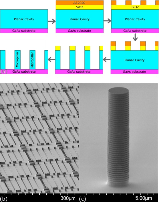
The samples were grown by molecular beam epitaxy. A high- cavity sample was grown consisting of a lower Bragg mirror of 26 pairs of alternating Al0.95Ga0.05As Cho et al. (2010) and GaAs layers, a single wavelength spacer with InAs QDs at its center, and a final 17 pair Bragg mirror. A low- cavity was also grown with 7/26 Bragg mirror pairs. The design wavelength was . The processing proceeds as shown in Fig. 1 (a) by coating the chips with a hard-mask layer of \ceSiO2 deposited via plasma enhanced chemical vapour deposition (PECVD). A layer of negative photo-resist, AZ2020, is applied and exposed using the MicroWriter ML3 Pro direct-write photo-lithography tool. The pattern consists of discs with diameters in the range to in regularly spaced arrays. This direct-write method allows for the patterning of devices in . After developing the photoresist in AZ726, the hard mask is etched using a C4F8/O2 inductively coupled plasma (ICP) and the photo-resist removed. The semiconductor is then etched using a Cl2/BCl3/N2 ICP. The hard mask is then removed with a second C4F8/O2 etch. Finally, the micropillars are encapsulated in a layer of Ta2O5 using atomic layer deposition. This oxide layer provides a uniform conformal coating that protects the samples against oxidation, especially for the DBR layers containing aluminium Tomm et al. (2021).
The quality of the patterning and semiconductor etch determines the sidewall roughness, which introduces losses to the cavity mode HE11 Schneider et al. (2016). The overall loss rate for photons in the mode is inversely proportional to the quality factor at a given diameter, , where the decay rate due to sidewall roughness is parameterized by , which adds to the loss rate through mirrors . can be determined from the -factor that cavities tend towards at high diameter. is linked to the diameter of the micropillar by the following expression , where is the sidewall loss coefficient, is the th order Bessel function with the transverse wavevector and the diameter Schneider et al. (2016).
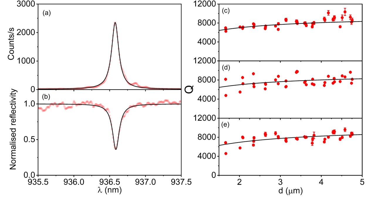
Two different techniques have been utilised to measure the cavity’s , photoluminescence (PL) and white light reflectivity (WLR), with example data shown in Fig. 2(a) and (b). The relatively high density of spectrally sharp QD transitions in the spectral range of the mode, made the measurement of using PL at unreliable. Therefore, the WLR measurement was used to determine the -factor of HE11 at this temperature, Fig. 2(c). Additionally, we measure the -factors at using PL (Fig. 2(d)) and WLR reflectivity (Fig. 2(e)). All three datasets yield a similar value for the sidewall loss coefficient , (c) of , (d) and (e) . These values are comparable to the state-of-the-art for these photonic structures Schneider et al. (2016) which reports .
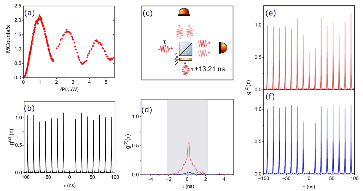
We then test the quantum light emission from these samples under resonant excitation. The sample was stored in air for three months after the processing with no observable degradation in . We study a neutral exciton on resonance with the HE11 in a diameter micropillar with a low -factor () and 7/26 Bragg mirror pairs. We focus on this sample because every pillar has transitions within broad cavity mode which can be resonantly excited. It has been show that these low cavities can be efficient and broadband Androvitsaneas et al. (2016); Ginés et al. (2022). The radiative lifetime of the transition is with a fine structure splitting of . Simulations suggest the maximum expected Purcell factor we could observe would be , with an overall expected efficiency of at the collection objective. Exciting the transition resonantly in a cross-polarized geometry Kuhlmann et al. (2013) we vary the pulse amplitude to observe a Rabi oscillation. With -pulse excitation the maximum count-rate is MHz, see Fig. 3(a). A second order autocorrelation measurement reveals the purity of the single photon emission Brown and Twiss (1954), when the system undergoes a full population inversion under the excitation of -pulse, to give , see Fig. 3(b).
Finally, we measure the indistinguishability of the single photons emitted under the conditions described above by interfering two sequentially emitted photons from the QD, Fig. 3(c). This yields a raw visibility of the two-photon interference Fig. 3(d-e). Based on the interferometer visibility and the value of the the overall corrected two photon interference visibility corresponds to Ollivier et al. (2021). This value is comparable to the visibility achieved with QDs in cavities with higher Purcell factors Arakawa and Holmes (2020); Somaschi et al. (2016); Ding et al. (2016); Wang et al. (2019); Tomm et al. (2021). This shows the excellent condition of the material even after the prolonged exposure to a non-controlled atmosphere.
This direct-write method can be used for high volume manufacturing of QD micropillar devices. The quality of the structure, low sidewall roughness, and high purity of the indistinguishable photons, shows its promise as a flexible platform for mass production of single photon sources. Future work could improve the collection efficiency into a single mode fiber by optimizing the far field emission pattern. An increased yield of optimized structures could be achieved by mapping the locations of dots prior to the processing, facilitating the repositioning of cavities and dots over a whole chip without the need for cryogenic lithography Dousse et al. (2008). Furthermore, with positioned arrays of QDs becoming available Große et al. (2020), the yield could approach unity.
Acknowledgements.
We acknowledge financial support provided by EPSRC via Grant No. EP/T017813/1 and EP/T001062/1. RC was supported by grant EP/S024441/1, Cardiff University and the National Physical Laboratory(NPL). We further thank Dr Alastair Sinclair and Dr Philip Dolan at NPL for technical discussions. Device processing was carried out in the cleanroom of the ERDF-funded Institute for Compound Semiconductors (ICS) at Cardiff University. For the purpose of open access, the author has applied a CC BY public copyright licence.Data Availability Statement
The data that support the findings of this study are available upon request.
References
References
- Arakawa and Holmes (2020) Y. Arakawa and M. J. Holmes, Applied Physics Reviews 7, 021309 (2020).
- Flagg et al. (2009) E. B. Flagg, A. Muller, J. Robertson, S. Founta, D. Deppe, M. Xiao, W. Ma, G. Salamo, and C.-K. Shih, Nature Physics 5, 203 (2009).
- Somaschi et al. (2016) N. Somaschi, V. Giesz, L. De Santis, J. Loredo, M. P. Almeida, G. Hornecker, S. L. Portalupi, T. Grange, C. Anton, J. Demory, et al., Nature Photonics 10, 340 (2016).
- Dousse et al. (2008) A. Dousse, L. Lanco, J. Suffczyński, E. Semenova, A. Miard, A. Lemaître, I. Sagnes, C. Roblin, J. Bloch, and P. Senellart, Physical review letters 101, 267404 (2008).
- Tomm et al. (2021) N. Tomm, A. Javadi, N. O. Antoniadis, D. Najer, M. C. Löbl, A. R. Korsch, R. Schott, S. R. Valentin, A. D. Wieck, A. Ludwig, et al., Nature Nanotechnology 16, 399 (2021).
- He et al. (2013) Y.-M. He, Y. He, Y.-J. Wei, D. Wu, M. Atatüre, C. Schneider, S. Höfling, M. Kamp, C.-Y. Lu, and J.-W. Pan, Nature nanotechnology 8, 213 (2013).
- Stevenson et al. (2006) R. M. Stevenson, R. J. Young, P. Atkinson, K. Cooper, D. A. Ritchie, and A. J. Shields, Nature 439, 179 (2006).
- Young et al. (2006) R. J. Young, R. M. Stevenson, P. Atkinson, K. Cooper, D. A. Ritchie, and A. J. Shields, New Journal of Physics 8, 29 (2006).
- Dousse et al. (2010) A. Dousse, J. Suffczyński, A. Beveratos, O. Krebs, A. Lemaître, I. Sagnes, J. Bloch, P. Voisin, and P. Senellart, Nature 466, 217 (2010).
- Basset et al. (2019) F. B. Basset, M. B. Rota, C. Schimpf, D. Tedeschi, K. D. Zeuner, S. C. Da Silva, M. Reindl, V. Zwiller, K. D. Jöns, A. Rastelli, et al., Physical Review Letters 123, 160501 (2019).
- Schwartz et al. (2016) I. Schwartz, D. Cogan, E. R. Schmidgall, Y. Don, L. Gantz, O. Kenneth, N. H. Lindner, and D. Gershoni, Science 354, 434 (2016).
- Lee et al. (2019) J. P. Lee, B. Villa, A. J. Bennett, R. M. Stevenson, D. J. P. Ellis, I. Farrer, D. A. Ritchie, and A. J. Shields, Quantum Science and Technology 4, 025011 (2019).
- Appel et al. (2022) M. H. Appel, A. Tiranov, S. Pabst, M. L. Chan, C. Starup, Y. Wang, L. Midolo, K. Tiurev, S. Scholz, A. D. Wieck, et al., Physical Review Letters 128, 233602 (2022).
- Ding et al. (2016) X. Ding, Y. He, Z. C. Duan, N. Gregersen, M. C. Chen, S. Unsleber, S. Maier, C. Schneider, M. Kamp, S. Höfling, C.-Y. Lu, and J.-W. Pan, Physical Review Letters 116, 020401 (2016).
- Wang et al. (2019) H. Wang, Y.-M. He, T.-H. Chung, H. Hu, Y. Yu, S. Chen, X. Ding, M.-C. Chen, J. Qin, X. Yang, R.-Z. Liu, Z.-C. Duan, J.-P. Li, S. Gerhardt, K. Winkler, J. Jurkat, L.-J. Wang, N. Gregersen, Y.-H. Huo, Q. Dai, S. Yu, S. Höfling, C.-Y. Lu, and J.-W. Pan, Nature Photonics 13, 770 (2019).
- Santori et al. (2002) C. Santori, D. Fattal, J. Vučković, G. S. Solomon, and Y. Yamamoto, Nature 419, 594 (2002).
- Bennett et al. (2016) A. J. Bennett, J. P. Lee, D. J. P. Ellis, I. Farrer, D. A. Ritchie, and A. J. Shields, Nature Nanotechnology 11, 857 (2016).
- Schneider et al. (2016) C. Schneider, P. Gold, S. Reitzenstein, S. Höfling, and M. Kamp, Applied Physics B 122, 19 (2016).
- Cho et al. (2010) N. Cho, K. Kim, J. Song, W. Choi, and J. Lee, Solid State Communications 150, 1955 (2010).
- Androvitsaneas et al. (2016) P. Androvitsaneas, A. B. Young, C. Schneider, S. Maier, M. Kamp, S. Höfling, S. Knauer, E. Harbord, C. Y. Hu, J. G. Rarity, and R. Oulton, Physical Review B 93, 241409 (2016).
- Ginés et al. (2022) L. Ginés, M. Moczała-Dusanowska, D. Dlaka, R. Hošák, J. R. Gonzales-Ureta, J. Lee, M. Ježek, E. Harbord, R. Oulton, S. Höfling, et al., Physical Review Letters 129, 033601 (2022).
- Kuhlmann et al. (2013) A. V. Kuhlmann, J. Houel, D. Brunner, A. Ludwig, D. Reuter, A. D. Wieck, and R. J. Warburton, Review of Scientific Instruments 84, 073905 (2013).
- Brown and Twiss (1954) R. H. Brown and R. Q. Twiss, The London, Edinburgh, and Dublin Philosophical Magazine and Journal of Science 45, 663 (1954).
- Ollivier et al. (2021) H. Ollivier, S. Thomas, S. Wein, I. M. de Buy Wenniger, N. Coste, J. Loredo, N. Somaschi, A. Harouri, A. Lemaitre, I. Sagnes, et al., Physical Review Letters 126, 063602 (2021).
- Große et al. (2020) J. Große, M. von Helversen, A. Koulas-Simos, M. Hermann, and S. Reitzenstein, APL Photonics 5, 096107 (2020).