Integrate and scale: A source of spectrally separable photon pairs
Abstract
Integrated photonics is a powerful contender in the race for a fault-tolerant quantum computer, claiming to be a platform capable of scaling to the necessary number of qubits. This necessitates the use of high-quality quantum states, which we create here using an all-around high-performing photon source on an integrated photonics platform. We use a photonic molecule architecture and broadband directional couplers to protect against fabrication tolerances and ensure reliable operation. As a result, we simultaneously measure a spectral purity of %, a pair generation rate of MHz mW-2, and an intrinsic source heralding efficiency of %. We also see a maximum coincidence-to-accidental ratio of . We claim over an order of magnitude improvement in the trivariate trade-off between source heralding efficiency, purity and brightness. Future implementations of the source could achieve in excess of purity and heralding efficiency using state-of-the-art propagation losses.
I Introduction
Progress toward practical quantum computational platforms is accelerating, with increasing competition from various industrial efforts [1, 2, 3, 4]. Quantum computers promise the ability to efficiently simulate complex quantum systems [5, 6], solve classically infeasible cryptography challenges [7], and make possible revolutionary low-carbon technologies [8] amongst other applications. This is in direct contrast to the lengthy and comparatively inefficient computations of our classical methodologies [9]. Quantum photonics is one such platform, and further benefits from its mass-manufacturability (integrated photonics) on chip-scale devices [10, 11]. From an applications perspective, it enables the likes of large-scale entangled quantum networks [12, 13], next-generation sensing [14], and ultra-precise measurements [15]. The integrated photonics platform grows ever more promising with the developments of many fundamental building blocks needed for a photonic quantum computer [16, 17, 18, 19, 20, 21], and is possibly the only platform capable of reaching the number of qubits necessary for true fault-tolerance [22].
Much of the theory surrounding a photonic quantum processor postulates ideal quantum resources [23] for the purposes of their architecture [24, 25], as well as for any error-correction schemes [26, 27, 28]. To create a photon source in line with these requirements we need high heralding efficiencies and high purities. High brightness sources are more of a practical requirement, as brightness determines the time frame on which a given computation can be performed [18], with larger circuits needing brighter sources to maintain similar coincidence rates. Together, these metrics maximize the generation probability of sources; which is key for interfering photons from multiple sources, as well as maximizing any subsequent interference between them, making results like [29] achievable. Recent examples targeting improved integrated source metrics showcase versatile [30], and bright sources [31] of indistinguishable photons with limited heralding efficiency, or high-efficiency sources that trade brightness for purity, and are limited to broadband operation [16] leaving them susceptible to additional noise inside the wider filtering band.
Typically, the nonlinear process of spontaneous four-wave mixing (SFWM) is used to probabilistically generate pairs of photons (conventionally referred to as signals and idlers) on the CMOS-compatible silicon-on-insulator (SOI) platform. Devices can be designed to optimize the brightness of this process through long interaction lengths; manifesting as long sections of waveguide [32], or high-field strengths in optical cavities [33] which can more easily result in lower escape efficiencies [34]. These sources use the process of heralding [35] to mitigate the probabilistic nature of SFWM, with valid detection events occurring only with two or more coincident photons. The consequence of heralding is that, due to the energy and momentum-conserving nature of SFWM, any correlation between signal and idler photons projects the heralded photon into a mixed state. The heralded generation of entangled states [36] relies on the interference of multiple indistinguishable photons, and if the heralded single-photons are in a mixed state, this will degrade any quantum interference between them [37].
Here we showcase a photon-pair source using the resonantly enhanced SFWM process to maximize brightness and spectral purity, additionally, design optimizations of a photonic molecule architecture promise heralding efficiencies much higher than previously demonstrated for ring resonators. Our source comes with built-in resilience to fabrication variations to help ensure that these devices can be fabricated identically with high yields. The inevitable target will be to use large banks of these sources in parallel. This resilience comes in part from the strong-coupling regime that we operate in, but equally from our directional coupler designs. Motivated by previous works [38, 39], and using the transfer matrix method (TMM), we chose device geometries expected to offer broadband operation, and fabrication resilience, something that has been proposed [38] but never implemented in a full device to the knowledge of the authors.
II Design
Simple ring resonators are bound to purities of up to 91.7% due to strict energy conservation conditions between identical linewidth resonances [40, 41]. However, this limit can be alleviated if the pump resonance linewidth is broadened relative to the signal/idler fields as in [41, 31], or alternatively, if the temporal response of the pump is sharpened [42, 30]. Reducing the interaction length or amplitude of the pump field in any way will lead to a predictable decay in the brightness of the SFWM process [41, 42].
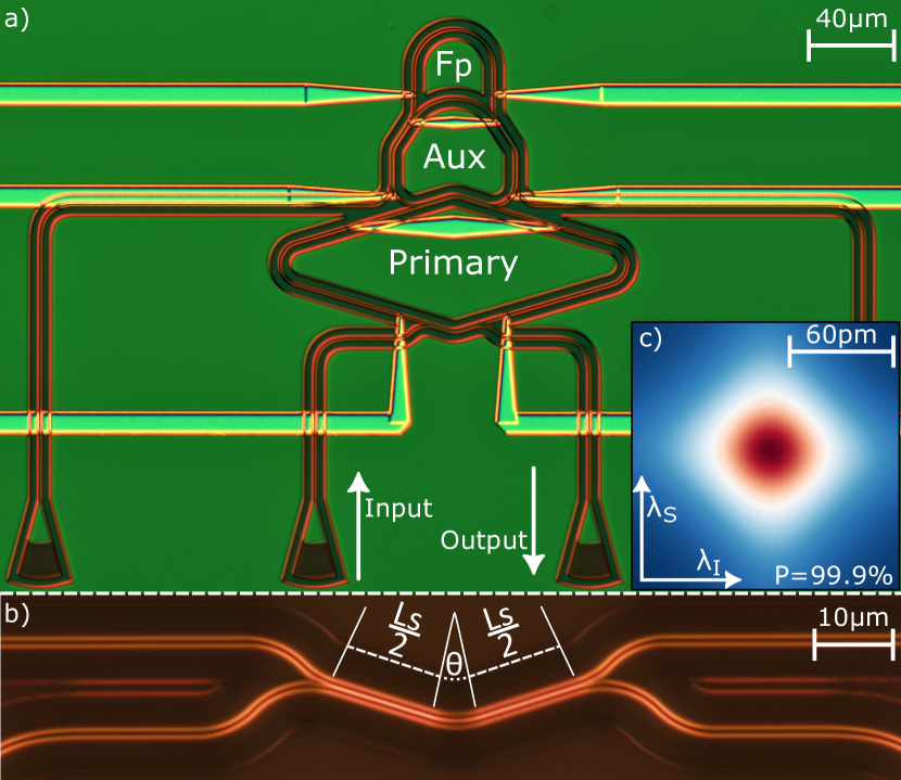
Figure. 1a shows our resonator-based photon source design that allows us to engineer the spectral response of the in-resonator pump fields compared to those of the signal/idlers. The coupled resonators (primary-auxiliary) mean that we engineer only the shared resonances between the rings, and restrict photon generation solely to the primary resonator. Promisingly, the idea of a photonic molecule has already proved a versatile and auspicious design [43, 44, 45]. Here, our control over the in-resonator pump spectrum comes from the inter-resonator coupling between our primary resonator, which is simultaneously resonant at all three wavelengths of interest (signal, idler, and pump), and our auxiliary resonator which is solely resonant at our pump wavelength. Additionally, we implement a loss channel (Fp) for only the pump wavelengths using an asymmetric Mach-Zehnder interferometer (AMZI) to avoid inducing excess loss for the signal/idler photons. As part of the auxiliary resonator, Fp provides control over the auxiliary resonance linewidth and hence, control over the lineshape of the pump in the primary resonator, and for the purposes of source brightness, its field enhancement. In expanding the possible resonant lineshapes of our pump beyond that of a simple Lorentzian [46], we aim to reduce the trivariate trade-off between purity, brightness, and heralding efficiency that is prominently discussed in previous works [34, 41, 42].
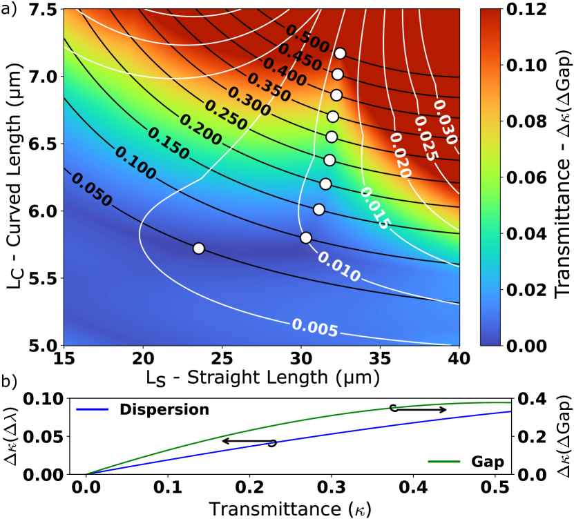
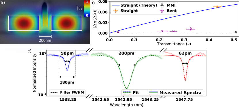
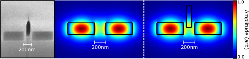
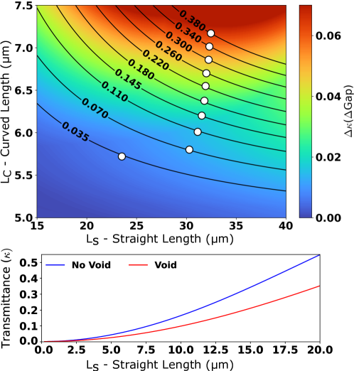
The platform chosen for this work uses waveguide geometries of 500 x 220 nm, and a bend-radius of 10 m as a compromise between footprint and bend-losses, with estimated propagation losses of 5 dB/cm. This allows our source to fit inside a footprint of 143 m x 172 m. In assessing the sensitivity of straight-directional couplers () to both wavelength and fabrication variations (specifically waveguide separations of 50 nm), we saw that higher transmittance lead to increased sensitivity in both categories (Fig. 2b). This is in stark contrast to the design space of the bent couplers (Fig. 2a) where both wavelength and fabrication sensitivity can be minimized by choosing a specific geometry of coupler. For our bent couplers, we chose a waveguide separation of 200 nm to minimize their footprint, as well as their wavelength and fabrication sensitivity.
III Results and Discussion
III.1 Robustness
Any practical photon-pair source must retain its mass-fabricability, and as such, it needs to be resilient to fabrication inaccuracies. The intrinsic design of our source plays a major role in its robustness as targeting higher heralding efficiency using a ring-resonator necessitates operating in the strongly over-coupled regime [34], which, if targeting an all-around high-performance photon source, is one of many constraints we need to operate within. This regime comes with inherent tolerance to fabrication as small deviations will proportionally impact the design less. In particular, without Fp we would have to work with very small, and therefore sensitive couplings between the primary and auxiliary resonator. This is analogous to the limited purity gains (97%) from a small amount of pump backscattering in ring resonators [46], in our design Fp allows us to work with much higher inter-ring coupling strengths, and also leads to higher purities (see Supplement 1).
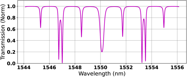
As for the couplers themselves, SEM images of the devices (Fig. 3a) highlighted the limitations of the fabrication technology and confirmed the anticipated presence of voids (absence of cladding). Voids are a common issue when depositing thick films using chemical vapor deposition (CVD) on structures with aspect ratios larger than 1:1, and the likelihood of voids is increased inside devices with small waveguide separations [47]. Accordingly, this can be alleviated by reducing the aspect ratio of the coupling region (ratio of waveguide height and separation — [48]), which is a means of adding some fabrication tolerance to straight directional couplers at the cost of device footprint. Regardless, we can infer their robustness by characterizing the coupler test structures across the chip that are located on average 2.9 mm apart to ensure no local correlations (Fig. 3b). Our devices for comparison were a straight directional coupler and a standard multimode interferometer (MMI) both for 3 dB splitting at 1550 nm. We measured each device’s transmission across the telecom c-band to test their performance and saw almost negligible dispersion compared to a straight coupler (Fig. 3b). Each coupler performed well with a small spread in transmittance across the chip which fell within expectations (Fig. 2a) and the dispersion of each coupler continued to compete with that of an MMI (Fig. 3b). This is further evident in the spectrum of the photonic molecule (Fig. 3c — full spectra in Supplement 1), where over 10 nm we see very little change in the linewidth of the resonances. Interestingly, the straight coupler’s transmittance is lower than expected for the device, which could still be explained by a cladding void that forms later in the PECVD process.
III.2 Brightness
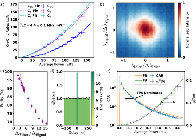
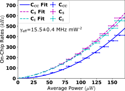
We experimentally characterized our photon-pair source by pumping it with a 340 pm (9 ps) bandwidth pulsed laser at a 51 MHz repetition rate, to excite the pump resonance of the ring which has a bandwidth of 200 pm (Fig. 3c). To estimate source brightness we varied the power of the pulsed laser on-chip using a variable optical attenuator (VOA) and measured the dependence of coincidences and singles with on-chip power. On-chip average power was estimated using a 90:10 fiber coupler, and the insertion loss of our grating couplers (3.8dB — see Supplement 1). We kept the pump power low to avoid excess nonlinear loss from two-photon absorption (TPA, [49]) which is annotated in Figure. 4e where the expected coincidence-to-accidental ratio (CAR) deviates from the ideal fit at about 0.15 mW. We can solve for heralding efficiencies at the detectors and the effective nonlinearity () by quadratically fitting the singles and coincidence rates (Fig. 4a — Supplement 1). The that we extract is 4.4 0.1 MHz mW-2. The effective nonlinearity essentially characterizes the on-chip generation rate, and therefore the brightness of the photon-pair source. By performing a similar measurement after taking the auxiliary ring off-resonance, we see that jumps to 15.5 0.4 MHz mW-2 (see Supplement 1). This 3.5x increase in brightness translates to a mere 1.9x increase in peak power delivered to the photonic molecule to achieve the same rates. Comparatively, [41] predicts that for our resonant setup, we would see a 46x decrease in brightness, corresponding to a 6.8x increase in peak power to recover the same generation rate of a single ring, demonstrating the power of our design with over an order of magnitude improvement in the expected brightness.
III.3 Purity
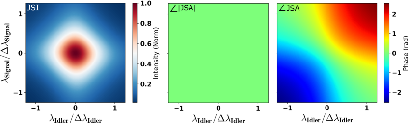
We characterized the source spectral purity using stimulated emission tomography (SET — [50]) to extract the joint spectral intensity (JSI) of the photon-pair source, followed by a Schmidt decomposition on the corresponding joint spectral amplitude (JSA) to obtain an estimate of spectral purity. Additionally, we took measurements of the unheralded second-order correlation function ( — [51]) to corroborate our estimate of purity. The heralded is an additional metric that quantifies the photon-number purity and is due to the probabilistic nature of SFWM combined with our non-photon-number resolving detection. It is related to the likelihood of producing more than one photon pair in a single coincidence window. For our SET measurements, we used a continuous-wave (CW — T100S-HP) laser with a linewidth of 3.2 to perform a wavelength scan (1 resolution) over the signal resonance, measuring the output power at the idler resonance using a high-resolution (0.16 ) optical spectrum analyzer (OSA — Waveanalyzer 1500s). The result of this measurement is presented in Figure. 4b, and the corresponding purity is 99.1 0.1, in-line with the predictions of [41] and unequivocally demonstrating the unentangled nature of our photons. While the JSI discards phase information of the JSA, previous works [30] have reported that for high-purity JSIs, the purity estimate of the JSI converges with that of the true JSA, for which our simulations suggest a difference of only (see Supplement 1). To obtain the error on our JSI measurement, we used a supersampling technique to take advantage of the huge precision afforded to us by our equipment, allowing us to reduce the effect of noise from both our OSA and our tunable CW laser. This reduced the uncertainty in our measurement, and at a final resolution of 4 , plateaued in both error and purity (see Supplement 1), allowing us to say with confidence that our measurement contains the true value of purity.
While measurements can be subject to more noise due to its unheralded nature [52], it can serve to verify a source’s spectral purity in a scenario more closely resembling a realistic use-case. We pass our pump through a 400 bandwidth filter to ensure no excess noise contaminates our measurement. Taking our signal photons, we filter them to varying degrees using the tunable filter, send them into a 50:50 fiber beamsplitter, and measure the CAR between the two arms of the beamsplitter. This ratio should be 2 if the photon is in a pure state, i.e. exhibiting perfect thermal statistics. Our results are shown in Figure. 4c. The best measured is 1.98 0.02 for a filter bandwidth twice as wide as our source, which ensures the highest removal of any broadband nonlinear noise surrounding the source due to the 100 of waveguide either side of our source. We chose this length of input waveguide to provide a practical estimate of how this source could perform as part of a larger circuit according to our other works [53]. However, finding the best compromise between noise removal and filter bandwidth () we observe a of 1.97 0.02 (Fig. 4d) where we measure our highest CAR between signal and idler photons of 1644 263 (Fig. 4e). Only filtering to this extent also avoids any serious degradation of the heralding efficiency which becomes an issue for filters approaching the bandwidth of the source [54]. This measurement agrees with that of our measured JSI and further certifies the purity of our photons. Finally, we measure a minimum value of 0.0029 0.0021 (Fig. 4e), well inside the single photon regime.
III.4 Efficiency
To get the best idea of the source’s full efficiency we use a filtering bandwidth of 500 pm. The heralding efficiency that we measure off-chip is = 7.2 0.2 , and = 5.6 0.2 , where indicate the efficiencies of the signal and idler photons, respectively. However, we care more about the intrinsic heralding efficiency of the source, because that is the limiting factor for any on-chip implementation of single-photon detectors, which would remove coupling-related insertion losses. We tally up the losses of our setup by measuring the insertion loss from the output of our laser power reference to our detectors both with and without the chip to isolate the insertion loss of the signal and idler channels. Most of our losses come from our filtering (See Supplement 1), which adds insertion losses of approximately 6 dB in total and consists of a fiber DWDM (1 bandwidth) for coarse filtering, and more noise-isolating filtering using a tunable filter (XTA-50). Additionally, we have characterization data from the detectors we are using to be able to account for non-unity detection efficiencies equivalent to insertion losses of -1.060 0.044 dB, and -0.814dB 0.026 dB (See Supplement 1). After this analysis, the post-source heralding efficiencies that we estimate are = 92.1 3.2 , and = 94.0 2.9 , which is extremely competitive even with waveguide implementations of next-generation sources ( = 91 9 — [16]).
IV Conclusions
The photonic molecule architecture of our photon-pair source brings clear gains in all of the key metrics that are required to build a fault-tolerant photonic quantum computer. Our measured purities of 99.1 0.1, certified using measurements, are fundamental in the creation of quantum resources through entangling operations [2]. Additionally, with a competitive maximum measured heralding efficiency of 94.0 2.9 , especially when compared to previously reported pure resonators ( = 52.4 — [31]), our source successfully operates within on-chip loss thresholds of a fusion-based architecture [24]. Our source surpasses expectations set by previous works [30, 42, 31, 41], and reduces the trade-off between brightness, heralding efficiency, and purity, with a measured = 4.4 0.1 MHz mW-2, beating expected brightness degradation by over an order of magnitude [41]. Finally, our source is reasonably resilient fabrication defects (Fig. 3a) and variances, both through the implementation of fabrication-tolerant directional couplers with dramatically reduced dispersion, and the intrinsic over-coupled design of our source. Therefore, our results present the brightest, most efficient ring resonator source of pure photons to date, that has scalability at the core of its design. State-of-the-art propagation losses [17] could improve source heralding efficiencies to values in excess of 99. The full power of our design can therefore be realized through the maturity of the fabrication process as all of our source metrics can only improve with reduced propagation losses due to higher Q-factors [34], leading to a scalable and truly optimizable source.
V Acknowledgments
B.M.B. would like to thank Massimo Borghi, Will McCutcheon, and Gary Sinclair for useful discussions. The authors would like to thank Andy Murray for their technical assistance, as well as Laurent Kling and Stefano Paesani for their work characterising the efficiency of the detectors. The authors would also like to thank the team at CORNERSTONE, including Callum Littlejohns, Ying Tran, Mehdi Banakar, Martin Ebert, James Le Besque, Georgia Mourkioti, and Eleni Tsanidou for their technical assistance and SEM imaging of our devices. The chip used in this work was fabricated using the facilities available at CORNERSTONE.
VI Funding
B.M.B. acknowledges the support of the EPSRC training grant EP/LO15730/1. The authors acknowledge the support of the EPSRC Quantum Communications Hub (EP/T001011/1) and Quantum Photonic Integrated Circuits (QuPIC) (EP/N015126/1). The authors also include the use of a paid MPW service CORNERSTONE 2 (EP/T019697/1).
VII Supplemental document
See Supplement 1 for supporting content.
References
- Bourassa et al. [2021] J. E. Bourassa, R. N. Alexander, M. Vasmer, A. Patil, I. Tzitrin, T. Matsuura, D. Su, B. Q. Baragiola, S. Guha, G. Dauphinais, et al., Blueprint for a scalable photonic fault-tolerant quantum computer, Quantum 5, 392 (2021).
- Bartolucci et al. [2021a] S. Bartolucci, P. M. Birchall, M. Gimeno-Segovia, E. Johnston, K. Kieling, M. Pant, T. Rudolph, J. Smith, C. Sparrow, and M. D. Vidrighin, Creation of entangled photonic states using linear optics, arXiv preprint arXiv:2106.13825 (2021a).
- Egan et al. [2021] L. Egan, D. M. Debroy, C. Noel, A. Risinger, D. Zhu, D. Biswas, M. Newman, M. Li, K. R. Brown, M. Cetina, et al., Fault-tolerant control of an error-corrected qubit, Nature 598, 281 (2021).
- Arute et al. [2019] F. Arute, K. Arya, R. Babbush, D. Bacon, J. C. Bardin, R. Barends, R. Biswas, S. Boixo, F. G. Brandao, D. A. Buell, et al., Quantum supremacy using a programmable superconducting processor, Nature 574, 505 (2019).
- McArdle et al. [2020] S. McArdle, S. Endo, A. Aspuru-Guzik, S. C. Benjamin, and X. Yuan, Quantum computational chemistry, Reviews of Modern Physics 92, 015003 (2020).
- Abrams and Lloyd [1997] D. S. Abrams and S. Lloyd, Simulation of many-body fermi systems on a universal quantum computer, Physical Review Letters 79, 2586 (1997).
- Shor [1999] P. W. Shor, Polynomial-time algorithms for prime factorization and discrete logarithms on a quantum computer, SIAM review 41, 303 (1999).
- Delgado et al. [2022] A. Delgado, P. A. M. Casares, R. dos Reis, M. S. Zini, R. Campos, N. Cruz-Hernández, A.-C. Voigt, A. Lowe, S. Jahangiri, M. A. Martin-Delgado, J. E. Mueller, and J. M. Arrazola, Simulating key properties of lithium-ion batteries with a fault-tolerant quantum computer, Phys. Rev. A 106, 032428 (2022).
- Feynman [1982] R. P. Feynman, Simulating physics with computers, International Journal of Theoretical Physics 21, 467 (1982).
- Wang et al. [2020] J. Wang, F. Sciarrino, A. Laing, and M. G. Thompson, Integrated photonic quantum technologies, Nature Photonics 14, 273 (2020).
- Moody et al. [2022] G. Moody, V. J. Sorger, D. J. Blumenthal, P. W. Juodawlkis, W. Loh, C. Sorace-Agaskar, A. E. Jones, K. C. Balram, J. C. Matthews, A. Laing, et al., 2022 roadmap on integrated quantum photonics, Journal of Physics: Photonics 4, 012501 (2022).
- Joshi et al. [2020] S. K. Joshi, D. Aktas, S. Wengerowsky, M. Lončarić, S. P. Neumann, B. Liu, T. Scheidl, G. C. Lorenzo, Ž. Samec, L. Kling, et al., A trusted node–free eight-user metropolitan quantum communication network, Science advances 6, eaba0959 (2020).
- Wengerowsky et al. [2018] S. Wengerowsky, S. K. Joshi, F. Steinlechner, H. Hübel, and R. Ursin, An entanglement-based wavelength-multiplexed quantum communication network, Nature 564, 225 (2018).
- Titchener et al. [2022] J. Titchener, D. Millington-Smith, C. Goldsack, G. Harrison, A. Dunning, X. Ai, and M. Reed, Single photon lidar gas imagers for practical and widespread continuous methane monitoring, Applied Energy 306, 118086 (2022).
- Giovannetti et al. [2004] V. Giovannetti, S. Lloyd, and L. Maccone, Quantum-enhanced measurements: beating the standard quantum limit, Science 306, 1330 (2004).
- Paesani et al. [2020] S. Paesani, M. Borghi, S. Signorini, A. Maïnos, L. Pavesi, and A. Laing, Near-ideal spontaneous photon sources in silicon quantum photonics, Nature communications 11, 1 (2020).
- Biberman et al. [2012] A. Biberman, M. J. Shaw, E. Timurdogan, J. B. Wright, and M. R. Watts, Ultralow-loss silicon ring resonators, Optics letters 37, 4236 (2012).
- Meyer-Scott et al. [2020] E. Meyer-Scott, C. Silberhorn, and A. Migdall, Single-photon sources: Approaching the ideal through multiplexing, Review of Scientific Instruments 91, 041101 (2020).
- Eltes et al. [2020] F. Eltes, G. E. Villarreal-Garcia, D. Caimi, H. Siegwart, A. A. Gentile, A. Hart, P. Stark, G. D. Marshall, M. G. Thompson, J. Barreto, et al., An integrated optical modulator operating at cryogenic temperatures, Nature Materials 19, 1164 (2020).
- Chang et al. [2021] J. Chang, J. Los, J. Tenorio-Pearl, N. Noordzij, R. Gourgues, A. Guardiani, J. Zichi, S. Pereira, H. Urbach, V. Zwiller, et al., Detecting telecom single photons with 99.5- 2.07+ 0.5% system detection efficiency and high time resolution, APL Photonics 6, 036114 (2021).
- Reddy et al. [2020] D. V. Reddy, R. R. Nerem, S. W. Nam, R. P. Mirin, and V. B. Verma, Superconducting nanowire single-photon detectors with 98% system detection efficiency at 1550 nm, Optica 7, 1649 (2020).
- Rudolph [2017] T. Rudolph, Why i am optimistic about the silicon-photonic route to quantum computing, APL photonics 2, 030901 (2017).
- Li et al. [2022] B. Li, S. E. Economou, and E. Barnes, Photonic resource state generation from a minimal number of quantum emitters, npj Quantum Information 8, 1 (2022).
- Bartolucci et al. [2021b] S. Bartolucci, P. Birchall, H. Bombin, H. Cable, C. Dawson, M. Gimeno-Segovia, E. Johnston, K. Kieling, N. Nickerson, M. Pant, et al., Fusion-based quantum computation, arXiv preprint arXiv:2101.09310 (2021b).
- Raussendorf and Briegel [2001] R. Raussendorf and H. J. Briegel, A one-way quantum computer, Physical review letters 86, 5188 (2001).
- Kitaev [2003] A. Kitaev, Fault-tolerant quantum computation by anyons, Annals of Physics 303, 2 (2003).
- Shor [1995] P. W. Shor, Scheme for reducing decoherence in quantum computer memory, Phys. Rev. A 52, R2493 (1995).
- Schlingemann and Werner [2001] D. Schlingemann and R. F. Werner, Quantum error-correcting codes associated with graphs, Physical Review A 65, 012308 (2001).
- Zhong et al. [2020] H.-S. Zhong, H. Wang, Y.-H. Deng, M.-C. Chen, L.-C. Peng, Y.-H. Luo, J. Qin, D. Wu, X. Ding, Y. Hu, et al., Quantum computational advantage using photons, Science 370, 1460 (2020).
- Burridge et al. [2020] B. M. Burridge, I. I. Faruque, J. G. Rarity, and J. Barreto, High spectro-temporal purity single-photons from silicon micro-racetrack resonators using a dual-pulse configuration, Optics Letters 45, 4048 (2020).
- Liu et al. [2020] Y. Liu, C. Wu, X. Gu, Y. Kong, X. Yu, R. Ge, X. Cai, X. Qiang, J. Wu, X. Yang, et al., High-spectral-purity photon generation from a dual-interferometer-coupled silicon microring, Optics Letters 45, 73 (2020).
- Wang et al. [2018] J. Wang, S. Paesani, Y. Ding, R. Santagati, P. Skrzypczyk, A. Salavrakos, J. Tura, R. Augusiak, L. Mančinska, D. Bacco, et al., Multidimensional quantum entanglement with large-scale integrated optics, Science 360, 285 (2018).
- Llewellyn et al. [2020] D. Llewellyn, Y. Ding, I. I. Faruque, S. Paesani, D. Bacco, R. Santagati, Y.-J. Qian, Y. Li, Y.-F. Xiao, M. Huber, et al., Chip-to-chip quantum teleportation and multi-photon entanglement in silicon, Nature Physics 16, 148 (2020).
- Vernon et al. [2016] Z. Vernon, M. Liscidini, and J. E. Sipe, No free lunch: the trade-off between heralding rate and efficiency in microresonator-based heralded single photon sources, Optics letters 41, 788 (2016).
- Hong and Mandel [1986] C. Hong and L. Mandel, Experimental realization of a localized one-photon state, Physical Review Letters 56, 58 (1986).
- Barz et al. [2010] S. Barz, G. Cronenberg, A. Zeilinger, and P. Walther, Heralded generation of entangled photon pairs, Nature photonics 4, 553 (2010).
- Sinclair and Thompson [2016] G. F. Sinclair and M. G. Thompson, Effect of self-and cross-phase modulation on photon pairs generated by spontaneous four-wave mixing in integrated optical waveguides, Physical Review A 94, 063855 (2016).
- Morino et al. [2014] H. Morino, T. Maruyama, and K. Iiyama, Reduction of wavelength dependence of coupling characteristics using si optical waveguide curved directional coupler, Journal of lightwave technology 32, 2188 (2014).
- Chen et al. [2017] G. F. Chen, J. R. Ong, T. Y. Ang, S. T. Lim, C. E. Png, and D. T. Tan, Broadband silicon-on-insulator directional couplers using a combination of straight and curved waveguide sections, Scientific reports 7, 1 (2017).
- Helt et al. [2010] L. G. Helt, Z. Yang, M. Liscidini, and J. E. Sipe, Spontaneous four-wave mixing in microring resonators, Optics letters 35, 3006 (2010).
- Vernon et al. [2017] Z. Vernon, M. Menotti, C. Tison, J. Steidle, M. Fanto, P. Thomas, S. Preble, A. Smith, P. Alsing, M. Liscidini, et al., Truly unentangled photon pairs without spectral filtering, Optics letters 42, 3638 (2017).
- Christensen et al. [2018] J. B. Christensen, J. G. Koefoed, K. Rottwitt, and C. McKinstrie, Engineering spectrally unentangled photon pairs from nonlinear microring resonators by pump manipulation, Optics letters 43, 859 (2018).
- Borghi et al. [2019] M. Borghi, A. Trenti, and L. Pavesi, Four wave mixing control in a photonic molecule made by silicon microring resonators, Scientific reports 9, 1 (2019).
- Gentry et al. [2014] C. M. Gentry, X. Zeng, and M. A. Popović, Tunable coupled-mode dispersion compensation and its application to on-chip resonant four-wave mixing, Optics letters 39, 5689 (2014).
- Gentry et al. [2016] C. M. Gentry, G. T. Garcés, X. Zeng, and M. A. Popović, Tailoring of individual photon lifetimes as a degree of freedom in resonant quantum photonic sources, in CLEO: Applications and Technology (Optica Publishing Group, 2016) pp. JTu5A–17.
- McCutcheon [2021] W. McCutcheon, Backscattering in nonlinear microring resonators via a gaussian treatment of coupled cavity modes, APL Photonics 6, 066103 (2021).
- Foggiato [2001] J. Foggiato, Chemical vapor deposition of silicon dioxide films, in Handbook of Thin Film Deposition Processes and Techniques (Elsevier, 2001) pp. 111–150.
- Schwartz and Johns [1992] G. C. Schwartz and P. Johns, Gap-fill with pecvd sio2 using deposition/sputter etch cycles, Journal of the Electrochemical Society 139, 927 (1992).
- Husko et al. [2013] C. A. Husko, A. S. Clark, M. J. Collins, A. De Rossi, S. Combrié, G. Lehoucq, I. H. Rey, T. F. Krauss, C. Xiong, and B. J. Eggleton, Multi-photon absorption limits to heralded single photon sources, Scientific reports 3, 1 (2013).
- Liscidini and Sipe [2013] M. Liscidini and J. Sipe, Stimulated emission tomography, Physical review letters 111, 193602 (2013).
- Christ et al. [2011] A. Christ, K. Laiho, A. Eckstein, K. N. Cassemiro, and C. Silberhorn, Probing multimode squeezing with correlation functions, New Journal of Physics 13, 033027 (2011).
- Faruque et al. [2019] I. I. Faruque, G. F. Sinclair, D. Bonneau, T. Ono, C. Silberhorn, M. G. Thompson, and J. G. Rarity, Estimating the indistinguishability of heralded single photons using second-order correlation, Physical Review Applied 12, 054029 (2019).
- Burridge et al. [2022] B. M. Burridge, I. I. Faruque, J. G. Rarity, and J. Barreto, Quantifying hidden nonlinear noise in integrated photonics, arXiv preprint arXiv:2209.14317 (2022).
- Meyer-Scott et al. [2017] E. Meyer-Scott, N. Montaut, J. Tiedau, L. Sansoni, H. Herrmann, T. J. Bartley, and C. Silberhorn, Limits on the heralding efficiencies and spectral purities of spectrally filtered single photons from photon-pair sources, Physical Review A 95, 061803 (2017).
Integrate and scale: A source of spectrally separable photon pairs
—– Supplemental Material —–
VIII Modal Simulations of Directional Couplers
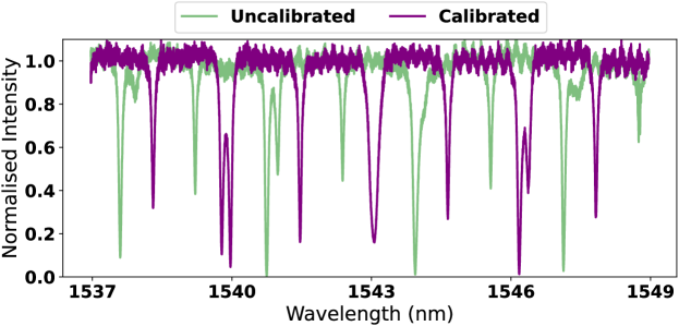
The methodology for the simulations of the bent directional coupler directly follows from the work in [39], and uses the transfer matrix method (TMM) to work out the final transmittance of a given coupler. To do this, we must solve the modes for each section of the directional coupler, meaning 6 solutions in total, 2 for each section (single waveguides, straight section, bent section). In doing this we construct the simulated waveguides exactly as we expect them to be fabricated. The benefit of this is that very quickly we have access to the transmittance of any bent directional coupler within a range of straight and curved lengths (). However, if the fabricated waveguides differ in some way, then of course the simulation will not accurately re-produce their real-world performance. This is where we have used SEM images of the devices provided by CORNERSTONE to give us as accurate a picture as possible for post-fabrication analysis. In these images, we observed the presence of cladding voids in the coupling region of our device (Fig. S1)
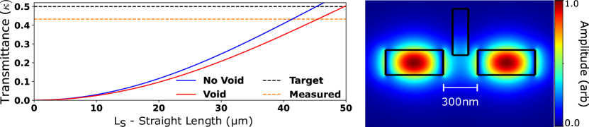
Solving for all of the modes using this new waveguide assembly, we saw that the performance of the bent couplers, while expected to be lower, was not so low as to be catastrophic. Especially when compared to straight directional couplers with a similar waveguide separation (Fig. S2). When designing straight directional couplers for this chip, we used a waveguide separation of 300 nm for an added degree of fabrication tolerance. Looking at simulations of a cladding void in the centre of these couplers, they do seem to have a diminished effect (Fig. S1). The behavior of Fig. S3 does a good job of explaining the underperformance of our straight coupler as mentioned in the main text.
IX Design Optimizations of a Photonic Molecule
To effectively simulate our photonic molecule, first, we must solve our system of ring resonators to work out their transmission spectra and corresponding field enhancements. These field enhancements can be used to work out the performance of our source, as usual, [40].
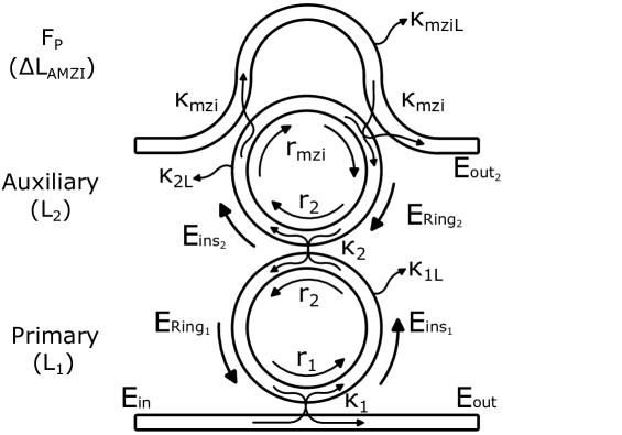
Our ring system can be schematically drawn as in Figure. S4, and we can start our modelling similarly to the single-ring case. For the primary-bus coupling junction, we have
| (1) |
where for simplicity is the field before the coupling region . We can write a similar set of equations for the primary-auxiliary coupling
| (2) |
where is the ring self-coupling due to the loss channel as before. Finally, we can write another set of equations for the -auxiliary coupling
| (3) |
where we have assumed no light enters the structure other than from , and for simplicity have concatenated the relative phase of using the path-difference . Now we can begin solving this system of equations, starting with Eq. 3
| (6) |
such that
| (7) |
At this point, I will define to represent the complex round-trip transmission of the auxiliary ring. Letting us re-write Eq. 7 as
| (8) |
where the only unknown remaining is which we can now solve using Eq. 2
| (9) |
which we can re-arrange to get
| (10) |
Finally, using Eq. 1 we can work out the transmitted field of the photonic molecule as
| (11) |
which is given by
| (12) |
With a complete model, we can move on to simulating the performance of different designs of the photonic molecule.
In designing our photonic molecule, the parameter we wanted to constrain ourselves with first was heralding efficiency. We can choose heralding efficiency using only one parameter, the ring-bus coupling of the primary resonator [34]. This necessitated working in the strong coupling regime, giving rise to our relatively broad 60 pm resonances of the primary resonator. By setting this constraint earlier, we only have a 2D parameter space to explore, which is the transmittance of the couplers used inside Fp, and the primary-auxiliary ring coupling. Scanning these parameters allows us to quickly decide on an optimal photonic molecule for a given operating scenario (Fig. S5).
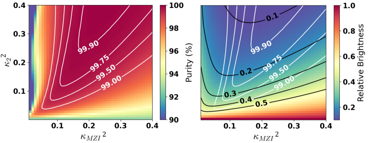
We mentioned in the main text that the use of Fp allowed us to operate with higher coupling strengths, and this can be seen in Fig. S5. Additionally, the features on these optimization plots are slowly varying at higher coupling strengths which highlight the fabrication tolerance of this particular source architecture. We can also make inferences about the brightness of our device. Given a single ring that operates at a brightness around an easily achievable 10 MHz, we maintain MHz rates well into the 99.9% purity regime. Our source operates at a relative brightness of 0.28 that of a single ring, which is close to predicted.
X Brightness Measurements of a Photon-Pair Source
To measure the brightness of our source, we correlate the rate of singles for each channel with the total true coincidence rate. We can do this based on our knowledge of the system, in that coincidence events () occur between two photons of a pair through spontaneous four-wave mixing or random chance (accidentals – ), single photon detections can come from SFWM events () and random linear noise which can be a result of pump leakage or other scattering events. Dark count rates () of the detectors will also act as a constant offset to single photon detection rates. Using this knowledge, we fit the brightness curves using the equations
| (13) | |||
| (14) | |||
| (15) | |||
| (16) |
where is the brightness or effective nonlinearity of our pair source in Hz mW-2. The lumped linear noise coefficient for each channel is represented using , and is the on-chip pump power. These equations also allow us to extract the total heralding efficiency of the signal () and the idler () channels. In simpler terms, it is the on-chip pair generation rate (PGR), at 1 mW. The pair generation rate is our main point of comparison between sources, but PGR can be specified at any on-chip power, which then needs to be scaled appropriately for comparison. Finally, the accidentals () can be estimated from the detected singles rates as in Eq. 16 over the coincidence window () or, more typically, are calculated from the measured coincidence data.
As mentioned in the main text, we also measured the brightness of the source if we took the auxiliary ring off-resonance, which gave us an estimate of the single-ring brightness of our particular setup. We measured the in this case to be 15.5 0.4 MHz mW-2 (Fig. S8) as mentioned in the main text. Fitting each of the curves according to Eqs. 13 - 16 is what allows us to extract .
XI Correcting for Intrinsic Source Heralding Efficiency
With the estimated heralding efficiencies from Eqs. 13 - 16, we want to work backwards to calculate the source’s intrinsic heralding efficiency. To do this, we need to work out all of the losses from the source to the detectors, as well as the detection efficiencies for each channel.
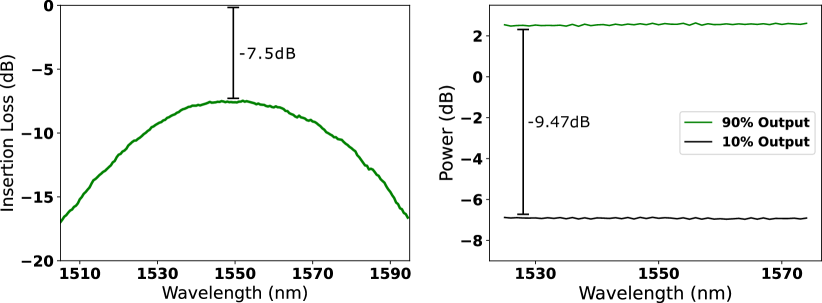
We can start by working out the loss due to our grating couplers, which we can estimate using a short loopback structure, and a 90:10 fibre coupler. The loopback structure consists of two grating couplers, and enough waveguide to physically connect them together. The 90:10 fibre coupler gives us an estimate of the pump power that we are sending to the chip. The characterisation for both of these components is shown in Fig. S9, and tells us that our loss per grating coupler is 3.75 dB (which is what we expect from this standardized component), and our 90:10 fibre coupler is operating as an 89:11 coupler.
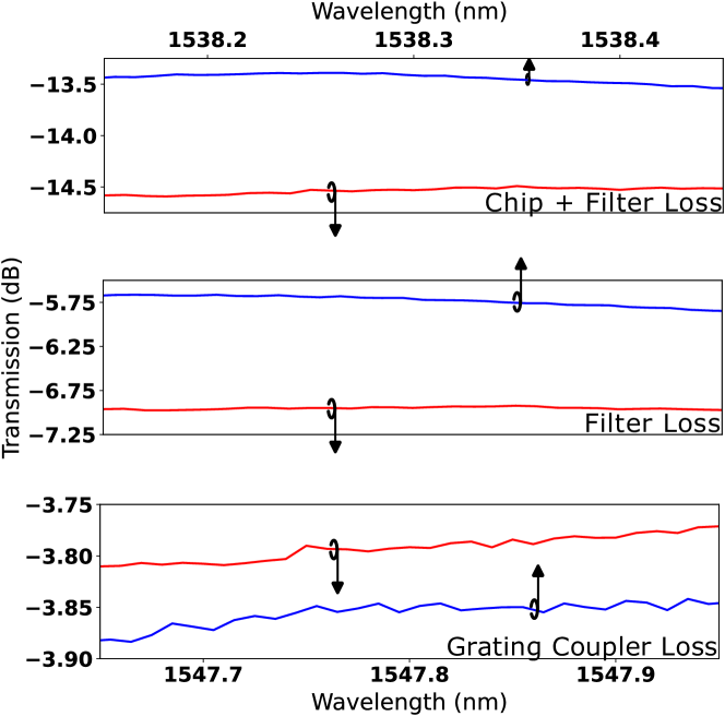
After this preliminary characterization, we move on to the source structure itself. We need to measure the experimental setup in two configurations, once through the chip and the entire filter network, and once with just the filter network. The results of these measurements are presented in Fig. S10. This lets us reconfirm our measurements of the grating coupler loss that we got earlier (Fig. S9), which we can see agree well.
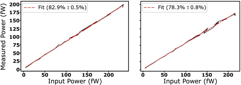
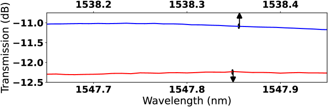
This leaves us with two remaining loss measurements, from the filters to the detector system, and the detection efficiency of the detectors themselves. Using a commercial optical power meter, we measured the transmission loss between the filters, and the detector system to be -0.42 0.02 dB and -0.71 0.02 dB for the signal and idler channels, respectively. As for the detector characterization, this work was done earlier by Laurent Kling and Stefano Paesani who we acknowledged in the main text. The outcomes of these measurements are shown in Fig. S11. Giving us a final loss per channel shown in Fig. S12
Subtracting these losses from the calculated heralding efficiencies, we see source heralding efficiencies of = 92.1 3.2 %, and = 94.0 2.9 % as in the main text.
XII Assumptions in Approximating the JSA as the
Our assumption that we made in the main text comes from the fact that we typically perform intensity measurements of the JSA using SET, rather than phase-sensitive ones. In our case, phase-sensitive measurements are unnecessary because, if we simulate the JSA and the JSA the difference in purity is only 0.01% which is within the error of our experimental data. The difference between these two simulations is simple, in one case the phase of the JSA () is non-zero, and in the case of the JSA it is neglected and assumed to be zero (Fig. S13).
XIII Error Analysis of the Experimental JSI
Analyzing the experimental JSI properly is important to be able to say with certainty that the estimated purity is a good representation of the data. In our case, we did this by making use of the high-resolution of our equipment (0.16 pm, and 1 pm for the idler and signal axis, respectively). By averaging across several pixels in the JSI, we can reduce the error due to experimental noise. Mostly, experimental noise comes from the accuracy of our optical spectrum analyzer (OSA), and the precision to which we can set the wavelength of our very narrow linewidth seed laser. We can see that by the time we are at a resolution of , the purity value of the JSI is plateauing (Fig. S14), and the error is minimized. This means that we can say with certainty that the value we quote for the purity of our photonic molecule, is representative of its real-world value.
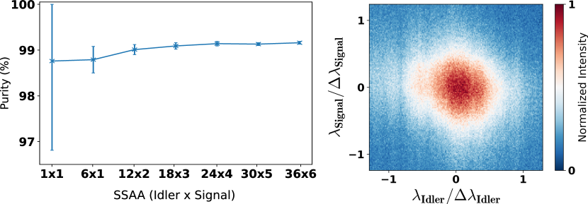
As for how we calculate the error on our JSI, we can take a look at the noise distribution of our high-resolution JSI. We can isolate the uncertainty on each data point of the JSI by measuring the variance of each pixel when compared to its neighbor. This works because the noise varies much quicker than the JSI, on the order of individual data points (looking at the speckle on the JSI in Fig. S14) rather than on the order of thousands of pixels. This gives us an error of 4% on each data point. We can work out how sensitive the JSI is to noise by using Monte Carlo simulations and our estimated error on each pixel. This gives us the error that we use in the main text, and in Fig. S14.