Flat bands and multi-state memory devices from chiral domain wall
superlattices in magnetic Weyl semimetals
Abstract
We propose a novel analog memory device utilizing the gigantic magnetic Weyl semimetal (MWSM) domain wall (DW) magnetoresistance. We predict that the nucleation of domain walls between contacts will strongly modulate the conductance and allow for multiple memory states, which has been long sought-after for use in magnetic random access memories or memristive neuromorphic computing platforms. We motivate this conductance modulation by analyzing the electronic structure of the helically-magnetized MWSM Hamiltonian, and report tunable flat bands in the direction of transport in a helically-magnetized region of the sample for Bloch and Néel-type domain walls via the onset of a local axial Landau level spectrum within the bulk of the superlattice. We show that Bloch devices also provide means for the generation of chirality-polarized currents, which provides a path towards nanoelectronic utilization of chirality as a new degree of freedom in spintronics.
I Introduction
Topological materials such as topological insulators, Dirac semimetals, and Weyl semimetals have gained much interest for their litany of novel electron transport behaviors and potential utility in nanoelectronic devices [1, 2, 3]. Weyl semimetals in particular must break either inversion or time-reversal symmetry (TRS). In a magnetic Weyl semimetal (MWSM), a Dirac cone is split into two Weyl cones with opposite chiralities when TRS is broken, giving rise to effects such as the chiral anomaly or negative longitudinal magnetoresistance (MR) [4, 5].
In intrinsically magnetic Weyl semimetals, the helicity of Weyl fermions can be controlled by changing the magnetization of the material, giving rise to large longitudinal MR via the helicity mismatch of carriers in differently-magnetized portions of a sample. Previous works [6, 7] have looked at this MR associated with transport across MWSM domain walls (DWs) and a magnetic tunnel junction (MTJ) constructed from MWSMs, both of which conclude that on/off ratios could be improved significantly () over the MRs utilized in traditional CoFeB/MgO MTJs. This giant Weyl MR arising from spatially-varying magnetic textures is expected to be resilient to disorder and large when compared to the DW resistances attributed to anisotropic MR or spin-mistracking in a nontopological DW [8, 9]. Such a material platform has been long-sought after in neuromorphic computing or analog memory architectures [10, 11, 12, 13, 14], but the fast write times and energy efficiency of existing spintronic memories have been offset by inefficient readout owing to low MRs in MTJs, often necessitating peripheral CMOS circuitry [15, 16].
Experimentally, an elevated longitudinal MR of was observed by nucleating DWs in a sample of Weyl ferromagnet Co3Sn2S2 [17] at 100 K. Other works [18, 19, 20] predict that the chirality-magnetization locking will cause carriers to localize at discontinuities in the magnetization profile, which along with the recently observed topological hall torque [21, 22], opens up orders-of-magnitude more efficient means for electronic control of magnetic information in MWSMs. Recently, one helitronic magnetic memory platform has been proposed for unconventional computing, for which MWSM DW MRs could massively improve readout efficiencies [23]. Furthermore, the carrier localization and chirality - magnetization locking in MWSMs motivates interest in transport and the electronic structure of the periodic exchange superlattices, with the starting intuition that conductance should be forbidden in the direction of alternating magnetic texture. Previous works [18, 19] have shown that Néel DWs will localize carriers in 1D coplanar to the DW, but a detailed understanding of the connection between periodic magnetic textures, artificial gauge fields, and spinful electronic bandstructures in 3D is lacking.
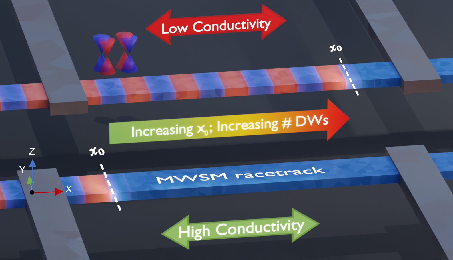
In this work, we propose a novel multi-state MWSM DW memory device (depicted in Fig 1) and investigate the ensuing electronic structure of MWSMs in a helical spin texture. We show that states are subjected to an effective sinusoidal potential in spin space, locally generating axial Landau levels below a certain energy threshold and find a condition for the generation of bulk flat bands. With this intuition, we are able to show that the nucleation of additional domain walls between contacts will modulate the conductance of the whole device, and that this effect persists for even trivial metallic electrodes. Experimentally, such a system could potentially be realized in a MWSM helimagnet or via injection of chiral DWs into a magnetic racetrack [24] with mean-free-path larger than the superlattice length.
II Domain wall superlattices and plane-wave analysis
We consider two models to elucidate the electronic structure and transport in periodically-magnetized MWSM superlattices: one using the continuum plane-wave basis model with a perfectly helical spin texture and another using the standard tight-binding approximation for transport. For both models, we consider the cases of Néel (N) and Bloch (B) magnetic DW lattices with the spatially-variant exchange field defined as
| (1) | ||||
| (2) |
where is a spatially-dependent magnetization angle. For the infinite superlattice along , can be defined as , where the reciprocal lattice length is the superlattice period of unit cells of length . Later, we define for a series of chiral DWs. For the continuum model, we take the four-band model Hamiltonian of a TRS-broken MWSM [1]:
| (3) |
defined in the spin () and pseudospin () spaces, where denotes the Fermi velocity and is a mass-like term. Imposing a 1D superlattice structure in and adding the Fourier-transformed exchange field 111See Supplemental Material at [URL will be inserted by publisher] to the Hamiltonian off-diagonal terms result in
| (4) |
In our model, we take 222. This is used for comparison with the tight-binding model. In real MWSMs, this is roughly an order of magnitude lower [21], but this does not change the underlying physics. and focus on in this paper. An exchange splitting magnitude of is taken to split the Weyl nodes with a small with nm, and for comparison with previous work [6].
For a constant magnetization, the exchange field will split the chiral Weyl points (which we can denote with ) in momentum space as . Then an equivalent low-energy model for the Weyl cone dispersions can be taken as [1, 18, 19, 3]
| (5) |
where leads to a chirality-dependent magnetic field determined by the exchange field texture:
| (6) |
which generates an axial magnetic field
| (7) | |||
| (8) |
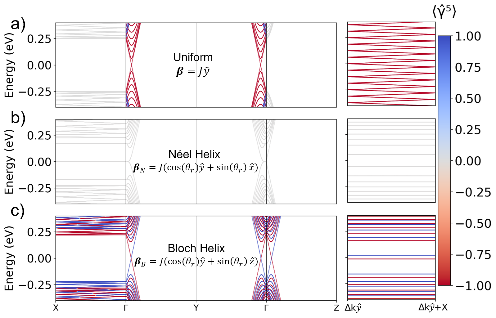
for the Néel and Bloch wall cases, respectively. Applying this axial vector potential field to our system significantly modifies the band structure, generating flat bands and chirality-dependent axial Landau levels (LLs), shown in Fig 2, where we plot the chirality-projected bands for the uniformly magnetized, Néel, and Bloch helical-exchange superlattices. The chirality operator has eigenvalues corresponding to , and is computed with the time-retarded Green’s function in this section. While straightforward to project the Bloch eigenstates as , it would be misleading in the Néel wall case as the and states are degenerate, thus obscuring one or the other. It is most interesting to note the generation of bulk flat bands in the direction of transport and axial LLs above the exchange-split momenta of the Weyl cones, which we will discuss further for each case. Both of these phenomena are explained in the low-energy model by the construction of Bloch functions in terms of localized harmonic oscillators created by the mixture of magnetic exchange and momentum terms.
II.1 Neel Helix Hamiltonian
To understand the Néel Helix Hamiltonian , it is first useful to gauge away the term of , leaving the observables of the Hamiltonian unchanged:
| (9) | |||
| (10) | |||
| (11) |
We may notice is diagonal in spin space. Thus, we can motivate the wavefunctions for each spin .
| (12) | |||
| (13) |
For realistic physical values of , and for small enough , the above expressions reduce to the Mathieu differential equation from the dominant term – notably without general analytic solutions. However, we can note that two locally-parabolic potential wells are created around regions of large , implying charge localization around . Increasing small values of will tilt the potential wells, introducing anharmonicity away from , but ultimately preserving the charge localization for small enough . This is consistent with an intuition of a which may localize charges in x and y. Around , we can locally understand LL generation in by defining the operators
| (14) | |||
| (15) |
which commute as
| (16) |
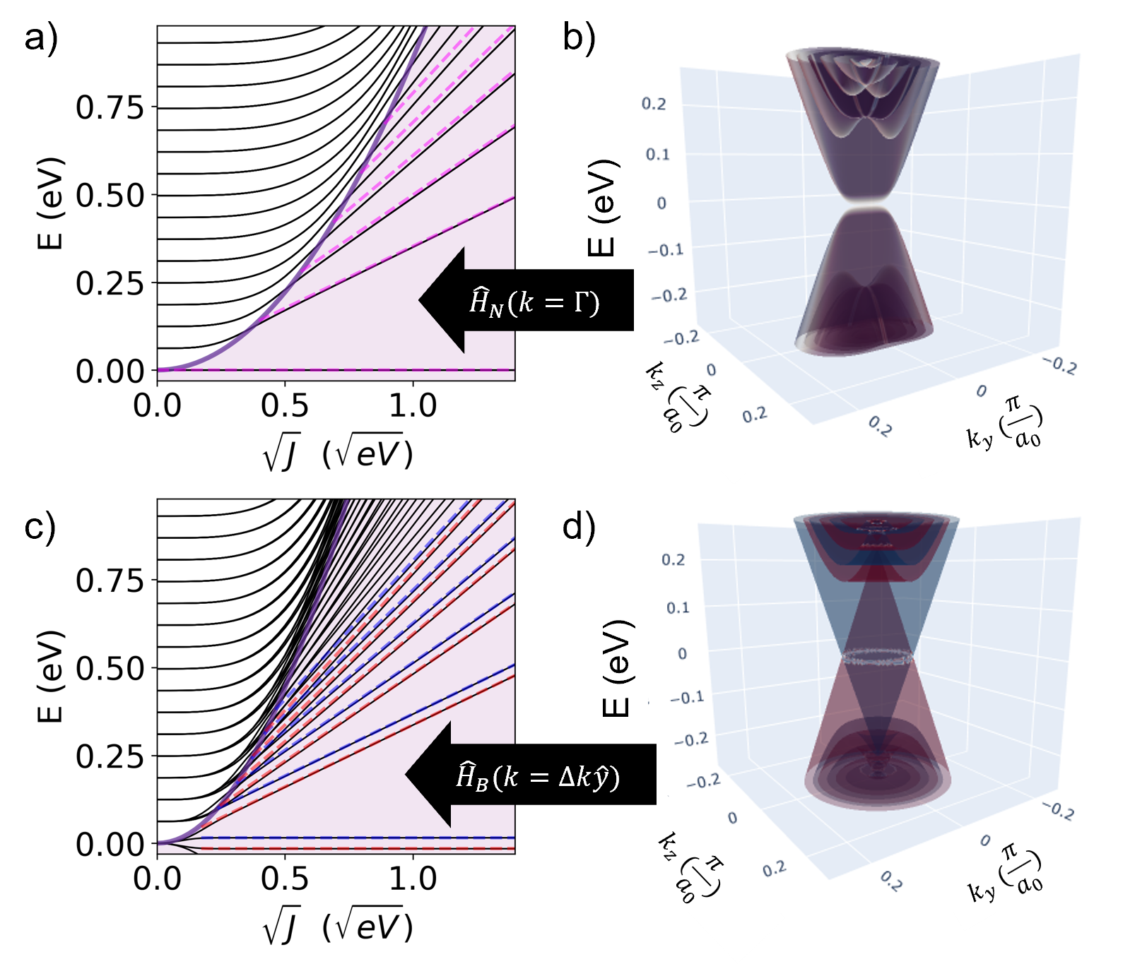
around the localized wavepackets. Thus, and switch roles as the creation and annihilation operators in different regions of the lattice and for differing electron chiralities. Linearizing the exchange term and mapping the problem onto the standard Dirac LL Hamiltonian, is predictive of the energy spacings for small enough n, as shown in Fig. 3 (a):
| (17) | |||
| (18) |
We may take as a guess that the 0th axial LL may have 0 energy at , and proceed to directly solve for the null space of , leaving us with two expressions for the corresponding states.
Finally, with a separation of variables, we can exactly solve for the zero-mode wavefunctions of each spin:
| (19) |
which, around the potential wells, are well approximated by gaussians of characteristic magnetic length
| (20) |
thus acting as a well-defined 0th LL state. This tells us that the local axial LL model may hold in the limit where the local Bloch function spread (as determined by ) is much less than the superlattice length, which will be discussed shortly.
II.2 Bloch Helix Hamiltonian
The prior analysis fails for the Bloch wall case, motivating us to consider other techniques to explain the behavior of . Qualitatively, we expect an analogous axial LL physics should manifest for the Bloch wall case, though the continuously changing direction of makes it somewhat obscure: rotates with constant magnitude in the plane as a function of . As a result, the zeroth Landau level disperses in different directions at well-defined positions in real-space, which can be seen in Fig. 2 (c) for the and directions. We do observe that the magnetization profile (Eq. 2), which decides the separation of two Weyl nodes, leads to a nodal-ring structure in the spectrum in the plane centered at . To analyze this, first we will rotate with oriented in , and translate the magnetic potential term while preserving its spatial helicity. Defining , in cylindrical coordinates, and exploiting Euler’s identity, we can write the transformed Hamiltonian as
| (21) |
We can then change the basis to diagonalize the exchange term and square , giving us some insight on the form of the wavefunctions:
| (22) |
This implies that the Hamiltonian produces a continuum of locally-parabolic potential wells per unique , and that the solutions will take the form of slightly modified Mathieu special functions for , this time with doubled spatial period and a single well per superlattice unit cell. Unfortunately, the off-diagonal term immensely complicates our analysis, mixing the solutions of the diagonal Mathieu () and Mathieu-like () ODES. For further insight into the spin structure and of , we can replace with (for consistency with analysis), define and solve for the components of by substitution (see appendix 333See Supplemental Material at [URL will be inserted by publisher] for full derivation.). This is not analytically tractable in general, but we find two unnormalized solutions at , , and :
| (23) |
We turn to numerics to find the spectrum of the system, and see that, as shown in Fig. 3 (c),
| (24) |
is indeed predictive at . This implies the complex-modulated wavefunctions may indeed act as an exotic twisted 0th LL, however needs more analysis to determine a pair of operators which may obey the harmonic oscillator commutation relations. Interestingly, the dispersion for can be obtained analytically 444See Supplemental Material at [URL will be inserted by publisher] for full derivation and is given by:
| (25) |
so that the lowest-energy -chiral bands are raised and lowered in energy with at the point for a magnetic texture with right-handed spatial helicity and remain dispersive in .
II.3 Localization and band-flattening
Both cases lead to a infinite lattice of locally-parabolic potential wells, which gives us a means to analyse the band flattening by considering a minimal tight-binding model. For a localized LL state,
| (26) |
which provides a heuristic condition for band flattening as a function of axial LL index, supposing individual tightly-bound wavepackets may have negligible overlap. The Bloch and Néel wall cases provide 1 and 2 potential wells per unit cell respectively, thus:
| (27) |
Translating this into an energy cutoff, we expect to see the onset of carrier localization for
| (28) |
for the Néel and Bloch cases. As shown in Fig. 3, this approximation matches well with the calculated spectrum, predicting the onset of well-defined dirac LL energies.
In both cases, we understand that the electronic bands are significantly flattened in the direction of the superlattice by generating an emergent periodic potential for each spin, and provide a heuristic to predict the onset of the bulk flat band state. This shows that the application of spatially-varying or periodic magnetic textures in MWSMs provides a means to disable dispersion by effectively imposing a series of tunneling barriers in spin space, thus providing dynamic control over the electronic structure. With this in mind, we move to a device picture to assess one application of MWSM DW lattices.
III Quantum transport and tight-binding analysis
For transport and spatial resolution of the distorted Weyl cones, we employ a four-band, two Weyl point (see footnote 555It is necessary to include a k-dependent mass term, as explained in [7], in order to create a single pair of Weyl cones near the center of the Brillouin zone at with [6], though is near-zero in the region of the Weyl points) tight-binding model of a MWSM [6], though instead choose the and matrices for the momentum and mass terms, as in Eq. 4:
| (29) |
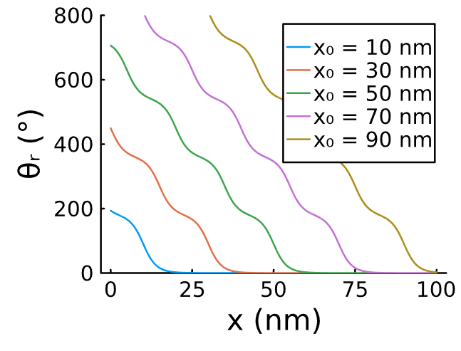
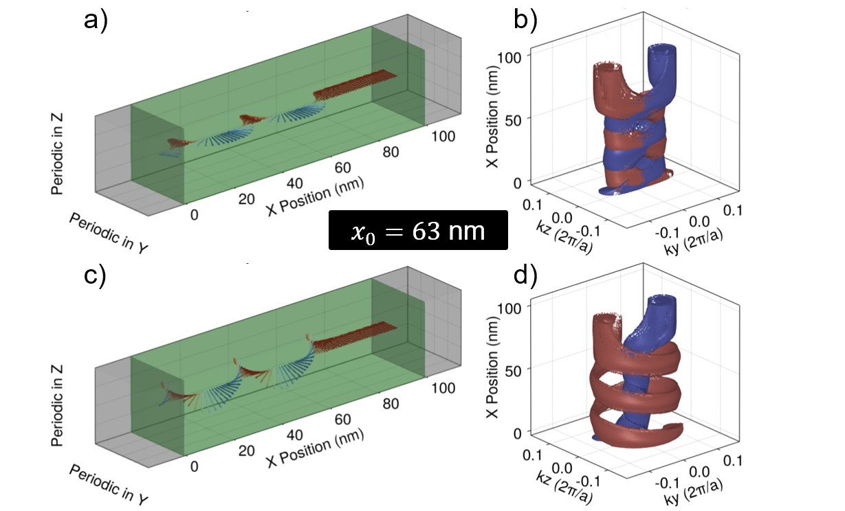
with hopping parameter 1 eV, lattice parameter 1 nm for simplicity, 100 total sites in x, and the Bloch phase prefactors applied to hoppings in and to construct a supercell . Here, of a DW is defined in [31] and convolved with a semi-infinite Dirac comb to generate the magnetization angle (see Supp. Fig. 7):
| (30) |
with being the convolution operator, referring to the start position of the chiral DW lattice, the DW width nm, and a truncated superlattice period nm. While these parameters are not necessarily physical with relevance to the modelling of real magnetic racetrack systems, they are a minimal model that is computationally tractable and allows us to demonstrate underlying physics. In a real system, thicker domain walls or a longer would decrease max() [19] thus decreasing the axial LL spacing and zone-folded subband spacing.
In the tight-binding model, we consider trivial metallic electrodes 666We take a simple, spin and orbital-degenerate toy metal Hamiltonian with an arbitrary eV and eV and semi-infinite MWSM electrodes to elucidate the underlying physics. For the case with MWSM electrodes, the magnetizations are copied for the left and right contact and extend to infinity for the generation of the Sancho-Rubio [34] contact self-energies to retain the continuity of the magnetization field texture.
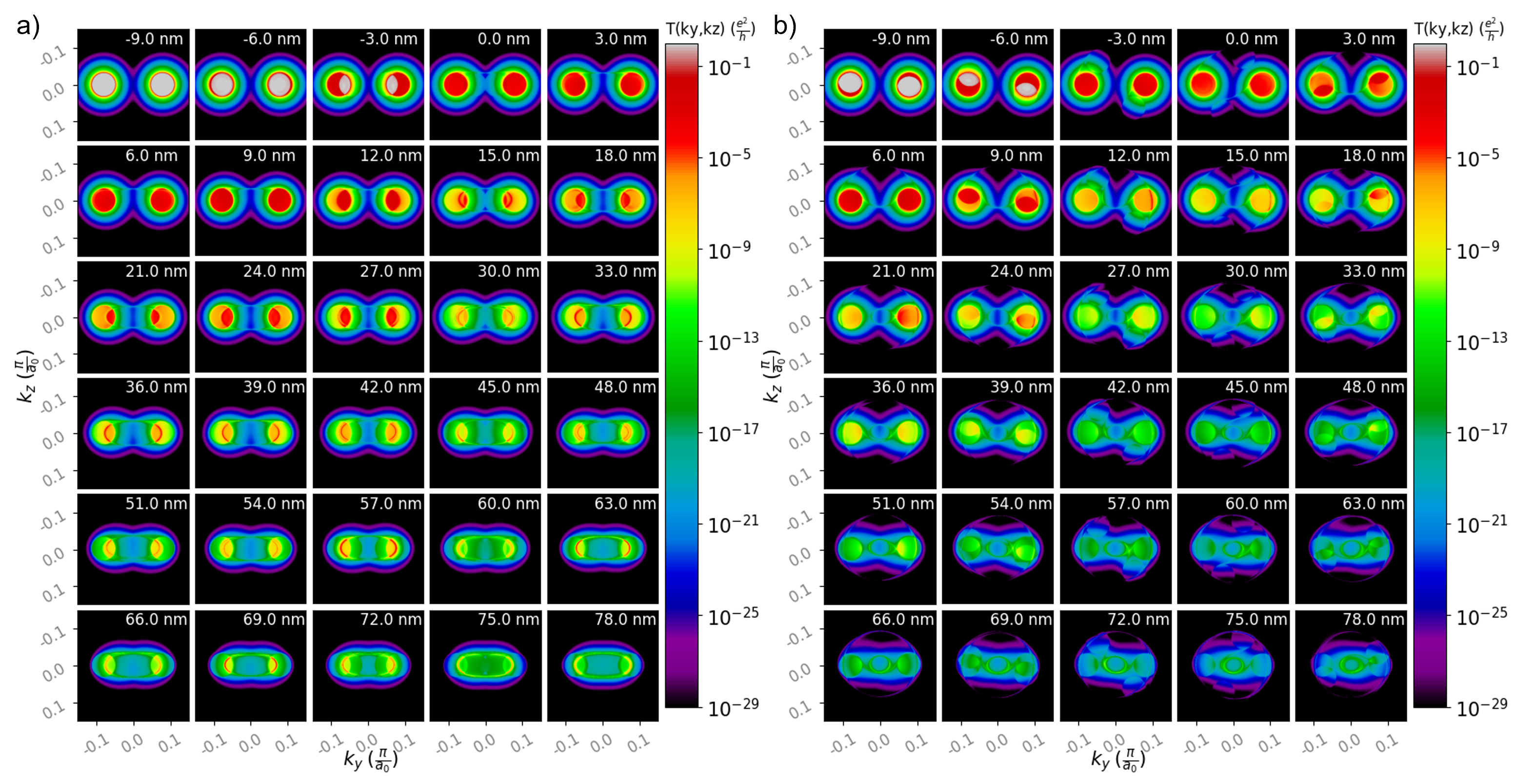
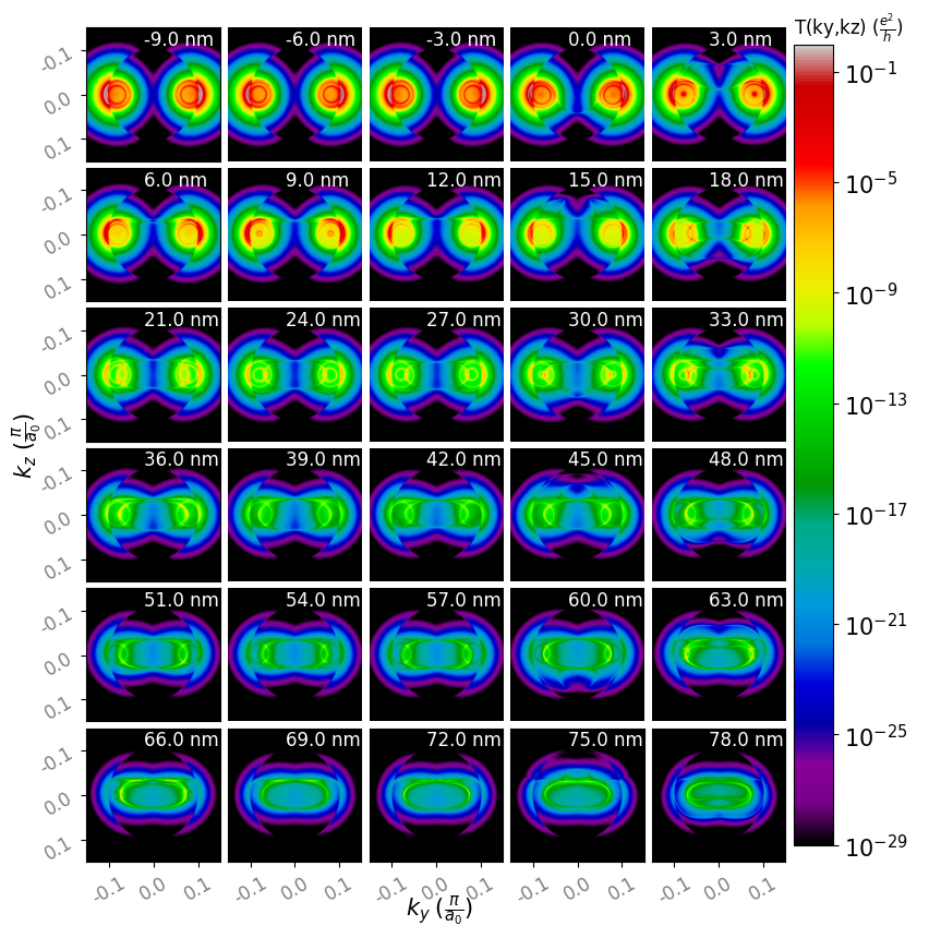
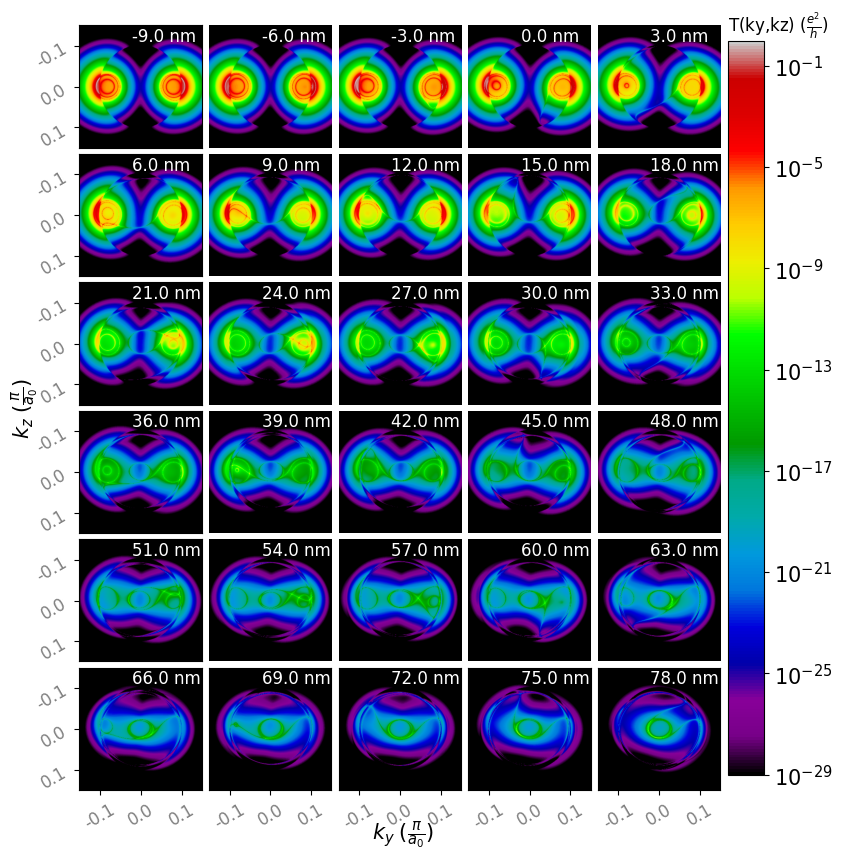
Of particular interest is the distortion of the Weyl cones in connection with the band structures of Fig. 2, which are useful to understand transport. For all transport calculations and tight-binding modelling, we take a chemical potential eV to cut through the 0th axial LL from Sec. II, and note that henceforth refers to the lifetime broadening. Fig. 4 plots isosurfaces of the chirality, position, and -resolved local density of states (LDOS) of the periodically magnetized racetrack devices, allowing us to spatially resolve the distorted Weyl cones which construct the bulk harmonic oscillator states. Néel devices show a -symmetric twisting of the and Weyl cones, corresponding to the degenerate states in Fig. 4 (b). This can be understood from the profile of for the Néel case which decides the position of two Weyl nodes in the plane. On the other hand, for the Bloch DW case, rotates in , twisting the Weyl cones as shown in Fig. 4 (d) where for an infinitesimal non-zero energy, and states are at a different radius in the plane. We see the chiral states wrap around the expected position of the Weyl points at , while the chiral states wrap closely to for our chosen , having been lifted up in energy from Eq. 25. These twisted Weyl cones motivate analysis of the chiral anomaly and Weyl orbits with periodic real and axial magnetic fields (see recent insights in [35]).
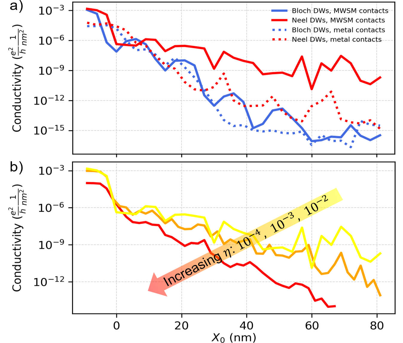
For device modeling, we neglect the orbital effects of the magnetic field and consider transport in the Landauer limit of the NEGF quantum transport formalism 777See [48]; . With a minimal carrier lifetime broadening of eV, in Fig. 5 (a) we show that device conductance can be modulated by orders of magnitude via the injection of DWs into the active region of the device, and that this effect persists for both magnetization patterns, with both MWSM and simple metal electrodes. In Fig. 5 (b), for a system with MWSM electrodes we sweep the broadening parameter , corresponding to a phenomenological inelastic momentum-preserving scattering self-energy [37], and show that it 1) smooths out conductivity vs. and 2) forms stairsteps in conductance with respect to the number of DWs in the active region of the device–as one might expect with an increasing number of spin-dependent tunneling barriers. A similar behavior is observed for the Bloch wall case.
Curiously, even a high-resolution 401 x 401 k-grid over the zoomed-in portion of the surface Brillouin zone (SBZ) is unable to converge the value of the Landauer conductance for small broadening parameters ( eV), leading to unphysical spikes in conduction. To explain this, we consider the -resolved transmission with MWSM electrodes in Fig. 6 (a) and Fig. 6 (b) to resolve conductance behavior from the distorted Weyl cones in the periodic magnetization region. We see that the distorted Weyl cones in the bulk form infinitesimally-thick curtains of conductance in the SBZ which are challenging to capture numerically: In Fig. 6 (a), the Néel DW lattice conduction is dominated by the distorted and Weyl cones in the periodic region of the device, especially where they overlap with the contact electrodes’ bulk Weyl cones. In contrast, the Bloch DW device in Fig. 6 (b) has minimal conduction through the distorted Weyl cones which wrap around the bulk Weyl cone states from either contact. Thus, the majority of the conductance tunnels through the periodic region of the device from the Bulk states in both contacts, leading to oscillations in Fig. 5 (a). The case with metal contacts in Fig. 5 (a) is somewhat more convoluted, given the formation of surface Fermi arcs at the metal/MWSM interface, though the properties of the device Hamiltonian and bulk Fermi arcs still dominate the qualitative behavior when sweeping . Metal-contact -resolved transmission plots are provided in the supplementary for both Néel and Bloch cases. Interestingly, due to the broadening parameter providing finite-lifetime states from both the MWSM and metal contacts, in our magnetization with left-handed spatial chirality, transport from the inner -chiral transmission ring will begin to dominate the total conductance, giving rise to a texture-dependent chirality filtering mechanism to generate or reflect chiral currents. In principle this would be tunable with a modulation in fermi level or magnetic texture, opening another means for generating chiral currents with potential in emerging devices [38].
IV Discussion
We have explained the electronic structure and transport in a MWSM superlattice device, have shown magnetization-tunable axial LLs and flat bands in the direction of transport, and have demonstrated that multiple conductance states could potentially be encoded in such a device. We have also shown that the multi-state conduction behavior persists through all electrode configurations we have considered, unlike the spin transport in traditional spin filtering systems. With regards to the superlattice picture, the exploration of periodic exchange textures or artificial gauge fields and their topological structure is nascent in systems such as semiconductor nanowires [39], magnetic superlattice graphene [40], or 2D Moiré magnets [41]. It should be noted that this effect only relies on the mean-field exchange splitting of a periodic ferromagnet, acting on spin space with contributions on the order of 100 to 1000 meV in bulk ferromagnets, as opposed to a real magnetic field or proximity-induced exchange, the effects of which would show with much weaker contribution to an effective gauge field. Thus, we expect the electronic structure in periodic MWSM lattices to be more robust closer to room temperatures, supposing a MWSM with Curie temperature above 300 K as in Mn3Sn[42], Co2MnGa[43], or Fe3Sn2[44]. Nevertheless, other perspectives on scattering at MWSM DWs imply that skew scattering [45] or heavily-tilted Weyl cones [46] could significantly decrease the MR.
This highly-tunable electronic structure and conductivity via control of magnetization in MWSMs would be of great use to nanoelectronics, which we will discuss briefly. Even with additional achiral bands at the Fermi energy, non-magnetic electrodes, or a modest carrier relaxation length just greater than the width of the DW, a meager DW MR could be improved by chaining DWs along the length of the device to 1) improve the overall on/off ratio and 2) encode multiple bits of information in a single memory device. While it is hard to make definitive claims from our model without incoherent momentum relaxation – we see longitudinal Weyl MRs over – we estimate that, using the DW resistances observed in [17] an effective MR could be achievable for the observed and for a domain width nm and device length nm. This is 14x the 3.93% read margin observed in CoFeB transverse-read DW memory [9]. In itself, this becomes competitive with other GMR devices (with regards to on/off ratio) or multi-state TMR devices [47], but without the need of a magnetic tunnel junction to measure the magnetization-induced resistance change. Supposing a deliberate engineering of the chemical potential or DW width could bring about a modest DW MR with m, and nm, on/off ratios upwards of 650% become possible. Another potential advantage of this approach, compared to traditional DW-MTJ devices, is that one could avoid the need for precise MgO deposition to avoid pinholes, thus making high MRs accessible to industry and academic labs without lengthy and expensive fabrication processes. Here, one could construct memory devices using simple metallic thin films, so long as the chirality-magnetization locking in the MWSM is preserved and surface fermi arcs do not dominate the conductance. Predicted orders-of-magnitude-improved readout performance over existing MTJs [6] could further increase device viability, supposing one could amplify the Weyl MR or suppress scattering in a real system.
Note added: Recently, we became aware of a paper which considers the Bloch helix case and describes this system as a ’Fermi Arc Metal’, reporting further on the conductance in real magnetic fields [35].
V Acknowledgements
The authors acknowledge funding from the UT CDCM MRSEC supported under NSF Award Number DMR-1720595, funding from Sandia National Laboratories, and computational resources from the Texas Advanced Computing Center (TACC) at the University of Texas at Austin. The authors also greatly thank Eslam Khalaf and Gregory A. Fiete for helpful insights, as well as Kerem Camsari and Shuvro Chowdhury for their discussions on the theory and implementation of the NEGF transport formalism.
References
- Armitage et al. [2018] N. Armitage, E. Mele, and A. Vishwanath, Reviews of Modern Physics 90, 015001 (2018).
- Burkov [2018] A. Burkov, Annual Review of Condensed Matter Physics 9, 359 (2018).
- Ilan et al. [2020] R. Ilan, A. G. Grushin, and D. I. Pikulin, Nature Reviews Physics 2, 29 (2020).
- Hu et al. [2019] J. Hu, S.-Y. Xu, N. Ni, and Z. Mao, Annual Review of Materials Research 49, 207 (2019).
- Nagaosa et al. [2020] N. Nagaosa, T. Morimoto, and Y. Tokura, Nature Reviews Materials 5, 621 (2020).
- de Sousa et al. [2021] D. J. P. de Sousa, C. O. Ascencio, P. M. Haney, J. P. Wang, and T. Low, Phys. Rev. B 104, L041401 (2021).
- Kobayashi et al. [2018] K. Kobayashi, Y. Ominato, and K. Nomura, Journal of the Physical Society of Japan 87, 073707 (2018).
- Kent et al. [2001] A. D. Kent, J. Yu, U. Rüdiger, and S. S. P. Parkin, Journal of Physics: Condensed Matter 13, R461 (2001).
- Roxy et al. [2020] K. Roxy, S. Ollivier, A. Hoque, S. Longofono, A. K. Jones, and S. Bhanja, IEEE Transactions on Nanotechnology 19, 648 (2020).
- Chen et al. [2021] J. Chen, J. Li, Y. Li, and X. Miao, Journal of Semiconductors 42, 013104 (2021).
- Li et al. [2018] Y. Li, Z. Wang, R. Midya, Q. Xia, and J. J. Yang, Journal of Physics D: Applied Physics 51, 503002 (2018).
- Wan et al. [2022] W. Wan, R. Kubendran, C. Schaefer, S. B. Eryilmaz, W. Zhang, D. Wu, S. Deiss, P. Raina, H. Qian, B. Gao, S. Joshi, H. Wu, H.-S. P. Wong, and G. Cauwenberghs, Nature 608, 504 (2022).
- Wang et al. [2022a] C. Wang, Z. Si, X. Jiang, A. Malik, Y. Pan, S. Stathopoulos, A. Serb, S. Wang, T. Prodromakis, and C. Papavassiliou, IEEE Journal on Emerging and Selected Topics in Circuits and Systems 12, 723 (2022a).
- Zarcone et al. [2020] R. V. Zarcone, J. H. Engel, S. Burc Eryilmaz, W. Wan, S. Kim, M. BrightSky, C. Lam, H.-L. Lung, B. A. Olshausen, and H.-S. Philip Wong, Scientific Reports 10, 6831 (2020).
- Jung et al. [2022] S. Jung, H. Lee, S. Myung, H. Kim, S. K. Yoon, S.-W. Kwon, Y. Ju, M. Kim, W. Yi, S. Han, B. Kwon, B. Seo, K. Lee, G.-H. Koh, K. Lee, Y. Song, C. Choi, D. Ham, and S. J. Kim, Nature 601, 211 (2022).
- Brigner et al. [2022] W. H. Brigner, N. Hassan, X. Hu, C. H. Bennett, F. Garcia-Sanchez, M. J. Marinella, J. A. C. Incorvia, and J. S. Friedman, in 2022 IEEE International Symposium on Circuits and Systems (ISCAS) (2022) pp. 1189–1193.
- Shiogai et al. [2022] J. Shiogai, J. Ikeda, K. Fujiwara, T. Seki, K. Takanashi, and A. Tsukazaki, Phys. Rev. Mater. 6, 114203 (2022).
- Araki et al. [2018] Y. Araki, A. Yoshida, and K. Nomura, Physical Review B 98, 045302 (2018).
- Grushin et al. [2016] A. G. Grushin, J. W. F. Venderbos, A. Vishwanath, and R. Ilan, Phys. Rev. X 6, 041046 (2016).
- Kurebayashi and Nomura [2019] D. Kurebayashi and K. Nomura, Scientific Reports 9, 5365 (2019).
- Yamanouchi et al. [2022] M. Yamanouchi, Y. Araki, T. Sakai, T. Uemura, H. Ohta, and J. Ieda, Science Advances 8, eabl6192 (2022).
- Wang et al. [2022b] Q. Wang, Y. Zeng, K. Yuan, Q. Zeng, P. Gu, X. Xu, H. Wang, Z. Han, K. Nomura, W. Wang, E. Liu, Y. Hou, and Y. Ye, Nature Electronics , 1 (2022b).
- [23] N. T. Bechler and J. Masell, Neuromorphic Computing and Engineering 3, 034003.
- Filippou et al. [2018] P. C. Filippou, J. Jeong, Y. Ferrante, S.-H. Yang, T. Topuria, M. G. Samant, and S. S. P. Parkin, Nature Communications 9, 4653 (2018).
- Note [1] See Supplemental Material at [URL will be inserted by publisher].
- Note [2] . This is used for comparison with the tight-binding model. In real MWSMs, this is roughly an order of magnitude lower [21], but this does not change the underlying physics.
- Note [3] See Supplemental Material at [URL will be inserted by publisher] for full derivation.
- Note [4] See Supplemental Material at [URL will be inserted by publisher] for full derivation.
- Araki and Nomura [2018] Y. Araki and K. Nomura, Phys. Rev. Appl. 10, 014007 (2018).
- Note [5] It is necessary to include a k-dependent mass term in order to create a single pair of Weyl cones in the tight-binding model, though is near-zero in the region of the Weyl points.
- O’Handley [1999] R. O’Handley, Modern Magnetic Materials: Principles and Applications (Wiley, 1999).
- Note [6] We take a simple, spin and orbital-degenerate toy metal Hamiltonian with an arbitrary eV and eV.
- Note [7] The semi-infinite MWSM electrodes are useful in the large scattering limit, where an electron will locally see an infinite lattice in all directions. They are also most useful for resolving the Fermi-surfaces, where surface states will confound the fermi surface twisting.
- Sancho et al. [1985] M. P. L. Sancho, J. M. L. Sancho, J. M. L. Sancho, and J. Rubio, Journal of Physics F: Metal Physics 15, 851 (1985).
- [35] M. Breitkreiz and P. W. Brouwer, Physical Review Letters 130, 196602.
- Note [8] See [48]; .
- Philip et al. [2017] T. M. Philip, M. R. Hirsbrunner, M. J. Park, and M. J. Gilbert, IEEE Electron Device Letters 38, 138 (2017).
- Kharzeev and Yee [2013] D. E. Kharzeev and H.-U. Yee, Phys. Rev. B 88, 115119 (2013).
- Kammhuber et al. [2017] J. Kammhuber, M. C. Cassidy, F. Pei, M. P. Nowak, A. Vuik, O. Guel, D. Car, S. R. Plissard, E. P. a. M. Bakkers, M. Wimmer, and L. P. Kouwenhoven, Nature Communications 8, 478 (2017).
- Wolf et al. [2021] T. M. Wolf, O. Zilberberg, G. Blatter, and J. L. Lado, Physical Review Letters 126, 056803 (2021).
- Paul et al. [2023] N. Paul, Y. Zhang, and L. Fu, Science Advances 9, eabn1401 (2023).
- Muduli et al. [2019] P. K. Muduli, T. Higo, T. Nishikawa, D. Qu, H. Isshiki, K. Kondou, D. Nishio-Hamane, S. Nakatsuji, and Y. Otani, Physical Review B 99, 184425 (2019).
- Saito and Nishio-Hamane [2021] T. Saito and D. Nishio-Hamane, Physica B: Condensed Matter 603, 412761 (2021).
- Yao et al. [2018] M. Yao, H. Lee, N. Xu, Y. Wang, J. Ma, O. V. Yazyev, Y. Xiong, M. Shi, G. Aeppli, and Y. Soh, (2018), 1810.01514 [cond-mat] .
- Sorn and Paramekanti [2021] S. Sorn and A. Paramekanti, Physical Review B 103, 104413 (2021).
- Xuan Mei et al. [2021] X. Xuan Mei, M. Chen, and H. Li, Journal of Applied Physics 130, 203901 (2021).
- Leonard et al. [2022] T. Leonard, S. Liu, M. Alamdar, H. Jin, C. Cui, O. G. Akinola, L. Xue, T. P. Xiao, J. S. Friedman, M. J. Marinella, C. H. Bennett, and J. A. C. Incorvia, Advanced Electronic Materials , 2200563 (2022).
- Camsari et al. [2023] K. Y. Camsari, S. Chowdhury, and S. Datta, in Springer Handbook of Semiconductor Devices, Springer Handbooks, edited by M. Rudan, R. Brunetti, and S. Reggiani (Springer International Publishing, Cham, 2023) pp. 1583–1599.
Appendix A Supplementary information
A.1 Bloch wall hamiltonian spectrum with
First, one can choose the equivalent block-diagonal matrix for the momentum term in Eq. 4 and set m = 0. This decouples the left (-) and right (+) helical states , and allows one to express the Hamiltonian of the infinitely-periodic hamiltonian with helical exchange field as follows. Let , and let be the superlattice reciprocal vector. We use the definition for in section II:
| (31) | |||
| (32) |
In Fourier space, this can be written as:
| (33) | |||
| (34) |
We will now focus on the Bloch wall case.
| (35) |
Then, the basis transformation corresponding to a rotation about can be used to transform the spin matrices:
and, knowing that , the Hamiltonian can be rewritten as:
| (36) |
| (37) |
| (38) |
with the spectrum of (thus, a diagonal subblock of given as:
| (39) |
A.2 Decomposing Bloch exchange helix Hamiltonian
First, it is useful to rotate the problem with in while preserving the Bloch magnetization ’s helicity:
| (40) |
Introducing and absorbing into , we can rewrite the Hamiltonian for one chirality :
| (41) |
We can then Fourier transform the Hamiltonian in x and y, and change the basis of so as to diagonalize the helical exchange term:
| (42) | |||
| (43) | |||
| (44) | |||
Switching to cylindrical coordinates in x and y, we can define and . We can also rewrite the above expressions:
| (46) |
We can notice that permits a continuous set of spatially translated solutions for each value of . Here, we will also stop and note the correspondence with A.1 for . We may also notice that a corresponding to the position of the uniformly-magnetized -chiral weyl node,
| (47) |
will cancel the spatially constant terms of using a taylor series around in z:
| (48) |
Giving us the insight that the Hamiltonian is locally akin to the Dirac Hamiltonian with an additional off-diagonal term which, if the wavefunctions are represented in a hermite-gauss function basis, will generate states. Squaring and again changing the basis (, ) allows us to decouple the spatially-varying terms of the Hamiltonian for each spin, giving us some insight as explained in the main text:
| (49) | |||
| (50) |
We are unable to solve this exactly, but changing , can manipulate the spin terms of to generate constraints on the wavefunctions, defining .
| (51) | |||
| (52) | |||
| (53) | |||
| (54) |
Composing Eq. 52 and Eq. 54 at and , we can use the Wolfram Mathematica software to find two solutions for a with normalization coefficients :
| (55) |
A.3 Tight-binding transport supplementary figures