Scaling NbTiN-based ac-powered Josephson digital to 400M devices/cm2
Abstract
We describe a fabrication stackup for digital logic with 16 superconducting NbTiN layers, self-shunted -silicon barrier Josephson Junctions (JJs), and low loss, high- tunable hafnium–zirconium oxide (HZO) capacitors. The stack enables 400 MJJ/cm2 device density, efficient routing, and AC power distribution on a resonant network. The materials scale beyond 28 nm lithography and are compatible with standard high-temperature CMOS processes. We report initial results for two-metal layer NbTiN wires with 50 nm critical dimension. A semi-damascene wire-and-via process module using 193i lithography and 50 nm critical dimension has shown cross-section uniformity of across the 300 mm wafer, critical temperature of 12.5 K, and critical current of 0.1 mA at 4.2 K. We also present a design of the resonant AC power network enabled by NbTiN wires and HZO MIM capacitors. The design matches the device density and provides a 30 GHz clock with estimated efficiency of up to 90%. Finally, magnetic imaging of patterned NbTiN ground planes shows low intrinsic defectivity and consistent trapping of vortices in 0.5 m holes spaced on a 2020 m2 grid.
I Introduction
Unsustainable demand for compute power and unsustainable production hardware cost Strubell, Ganesh, and McCallum (2020); Li et al. (2020) open the door to new technology in the post-Moore era. Superconducting digital logic has the potential to provide a sustainable solution for large-scale compute applications positioned between mature CMOS and long-horizon quantum computing. The differentiators for superconducting digital are energy efficiency, high computational density, and high interconnect bandwidth. These features uniquely enable real-time AI training models and greater inclusiveness by distributing to edge systems compute power that currently must be deployed in a centralized data center. Development of a superconducting ecosystem would enable this market and would also enable tactical applications in communications Ilderem (2020) and signal processing Ayala et al. (2021), and would lead to further innovations in areas ranging from quantum computing McDermott et al. (2018) to reversible logic Wustmann and Osborn (2020) and neuromorphic computing Kuncic and Nakayama (2021).
While superconducting integrated circuits have existed for decades at a certain modest device count, success in scaling further has met with challenges. Three major limitations include feature size and layer count in the fabrication process, power distribution to current-bias the Josephson junctions, and superconducting flux trapping failures. In this paper we report progress in all of these areas, centered around a fabrication stack with the required features enabled by an updated materials set.
All state-of-art superconducting fabrication processes for digital circuits are Nb-based Yohannes et al. (2005); Berkley et al. (2010); Tolpygo et al. (2014a); Egan, Brownfield, and Herr (2022). As an elemental superconductor, Nb has a relatively high critical temperature of 9.2 K and can be fabricated using conventional DC sputtering and etch. However, processes scaled to an increased number of metal layers and feature sizes down to 0.25 m have run into fundamental limitations. Problems include 1) unstable material properties caused by a low diffusion constant and complex oxidation, affecting tolerances at sub-micron dimensions Herr ; Pinto et al. (2018); Gupta et al. (2016); Gubin et al. (2005); Tolpygo et al. (2021) 2) low inductance per unit length Tolpygo et al. (2014b); Tolpygo and Semenov (2020) limiting routing density and signal integrity, 3) microwave losses due to inherent materials properties and an easily contaminated surface Yogi and Mercereau (1981), and 4) a low processing temperature requirement Crauste et al. (2013). Nb exhibits degradation of the superconducting properties top-to-bottom through the stack due to the cumulative effects of fabrication processing Verjauw et al. (2021). Wire critical temperature distributions vary widely from process-to-process and from wafer-to-wafer. Further degradation due to hydrogen poisoning is reported Amparo and Tolpygo (2010). The low processing temperature is incompatible with standard industry dielectric process Lindemann, Radecker, and Sperlich (2007), with the overall effect limiting feature size, layer count, and process control.
Fabrication of Nb/AlOx/Nb Josephson Junctions (JJs) is accessible to both academia and industry labs, but these junctions are at the limit of scalability as 1) the barrier is too thin to scale to higher critical current densities without degradation of junction quality resulting in increased losses and spreads Tolpygo et al. (2017), 2) the capacitance of the barrier limits device speed Likharev (1985), and 3) the low thermal budget of 150-200∘ C Migacz and Huber (2003) compromises subsequent fabrication processing of the backend. Integration density has not exceeded 1 MJJ/cm2 with only four layers of metal Semenov, Polyakov, and Tolpygo (2017), and has not exceeded 100 kJJ/cm2 with eight layers Herr et al. (2015). Published approaches for further increase in integration density are based on “self-shunted” junctions with lossy barriers. Lossy barriers compromise circuit performance by increasing fabrication spread in the case of high-Jc ultra-thin barrier AlOx junctions Tolpygo (2016), or by reducing speed in the case of Nb-doped Si junctions Olaya et al. (2010); Gudkov, Kupriyanov et al. (2012).
Current fabrication technology does not support efficient implementation of AC power distribution. An industry shift from DC power to resonant AC was a major advance for energy efficiency, scalability, timing, and gate-delay of superconducting digital circuits Farrell et al. ; Vesely ; Egan et al. (2022); Semenov, Polyakov, and Tolpygo (2017); Ayala et al. (2020). However, the most advanced AC resonator networks are limited in density and power-efficiency due to the lack of critical fabrication features. The geometric transformer used at every bias tap limits integration scale to about 4 MJJs/cm2. Further miniaturization of the transformer increases the input power and on-chip dissipation. Proposals for capacitive coupling Strong et al. (2020); Herr, Herr, and Strong (2020) would enable higher integration scale but requires small, high- MIM capacitors. Static power dissipation in the resonator may dominate the total power budget, arising from losses in the Nb wires and dielectrics. AC power distribution across multiple chips is constrained by a lack of tunability of the high-Q resonant power network, needed to compensate for fabrication-induced resonance frequency spreads.
The largest SFQ circuits have been powered by low-speed meander lines Herr et al. (2015); Semenov, Polyakov, and Tolpygo (2017), but meander lines at GHz frequencies have shown limitations due to reflections of the traveling waves in the package, speed-of-light uncertainty on-chip, and power dissipation Herr et al. (2013). A meander-line 4-bit AQFP CPU was demonstrated at 100 kHz, and subcomponents at 2.5 GHz. A resonant clock network based on standing waves was first put forward in the context of QFPs Hosoya et al. (1991) and was finally demonstrated in RQL Strong et al. (2022), with small circuits operating at 10 GHz and circuits of 40,000 JJs at 3 GHz. Further scaling was limited by the large physical size of the transformer in each bias tap. Scaling of superconductor ICs requires fundamental changes to move beyond all of these limitations.
II Fabrication Stack
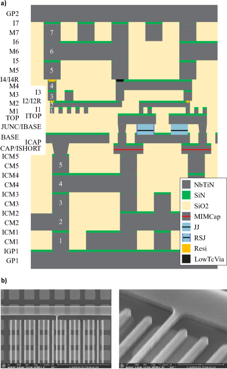
We propose three process modules: NbTiN high-kinetic-inductance wires, Nb/Si/Nb Josephson junctions with self-aligned shunts, and tunable HZO MIM capacitors. All of these materials have been explored and developed in other contexts, but have not been applied to digital integrated circuits. Fig. 1 shows our proposqed fabrication stack with 16 metal layers and two ground planes dedicated to flux-trapping mitigation. Current development is at the level of two metal layers. The stack has balanced resources supporting an integration of 400 MJJs/cm2 matched to HZO-capacitor bias taps, 6 NbTiN backend routing layers with resistors implemented as vias, and 4 NbTiN layers for resonant power distribution. The high kinetic inductance of the wiring supports the high density of junctions and bias taps. In a companion paper Herr, Josephsen, and Herr (ress), we present circuit designs and projected performance of logic and memory mapped onto the fabrication stack.
The frontend of the stack is based on -Si barrier junctions with high quality factor, small capacitance, and integrated shunts. Such junctions meet circuit performance and density requirements: high critical current, high quality, low capacitance, high reproducibility, and tolerance of high temperature processing. These junctions were introduced decades ago Kroger, Potter, and Jillie (1979),Kroger et al. (1985) with impressive characteristics and have recently come back into use Baek, Dresselhaus, and Benz (2006). Relative to Nb/AlOx/Nb, Si-based junctions have 10 the critical current density at 4 thicker barrier. Critical current density of 100 A/m2 produces a 35 A minimum junctions with a diameter of 0.21 m. The small capacitance of these junctions enables them to reach the fundamental switching speed of 1.1 ps based on a gap of 1.8 mV, resulting in 3 reduced gate latency. At the 193i lithography node the total area of each junction instance is less than 0.25 m2 including the via to the base electrode and integrated shunts. A resistive passivation with can act as a self-aligned donut shunt resistor.
The backend process is based on NbTiN wires recently introduced by the quantum and RF superconducting communities driven by the need for small dimensions and extremely low losses Shan, Sekimoto, and Noguchi (2016); Valente-Feliciano et al. (2015); Mazin (2020); Hähnle et al. (2021). Stable and controllable material parameters are a fundamental advantage of this choice. Relative to Nb, NbTiN has up to a 1.8 higher critical temperature at 17.3 K, and a 1.8 higher gap voltage at 5.2 mV. Ti is a nitrogen getter, so higher Ti composition produces a lower number of vacancies and high stability, with processing temperatures up to 1,000 C Valente-Feliciano et al. (2015); Hähnle et al. (2021); Valente-Feliciano et al. (2020); Shu et al. (2021). NbTiN interconnects have extremely low microwave surface resistance Swails (2018); Cyberey et al. (2019) that translates into a 10 higher throughput and 10 less energy per bit compared to Nb. Reported NbTiN wires exhibit stable superconducting properties down to a 1010 nm2 cross section with a critical temperature up to 15 K and a critical current density of 140-200 mA/m2 (see Swails (2018) and references thereof). NbTiN has a 4 lower resistivity translating into a 2 higher critical current than NbN Clem and Kogan (2012).
The high kinetic inductance of NbTiN enables physically small, fixed-inductance-target interconnect without meanders, and upholds signal integrity at deep-submicron by minimizing parasitic mutual inductance arising from the geometric inductance. Target inductance values have low sensitivity to the placement of ground planes and interlayer dielectric (ILD) thickness. A central feature is the ability to design routes to fixed-inductance targets through utilization of layers with different cross-sections that produce a 10 spread in inductance per unit length. Three pairs of routing layers, labeled M1-M6 in Fig. 1, with fine features (50 nm) on the bottom of the stack and coarse features (200 nm) on top, are modeled after CMOS. This methodology would be suitable for inductive and PTL routes using commercial place and route algorithms.
Fabrication of high-kinetic-inductance NbTiN wires requires tight control on wire cross-section that is consistent with 193i lithography and 300 mm wafers. Recent progress on a NbTiN backend process reported by imec Pokhrel et al. (ress) shows 50 nm critical-dimension (CD) wires with cross-wafer CD one-sigma of 1%. The process follows imec’s advances in semi-damascene Ru with 12 nm CD for advanced-node CMOS, with cross-section one-sigma of 1% at 12 nm feature size Murdoch et al. (2020). Semi-damascene achieves high yield and tight cross-section control by wire etch and low-aspect-ratio via fill. Two layers of patterned NbTiN, shown in Fig 1b, have a measured critical temperature of 12.5 K and critical current density of 8 mA/, consistent with a film resistivity of 160 and penetration depth of 380 nm Bartolf (2015). Tested samples had film thicknesses of 50 & 100 nm, and wire widths of 50-250 nm. Structures up to 100 m show no degradation of superconducting properties as a function of length.
NbTiN wires and high- HZO MIM capacitors form the basis for low-loss, tunable resonant AC power distribution. HZO has been extensively studied in the context of FeFETs and MMICs Schenk et al. (2013); Aldrigo et al. (2020). The capacitors can be fabricated using established ALD processes Choi, Mao, and Chang (2011) to support high dielectric constants up to 38, high reproducibility, and tolerance of high temperature processing. Tunable HZO capacitors with 10% tunability with applied voltage have recently been reported for room temperature applications in logic, memory, and MMICs Lin et al. (2020); Woo (2021); Yurchuk et al. (2014). Tunability with DC voltage is the key to practical high-Q designs, and does not create additional energy dissipation. Losses in the resonator will be dominated by the interlayer dielectric and capacitors, with a negligible contribution from the NbTiN wires. Low-loss -Si dielectric has been reported Shu et al. (2021) in resonators with . Experiments are required to determine and optimize capacitor losses at cryo temperatures. Based on results for metallic oxides in quantum computing applications McRae et al. (2020), we project a resonator quality factor of , which represents a 100 improvement over SiO2 capacitors for Nb-based superconductor processes.
III AC Power Distribution
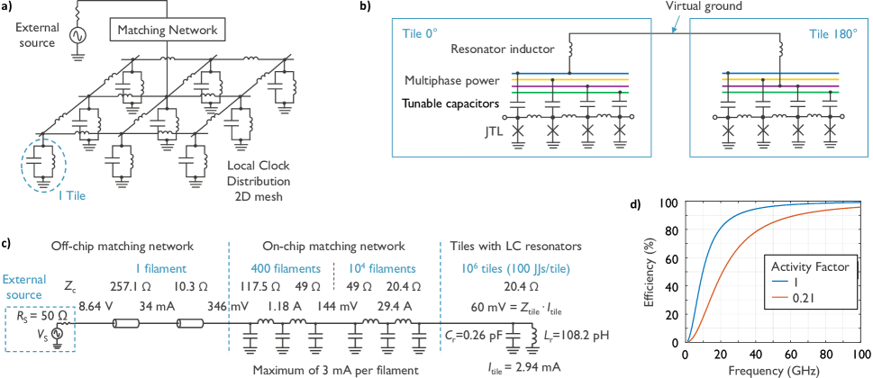
The power layers of the fabrication stack are designed for a high integration density implementation of the AC power network with a 2D array of tightly-coupled local LC resonators as shown in Fig. 2a. The design balances multiple features including density of bias taps, efficient use of metal layers, energy efficiency, clean resonance mode structure, and tunable frequency. The design has a 30 GHz clock frequency and 400 M bias taps per 11 cm2. Density is achieved by shunting the JJs with lumped LC resonators as shown in Fig. 2b. A critical design feature is that inductance scales inversely with number of Josephson junctions. The inductance of a combined 100 taps is 10,000 times smaller than that of 100 individual taps. In the proposed stack, a 55 area accommodates 100 JJs with average critical current of 42 A and a corresponding 100 HZO MIM capacitors with an average 2.6 fF. The maximum number of the JJs per tile is set by the bias current through the inductor, which must be within the critical current of the high kinetic inductance wire that scales with wire cross-section. The NbTiN wire with cross-section 200 nm200 nm has a critical current up to 5 mA. This constraint sets the number of junctions per tile.
Scaling the design to 30 GHz and large chip area of 11 cm2 is achieved by coupling LC tiles with a 2D inductive mesh. This ideal network presents a zero-order mode resonance with uniform amplitude and phase. The LC resonance frequencies however changes over larger chip areas due to variation in materials and processes. Tuneable HZO capacitors are therefore introduced to improve homogeneity of the resonance frequency across-chip. Capacitance is tuned over 10% by adjusting the DC bias across the capacitor.
Practical aspects of the design include the feed network, illustrated in Fig. 2c, that transforms impedance and stabilizes the desired zero-order mode. The impedance of an individual LC resonator tile is two orders of magnitude higher than the characteristic impedance of the biased JJs, but the impedance of 4 M tiles in parallel is still much lower than the 50 source. Implementation of the feed network is based on the same lumped-LC layout style as the primary resonators, with a progressive decrease in the number of tiles per stage in the feed network, producing the corresponding increase in impedance. In this way a hierarchical structure of LC resonators is formed. The number of connections between layers is optimized to cancel parasitic resonances by providing a regular grid of feed points, and to keep current at any point of the network below 3 mA. Inductance of the 2D mesh is invariant between all layers of the feed network. Capacitance at the highest level is dominated by mesh-based parasitics to the ground, which the design must take into account.
Another constraint on the power distribution is amplitude stability across variable JJ switching activity. High switching activity loads the network and reduces amplitude. The variation can be expressed as
| (1) |
with the quality factor of the external 50 source at room temperature and the quality factor of the JJ dynamic switching. Stability is guaranteed when the external quality factor of the resonator is sufficiently low compared to the quality factor of dynamic switching. The desired external quality factor is achieved in the design of the matching network.
Not all AC power from the LC resonators is consumed by switching JJs. Part of it is lost inside the capacitor and inductor of the resonator. Well below the critical temperature, the loss in the NbTiN inductor is so low Mazin (2020) that only the loss in the capacitpr dielectric is significant. The quality factor of the material loss is therefore , the inverse of the loss tangent of the capacitor dielectric. The useful power consumed by the switching JJs has an associated quality factor with the activity factor and the clock frequency. , and are parameters for a 55 m2 tile of 100 switching JJs: is the resonator capacitance for one tile, and are respectively the total bias current and total switching energy for 100 JJs in one tile. The efficiency of the power distribution is
| (2) |
The efficiency is dependent on the activity factor and improves with clock frequency as shown in Fig. 2d. The dynamic power consumption of the JJs is determined with a bias current of 2.94 mA and energy consumption of 2.87 aJ for 100 JJs in one tile. A tile capacitor of 0.26 pF with a loss tangent of 10-4 is used in the efficiency calculation. At 30 GHz, efficiency of 90% is achieved at a high activity factor of 1, and 65% is achieved at an activity factor of 0.21 that corresponds to the practical case in efficient logic designs.
IV Flux Trapping
Advanced materials and fabrication development would be incomplete without characterization of flux trapping, which causes variability in the circuit cooldown to cooldown. This has historically been a dominant failure mechanism. Pearl vortices form in the ground plane during cooldown through the superconducting transition temperature Pearl (1964), producing parasitic-flux coupling to the active circuit. The parasitic coupling is up to one-half of an SFQ, , if the vortex is located directly under the wire.
Ginzburg-Landau theory Tinkham (2004) describes the physics of vortex motion. Two characteristic energies and two material constants determine vortex dynamics: magnetic field energy that depends on London penetration depth, and pinning energy that depends on coherence length. In practice, defectivity of the material affects pinning energy and viscosity of the vortex Dhakal, Ciovati, and Gurevich (2020). The potential of the vortex can be calculated analytically in simple cases Brandt (2006); Shmidt and Mkrtchyan (1974) and can be simulated in complex geometries Kartsev (2018); Blair et al. (2021); Sadovskyy et al. (2015). The materials aspect of flux trapping has been studied in the cavity and high current communities, as unpinned vortices are a major source of loss and reduced critical current Liarte et al. (2018); Giroud et al. (1992). These communities have put extensive effort into material optimization and characterization of pinning parameters.
The effort in the digital community has been on design of ground plane voids, or moats, to attract and sequester the flux. Moat design has been treated empirically through the scanning squid microscopy measurements Kirtley (2010) of different geometries Bermon and Gheewala (1983); Jeffery et al. (1995). Historically, moat design was not fully effective simply because the moats were spaced too far apart. A conceptual breakthrough occurred when patterned strips of Nb less than 20 m wide were shown to completely expel flux Stan, Field, and Martinis (2004). In the context of ICs, this translates to long moats spaced less than 20 m apart, which have been effective for large, linear circuits Herr et al. (2015); Semenov, Polyakov, and Tolpygo (2017). Long moats are incompatible with X-Y routing in large circuits. Instead, a regular grid of smaller moats has been adopted with established design rules for moat coupling Fujiwara et al. (2009); Herr, Talanov, and Herr (2020). Alternately, design tools Fourie et al. (2019) and modeling Semenov and Khapaev (2016) have been proposed to evaluate ad-hoc moat placement, but these tools consider only the magnetic energy of the vortex, neglecting material defects.
While mitigations have improved, allowing circuit scale and complexity to increase, the best understandings of parasitic flux mitigation have not been fully implemented due to limitations imposed by materials and fabrication. Flux mitigation must start with the fabrication stack including material stability and control, enabling dedicated ground planes with a relatively high critical temperature Semenov and Khapaev (2016), electrically isolated from the rest of the circuit Herr, Talanov, and Herr (2020). The miniaturization that comes with advanced fabrication nodes would only improve flux performance by placing the moats closer together. The fabrication stack described here answers to all the above. NbTiN ground planes top and bottom have critical temperature that can be engineered with material composition.
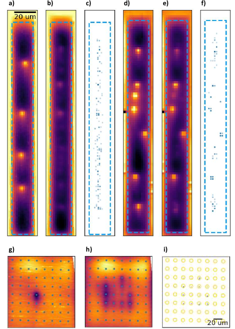
Fig. 3 shows flux images of the NbTiN ground plane fabricated in the same process as the wires and patterned into either strips or a grid of holes. Images can be directly compared to similar experiments done with Nb Stan, Field, and Martinis (2004); Grigorenko et al. (2001); Chiaro et al. (2016). The primary figure of merit in these experiments is the critical field, corresponding to onset of the first vortex trapped in the ground plane. The critical field as function of strip width is a direct measure of the material parameters of the film Stan, Field, and Martinis (2004); Clem and Kogan (2012); Likharev (1971). The critical field of the 10 m NbTiN strip, T, is less than the published value for Nb, T for a film thickness of 210 nm. The measured critical field for NbTiN depends on the film thickness, 45 T for 50 nm and 40 T for 100 nm. The decrease in critical field relative to Nb follows an increase of the Ginsburg-Landau constant for a coherence length of 5 nm Valente-Feliciano et al. (2015) and penetration depth of 380 nm estimated from the normal-state resistivity and superconducting critical temperature of the films Bartolf (2015).
The NbTiN images in Fig. 3 show that internal defectivity of the material is quite low. Internal pinning of the material is characterized by distances from a trapped vortex to the centerline and to the edge of the strip. The position of the vortices in the 100 nm film are near the centerline and there are no consistent pinning centers. The 50 nm film images do show consistent defects, including one that is close to the edge of the film. The difference between the two films might be explained by columnar growth of NbTiN film with grain boundaries averaging out with an increase of the thickness. Finally, the patterned ground plane with 0.5 m holes spaced 20 m apart shows consistent pinning in the holes at an applied field up to 240 nT, typical of digital circuits in a passively shielded environment. The hole size and spacing is consistent with high integration density of the stack consuming less than 1% of the total area on the chip and allowing for dense routing with minimal blockages.
V Conclusion
We have proposed a superconductor integrated circuit fabrication stack with a materials set that provides a foundation for 400 MJJ/cm2 integration scale in digital superconducting circuits. Fabrication processes for NbTiN wireup, low-capacitance -silicon barrier JJs, and low loss, high- tunable HZO capacitors are compatible with 300 mm CMOS processes and thermal budgets. The stack uses standard inter-layer dielectric processes and 28 nm lithography. Initial fabrication and test cycles have shown wires with properties meeting the design requirements and good flux trapping properties sufficient for large scale integrated circuits. Further development is progressing with Josephson junctions and MIM capacitors. The fabrication stack has been codeveloped with a resonant clock network scalable for 400M taps in a chip area of 11 cm2 and clock frequency of 30 GHz. In a companion paper Herr, Josephsen, and Herr (ress) we present circuit designs for logic and memory built on this foundation.
Acknowledgements.
Work at imec and imec USA is supported by imec INVEST+ and by Osceola County. Work at Cornell is supported by the Cornell Center for Materials Research with funding from the NSF MRSEC program (DMR-1719875). Work at Jefferson Laboratory is supported by the U.S. Department of Energy, Office of Science, and Office of Nuclear Physics under Contract No. DE-AC05-06OR23177.References
References
- Strubell, Ganesh, and McCallum (2020) E. Strubell, A. Ganesh, and A. McCallum, in Proceedings of the AAAI Conference on Artificial Intelligence, Vol. 34 (2020) pp. 13693–13696.
- Li et al. (2020) T. Li, J. Hou, J. Yan, R. Liu, H. Yang, and Z. Sun, Electronics 9, 670 (2020).
- Ilderem (2020) V. Ilderem, Nature Electronics 3, 5 (2020).
- Ayala et al. (2021) A. Ayala, S. Tomov, M. Stoyanov, and J. Dongarra, in International Conference on Parallel Computing Technologies (Springer, 2021) pp. 279–287.
- McDermott et al. (2018) R. McDermott, M. Vavilov, B. Plourde, F. Wilhelm, P. Liebermann, O. Mukhanov, and T. Ohki, Quantum science and technology 3, 024004 (2018).
- Wustmann and Osborn (2020) W. Wustmann and K. D. Osborn, Physical Review B 101, 014516 (2020).
- Kuncic and Nakayama (2021) Z. Kuncic and T. Nakayama, Advances in Physics: X 6, 1894234 (2021).
- Yohannes et al. (2005) D. Yohannes, S. Sarwana, S. K. Tolpygo, A. Sahu, Y. A. Polyakov, and V. K. Semenov, IEEE transactions on applied superconductivity 15, 90 (2005).
- Berkley et al. (2010) A. Berkley, M. Johnson, P. Bunyk, R. Harris, J. Johansson, T. Lanting, E. Ladizinsky, E. Tolkacheva, M. Amin, and G. Rose, Superconductor Science and Technology 23, 105014 (2010).
- Tolpygo et al. (2014a) S. K. Tolpygo, V. Bolkhovsky, T. J. Weir, L. M. Johnson, M. A. Gouker, and W. D. Oliver, IEEE transactions on Applied Superconductivity 25, 1 (2014a).
- Egan, Brownfield, and Herr (2022) J. Egan, A. Brownfield, and Q. Herr, Superconductor Science and Technology 35, 045018 (2022).
- (12) A. Y. Herr (Presented at the Applied Superconductivity Conference, Washington State Convention Center, Seattle, WA, October 30, 2018.).
- Pinto et al. (2018) N. Pinto, S. J. Rezvani, A. Perali, L. Flammia, M. V. Milošević, M. Fretto, C. Cassiago, and N. De Leo, Scientific reports 8, 1 (2018).
- Gupta et al. (2016) V. Gupta, J. A. Sellers, C. D. Ellis, S. Zou, G. A. Hernandez, R. Bai, Y. Cao, D. B. Tuckerman, and M. C. Hamilton, in Proc. IMAPS 12th Int. Conf. Exhib. Device Packag. (2016) pp. 002075–002094.
- Gubin et al. (2005) A. Gubin, K. Il’in, S. Vitusevich, M. Siegel, and N. Klein, Physical Review B 72, 064503 (2005).
- Tolpygo et al. (2021) S. K. Tolpygo, E. B. Golden, T. J. Weir, and V. Bolkhovsky, Superconductor Science and Technology 34, 085005 (2021).
- Tolpygo et al. (2014b) S. K. Tolpygo, V. Bolkhovsky, T. Weir, C. Galbraith, L. M. Johnson, M. A. Gouker, and V. K. Semenov, IEEE Transactions on Applied Superconductivity 25, 1 (2014b).
- Tolpygo and Semenov (2020) S. K. Tolpygo and V. K. Semenov, in Journal of Physics: Conference Series, Vol. 1559 (IOP Publishing, 2020) p. 012002.
- Yogi and Mercereau (1981) T. Yogi and J. Mercereau, IEEE Transactions on Magnetics 17, 931 (1981).
- Crauste et al. (2013) O. Crauste, A. Gentils, F. Couëdo, Y. Dolgorouky, L. Bergé, S. Collin, C. Marrache-Kikuchi, and L. Dumoulin, Physical Review B 87, 144514 (2013).
- Verjauw et al. (2021) J. Verjauw, A. Potočnik, M. Mongillo, R. Acharya, F. Mohiyaddin, G. Simion, A. Pacco, T. Ivanov, D. Wan, A. Vanleenhove, et al., Physical Review Applied 16, 014018 (2021).
- Amparo and Tolpygo (2010) D. Amparo and S. K. Tolpygo, IEEE transactions on applied superconductivity 21, 126 (2010).
- Lindemann, Radecker, and Sperlich (2007) H. Lindemann, J. Radecker, and H.-P. Sperlich, in 2007 IEEE/SEMI Advanced Semiconductor Manufacturing Conference (IEEE, 2007) pp. 253–258.
- Tolpygo et al. (2017) S. K. Tolpygo, V. Bolkhovsky, S. Zarr, T. Weir, A. Wynn, A. L. Day, L. Johnson, and M. Gouker, IEEE Transactions on Applied Superconductivity 27, 1 (2017).
- Likharev (1985) K. Likharev, Moscow Izdatel Nauka (1985).
- Migacz and Huber (2003) J. V. Migacz and M. E. Huber, IEEE transactions on applied superconductivity 13, 123 (2003).
- Semenov, Polyakov, and Tolpygo (2017) V. K. Semenov, Y. A. Polyakov, and S. K. Tolpygo, IEEE Transactions on Applied Superconductivity 27, 1 (2017).
- Herr et al. (2015) Q. P. Herr, J. Osborne, M. J. Stoutimore, H. Hearne, R. Selig, J. Vogel, E. Min, V. V. Talanov, and A. Y. Herr, Superconductor Science and Technology 28, 124003 (2015).
- Tolpygo (2016) S. K. Tolpygo, Low Temperature Physics 42, 361 (2016).
- Olaya et al. (2010) D. Olaya, P. D. Dresselhaus, S. P. Benz, A. Herr, Q. P. Herr, A. G. Ioannidis, D. L. Miller, and A. Kleinsasser, Applied Physics Letters 96, 213510 (2010).
- Gudkov, Kupriyanov et al. (2012) A. Gudkov, M. Y. Kupriyanov, et al., Journal of Experimental and Theoretical Physics 114, 818 (2012).
- (32) P. Farrell, S. Shauck, B. Konigsburg, S. Rahman, P. Tschirhart, M. Vesely, and R. Clarke (Presented at the Applied Superconductivity Conference, Washington State Convention Center, Seattle, WA, October 29, 2018.).
- (33) M. Vesely (Presented at the Applied Superconductivity Conference, Washington State Convention Center, Seattle, WA, October 29, 2018.).
- Egan et al. (2022) J. Egan, M. Nielsen, J. Strong, V. Talanov, E. Rudman, B. Song, Q. Herr, and A. Herr, Superconductor Science and Technology 35, 105010 (2022).
- Ayala et al. (2020) C. L. Ayala, T. Tanaka, R. Saito, M. Nozoe, N. Takeuchi, and N. Yoshikawa, IEEE Journal of Solid-State Circuits 56, 1152 (2020).
- Strong et al. (2020) J. A. Strong, J. M. Acevdeo, A. K. Sirota, and M. E. Nielsen, “Capacitive clock distribution system,” (2020), uS Patent 10,754,371.
- Herr, Herr, and Strong (2020) A. Y. Herr, Q. P. Herr, and J. A. Strong, “Capacitively coupled superconducting integrated circuits powered using alternating current clock signals,” (2020), uS Patent 10,608,044.
- Herr et al. (2013) A. Y. Herr, Q. P. Herr, O. T. Oberg, O. Naaman, J. X. Przybysz, P. Borodulin, and S. B. Shauck, Journal of Applied Physics 113, 033911 (2013).
- Hosoya et al. (1991) M. Hosoya, W. Hioe, J. Casas, R. Kamikawai, Y. Harada, Y. Wada, H. Nakane, R. Suda, and E. Goto, IEEE Transactions on Applied Superconductivity 1, 77 (1991).
- Strong et al. (2022) J. A. Strong, V. V. Talanov, M. E. Nielsen, A. C. Brownfield, N. Bailey, Q. P. Herr, and A. Y. Herr, Nature Electronics 5, 171 (2022).
- Herr, Josephsen, and Herr (ress) Q. Herr, T. Josephsen, and A. Herr, Applied Physics Letters (in press).
- Kroger, Potter, and Jillie (1979) H. Kroger, C. Potter, and D. Jillie, IEEE Transactions on Magnetics 15, 488 (1979).
- Kroger et al. (1985) H. Kroger, L. Smith, D. Jillie, J. Thaxter, R. Aucoin, L. Currier, C. Potter, D. Shaw, and P. Willis, IEEE Transactions on Magnetics 21, 870 (1985).
- Baek, Dresselhaus, and Benz (2006) B. Baek, P. D. Dresselhaus, and S. P. Benz, IEEE transactions on applied superconductivity 16, 1966 (2006).
- Shan, Sekimoto, and Noguchi (2016) W. Shan, Y. Sekimoto, and T. Noguchi, IEEE Transactions on Applied Superconductivity 26, 1 (2016).
- Valente-Feliciano et al. (2015) A.-M. Valente-Feliciano, G. V. Eremeev, C. E. Reece, J. K. Spradlin, M. C. Burton, and R. Lukaszew, “Growth and characterization of multi-layer NbTiN films,” Tech. Rep. (Thomas Jefferson National Accelerator Facility (TJNAF), Newport News, VA …, 2015).
- Mazin (2020) B. A. Mazin, in Handbook of Superconductivity (CRC Press, 2020) pp. 756–765.
- Hähnle et al. (2021) S. Hähnle, K. Kouwenhoven, B. Buijtendorp, A. Endo, K. Karatsu, D. Thoen, V. Murugesan, and J. Baselmans, Physical Review Applied 16, 014019 (2021).
- Valente-Feliciano et al. (2020) A. Valente-Feliciano, D. Beverstock, C. Reece, et al., (2020).
- Shu et al. (2021) S. Shu, N. Klimovich, B. H. Eom, A. Beyer, R. B. Thakur, H. Leduc, and P. Day, Physical Review Research 3, 023184 (2021).
- Swails (2018) N. S. Swails, Depairing current density in NbTiN superconducting films, Ph.D. thesis, University of South Carolina (2018).
- Cyberey et al. (2019) M. E. Cyberey, T. Farrahi, M. Eller, J. Lu, R. M. Weikle, O. Noroozian, and A. W. Lichtenberger, IEEE Transactions on Applied Superconductivity 29, 1 (2019).
- Clem and Kogan (2012) J. R. Clem and V. Kogan, Physical Review B 86, 174521 (2012).
- Pokhrel et al. (ress) A. Pokhrel, A. Guptal, M.-S. Kim, J.-P. Soulie, S. K. Sarkar, Y. Canvel, V. Renaud, B. Kenens, B. Hodges, S. O’Neal, Q. Herr, A. Herr, and Z. Tökei, in IEEE International Interconnect Technology Conference (IEEE, in press).
- Murdoch et al. (2020) G. Murdoch, Z. Tokei, S. Paolillo, O. V. Pedreira, K. Vanstreels, and C. J. Wilson, in 2020 IEEE International Interconnect Technology Conference (IITC) (IEEE, 2020) pp. 4–6.
- Bartolf (2015) H. Bartolf, in Fluctuation Mechanisms in Superconductors: Nanowire Single-Photon Counters, Enabled by Effective Top-Down Manufacturing (Springer, 2015) pp. 181–184.
- Schenk et al. (2013) T. Schenk, S. Mueller, U. Schroeder, R. Materlik, A. Kersch, M. Popovici, C. Adelmann, S. Van Elshocht, and T. Mikolajick, in 2013 Proceedings of the European Solid-State Device Research Conference (ESSDERC) (IEEE, 2013) pp. 260–263.
- Aldrigo et al. (2020) M. Aldrigo, M. Dragoman, S. Iordanescu, F. Nastase, and S. Vulpe, Nanomaterials 10, 2057 (2020).
- Choi, Mao, and Chang (2011) J. Choi, Y. Mao, and J. Chang, Materials Science and Engineering: R: Reports 72, 97 (2011).
- Lin et al. (2020) Y. W. Lin, K. Mizutani, T. Hoshii, H. Wakabayashi, K. Tsutsui, Y.-F. Tsao, T.-J. Huang, H.-T. Hsu, and K. Kakushima, ECS Transactions 98, 71 (2020).
- Woo (2021) J. Woo, in 2021 IEEE International Symposium on Circuits and Systems (ISCAS) (IEEE, 2021) pp. 1–4.
- Yurchuk et al. (2014) E. Yurchuk, J. Müller, J. Paul, T. Schlösser, D. Martin, R. Hoffmann, S. Müeller, S. Slesazeck, U. Schröeder, R. Boschke, et al., Ieee Transactions on Electron Devices 61, 3699 (2014).
- McRae et al. (2020) C. R. H. McRae, H. Wang, J. Gao, M. R. Vissers, T. Brecht, A. Dunsworth, D. P. Pappas, and J. Mutus, Review of Scientific Instruments 91, 091101 (2020).
- Pearl (1964) J. Pearl, Applied Physics Letters 5, 65 (1964).
- Tinkham (2004) M. Tinkham, Introduction to superconductivity (Courier Corporation, 2004).
- Dhakal, Ciovati, and Gurevich (2020) P. Dhakal, G. Ciovati, and A. Gurevich, Physical Review Accelerators and Beams 23, 023102 (2020).
- Brandt (2006) E. Brandt, Physica C: Superconductivity and its applications 437, 29 (2006).
- Shmidt and Mkrtchyan (1974) V. Shmidt and G. Mkrtchyan, Soviet Physics Uspekhi 17, 170 (1974).
- Kartsev (2018) P. F. Kartsev, in Proceedings of the International Workshop on OpenCL (2018) pp. 1–2.
- Blair et al. (2021) A. Blair et al., Simulations of Critical Currents in Polycrystalline Superconductors Using Time-Dependent Ginzburg–Landau Theory, Ph.D. thesis, Durham University (2021).
- Sadovskyy et al. (2015) I. Sadovskyy, A. Koshelev, C. L. Phillips, D. A. Karpeyev, and A. Glatz, Journal of Computational Physics 294, 639 (2015).
- Liarte et al. (2018) D. B. Liarte, D. Hall, P. N. Koufalis, A. Miyazaki, A. Senanian, M. Liepe, and J. P. Sethna, Physical Review Applied 10, 054057 (2018).
- Giroud et al. (1992) M. Giroud, O. Buisson, Y. Wang, B. Pannetier, and D. Mailly, Journal of low temperature physics 87, 683 (1992).
- Kirtley (2010) J. Kirtley, Reports on Progress in Physics 73, 126501 (2010).
- Bermon and Gheewala (1983) S. Bermon and T. Gheewala, IEEE Transactions on Magnetics 19, 1160 (1983).
- Jeffery et al. (1995) M. Jeffery, T. Van Duzer, J. Kirtley, and M. Ketchen, Applied Physics Letters 67, 1769 (1995).
- Stan, Field, and Martinis (2004) G. Stan, S. B. Field, and J. M. Martinis, Physical review letters 92, 097003 (2004).
- Fujiwara et al. (2009) K. Fujiwara, S. Nagasawa, Y. Hashimoto, M. Hidaka, N. Yoshikawa, M. Tanaka, H. Akaike, A. Fujimaki, K. Takagi, and N. Takagi, IEEE transactions on applied superconductivity 19, 603 (2009).
- Herr, Talanov, and Herr (2020) A. Y. Herr, V. V. Talanov, and Q. P. Herr, “Superconductor ground plane patterning geometries that attract magnetic flux,” (2020), uS Patent App. 16/296,007.
- Fourie et al. (2019) C. J. Fourie, K. Jackman, M. M. Botha, S. Razmkhah, P. Febvre, C. L. Ayala, Q. Xu, N. Yoshikawa, E. Patrick, M. Law, et al., IEEE Transactions on Applied Superconductivity 29, 1 (2019).
- Semenov and Khapaev (2016) V. K. Semenov and M. M. Khapaev, IEEE Transactions on Applied Superconductivity 26, 1 (2016).
- Grigorenko et al. (2001) A. Grigorenko, G. Howells, S. Bending, J. Bekaert, M. Van Bael, L. Van Look, V. Moshchalkov, Y. Bruynseraede, G. Borghs, I. Kaya, et al., Physical review b 63, 052504 (2001).
- Chiaro et al. (2016) B. Chiaro, A. Megrant, A. Dunsworth, Z. Chen, R. Barends, B. Campbell, Y. Chen, A. Fowler, I. Hoi, E. Jeffrey, et al., Superconductor Science and Technology 29, 104006 (2016).
- Likharev (1971) K. Likharev, Radiophysics and Quantum Electronics 14, 722 (1971).