Twisted cuprate van der Waals heterostructures with controlled Josephson coupling
Abstract
Twisted van der Waals (vdW) heterostructures offer a unique platform for engineering the efficient Josephson coupling between cuprate thin crystals harboring the nodal superconducting order parameter. Preparing the vdW heterostructures-based Josephson junction comprising stacked cuprates requires maintaining an ordered interface with preserved surface superconductivity. Here, we report the preparation of the Josephson junction out of the stacked crystals using the cryogenic dry transfer technique and encapsulating the junction with an insulating layer, that protects the interface during the electrical contacts evaporation at the base pressure. We find that the Josephson critical current has a maximum at low twist angles, comparable to that of the bulk intrinsic Josephson junctions, and is reduced by two orders of magnitude at twist angles close to . The reduction of occurs due to a mismatch between superconducting -wave order parameters, which suppresses the direct Cooper pair tunneling.
pacs:
Valid PACS appear hereI Introduction
Twisted van der Waals (vdW) heterostructures comprising thin cuprate superconductors have been proposed as an adaptable platform for Josephson junctions (JJs) with controllable properties [1, 2, 3, 4, 5, 6]. These structures offer a unique opportunity for revealing an interplay between superconducting order parameter (SOP) symmetries in the superconducting crystals. The cuprate compound, (BSCCO) represents an ideal system for realizing the vdW heterostructures. Such a heterostructure forms a stack of the intrinsic JJs along the BSCCO crystallographic -axis, comprising the superconducting CuO2 bilayers sandwiched between the insulating [SrO-BiO] bilayers [7]. Cleaving the BSCCO between the BiO planes forms atomically thin crystals with the superconducting transition temperature as high as that of bulk [8, 9, 10], holding the -wave superconducting gap [11, 12]. Because of the nodal gap in the -wave SOP [13, 14], the Josephson tunneling across the twisted BSCCO junctions is expected to be suppressed at certain angles. Nevertheless, past experiments on the twisted BSCCO junctions did not detect any angular dependence of the Josephson critical current [17, 15, 16]. This can be understood as a result of the high-temperature annealing in oxygen, which not only restores the surface superconductivity but also induces the undesired structural distortions at the junction. At the same time, the strong angular dependence of the critical current compatible with the -wave pairing symmetry has been reported on the micron-thick whisker BSCCO junctions [18]. The -wave nature of the SOP has been also demonstrated in the grain boundary (GB)-based cuprate JJs and superconducting quantum interference devices fabricated using the bicrystal and tricrystal techniques [20, 19, 21, 22]. The symmetry of the SOP was easy to observe in the GB junctions since the in-plane coherence length is much larger than the coherence length along the -axis. Yet, the GBJJs have inevitable multifaceted interfaces in all three dimensions that create additional complexity in controlling Josephson coupling [23].
Furthermore, the small, 0.1 nm [24], BSCCO -axes coherence length, the high mobility oxygen dopants above [26, 25], and the chemical reactivity of the oxygen under an ambient atmosphere in the thin BSCCO crystals [28, 27] hinder the realization of vertical heterostructures with coherent interfaces free of detrimental disorder. An innovative cryogenic stacking technique in an inert atmosphere has recently enabled the atomically flat interface between twisted BSCCO crystals with preserved interfacial superconductivity [29, 30]. In the resulting JJs, the critical current exhibited a strong angular dependence compatible with the -wave SOP and an unusual non-monotonic temperature behavior due to the unconventional sign change of the nodal superconducting gap [3, 5]. Around where the -wave SOP of the two crystals mismatch maximally, the remaining superconducting coherence was ascribed to the presence of a finite second harmonics in the Josephson current-phase relation associated with co-tunneling of Cooper pairs across the junction [3, 5]. The second harmonics was identified through the observation of fractional Shapiro steps and the analysis of the Fraunhofer patterns [29]. Time-Reversal Symmetry broken phases in twisted bilayers of cuprate high-temperature superconductors [31, 4, 32, 33, 34, 35] have been theoretically proposed, potentially leading to the chiral Majorana modes [36, 37].
Here, we build several JJs with different twist angles using the recently established dry and cryogenic stacking technique [29]. We encapsulate the junction region with an insulating crystal which enables us to prevent the detrimental effects of disorder during the device fabrication [38], especially during the evaporation of electrical contacts in high-vacuum. Since our chamber has a base pressure of and is not under the high-vacuum condition as in Ref. [29], the reactivity of water molecules during the metal deposition is still too high. Therefore, an additional encapsulating layer is essential for preserving a pristine interface between the thin BSCCO crystals. By doing so, we also extend the lifetime of the device for several days.
II Fabrication of high-quality Josephson Junctions
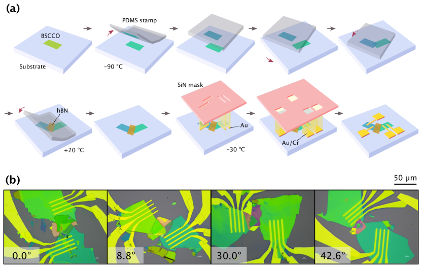
We fabricate seven JJs devices consisting of two BSCCO crystals with a controlled twist angle using the cryogenic stacking technique in a glove box filled with argon. The twist angle ranges below : two samples have , two samples have twist angle close to ( and ) and three samples are twisted at intermediate angles (). The key steps of the JJ fabrication are sketched in Fig. 1(a), and the details of the technique are presented in Ref. [29]. First, an optimally doped BSCCO flake is mechanically exfoliated using the scotch tape on SiO2/Si, previously treated with the oxygen plasma to enhance the vdW forces between the crystal and the substrate [27]. Next, the BSCCO flake is placed on a liquid nitrogen-cooled stage and cleaved into two pieces using a polydimethylsiloxane (PDMS) stamp at -. At this low temperature, the oxygen atoms in the BiO planes are frozen and no interfacial structural reconstruction occurs [39]. The substrate is then quickly rotated to the desired angle and the flake on the PDMS is stacked on top of the other one. Less than 60 seconds elapse between the cleavage of the starting crystal and the assembly of the two parts. The stack is then warmed up to room temperature and released onto the substrate by gently lifting up the PDMS stamp. Immediately afterwards, we encapsulate the interface region with the hexagonal boron nitride thick layer via the PDMS transfer technique process in order to prevent the degradation at the junction resulting from chemical reactions with water or oxygen escape. Finally, electrical contacts are defined via stencil masks [10] and deposited at - in two steps in the evaporation chamber directly connected to the glovebox. Gold contacts are first established on the BSCCO flake, whereas the gold contacting pads are subsequently deposited with the chromium adhesion layer. To avoid local heating that causes loss of oxygen dopants the evaporation rate is set as low as fractions of . This implies that each deposition lasts around 3 hours, including the pumping and the venting of the chamber. The two steps evaporation aims at avoiding Cr directly onto the flakes since Cr oxidizes by ripping off oxygen molecules from the BSCCO. This undesired chemical reaction would lead to an insulating behavior of the region underlying the contact layer, strongly degrading the superconducting properties of the entire device [40]. Using this protocol, we obtain the high-quality electrical contact with the areal resistance smaller than , an order of magnitude lower than the contact resistance resulting from a single evaporation (Au/Cr) on BSCCO under our conditions. Figure 1(b) displays four representative twisted-JJs devices investigated in this study. All the flakes show a similar optical color contrast which corresponds to the thickness range of 30-. According to our experience and under our experimental conditions, below this thickness the JJ is of lower electronic quality or not entirely superconducting, possibly due to the lower robustness of each flake and due to the high spatial atomic modulation in thin crystals that affects the flatness of the interface.
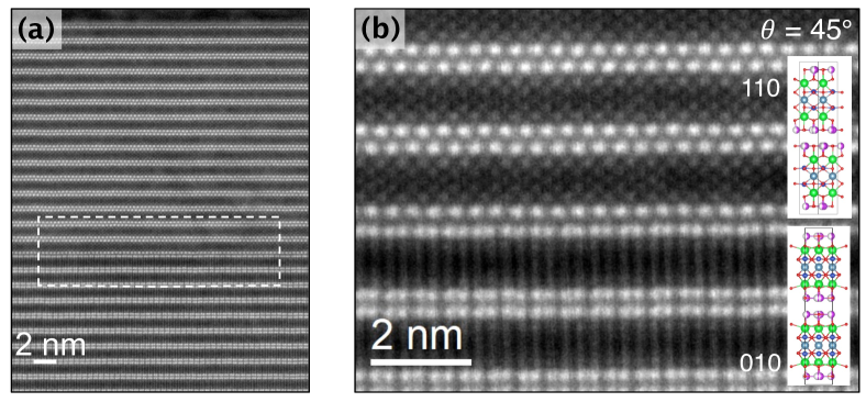
To demonstrate the sharpness of our twisted interfaces at the atomic resolution, we perform cross-sectional high-annular dark-field scanning transmission electron microscopy in an extra heterostructure twisted at . Bright spots in Fig. 2 correspond to electron scattering on atomic columns, the brightest of which are Bi that terminate each vdW layer and are the ones fully resolved. The crystalline order of each crystal is clearly preserved at the interface.
Figure 3(a) shows the electrical resistance across each of the seven junctions, measured injecting -current in the four-terminal geometry as a function of temperature . The temperature dependence of each resistance exhibits a linear behavior in the normal state, consistent with the optimally doped [8]. The of the JJs devices is followed by the clear single superconducting (SC) transition occurring at the temperature slightly lower than the bulk critical temperature of [41], indicating optimal oxygen doping even at the junction interface. The only exception is given by the JJ with , whose electrical resistance displays a tiny hump between and , suggesting a slightly underdoped interface. The devices investigated in this study have an onset superconducting critical temperature between and with the average value of [inset of 3(a)]. Through this study, refers indeed to the highest temperature at which the electrical resistance measured across the junction remains zero (marked by a triangle in Fig. 3(a) for two representative JJs). We observe no correlation between and the twist angle. We ascribe instead the variability of to a different, albeit reduced, oxygen loss at the cleaved surface during the exfoliations, as far as the flakes are thick enough to guarantee a flat interface that allows coherent tunneling of Cooper pairs through the junction.
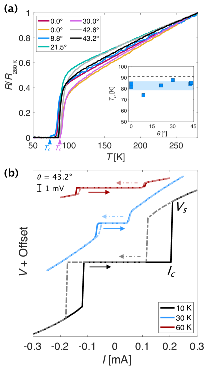
Inset of (a): Angle dependence of of corresponding the corresponding JJs. The blue-shaded area is around the mean value of the critical temperatures and its width is two times the standard deviation. The black dashed line indicates the of an optimally doped bulk BSCCO crystal. (b) Current-voltage (-) characteristics of a -twisted JJ measured by sweeping the current in both directions (arrows) at , and .
The current-voltage (-) characteristics of a representative JJ with measured at three different temperatures are displayed in [Fig. 3(b)]. The sharp SC transition across the JJs, especially visible at , confirms significant switching at the interface. As we sweep the electrical current from a large negative value, the junction voltage first retraps to the SC state () and then jumps to the resistive state at the critical current . The switching voltage at is . At low temperatures, the - curve of the JJ exhibits the large hysteresis in the bias current sweep, directly associable to the dielectric nature of the tunnel barrier with the high capacitance in the underdamped regime [42]. By reversing the current polarity, we obtain the - characteristic mirrored along the axis. As shown in Fig. 3(b), the hysteresis becomes weaker as the temperature is increased, in agreement with previous studies on intrinsic JJs.
III Results & Discussion
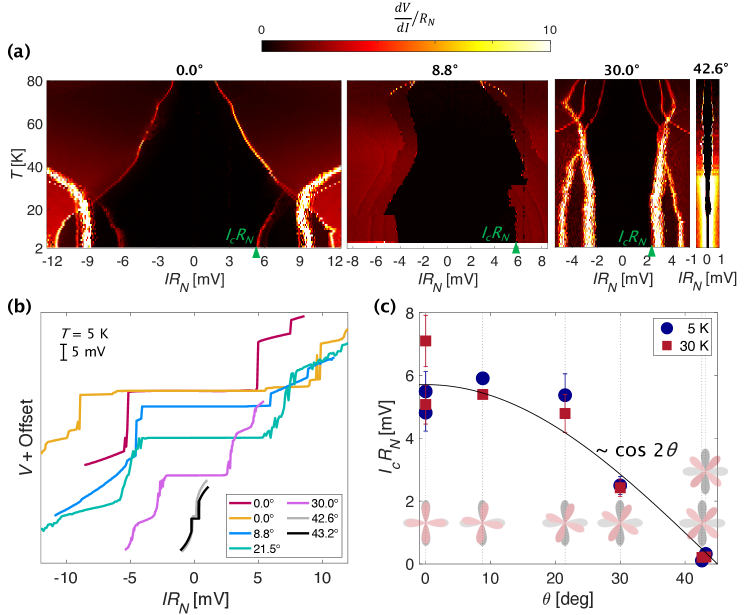
We investigate the pairing symmetry of the Cooper pairs in the twisted BSCCO JJs by measuring the - characteristics and the dynamic resistance across the interface for several twisted JJs. We sweep a dc bias from a negative to positive value while superimposing a tiny alternating current of amplitude with the frequency of , and measure simultaneously the dc and ac voltages across each junction. The details of the measurement are reported in the Supplementary Information. To compare the transport data of all the JJs, we normalize the bias current as , where is the junction resistance in the normal state, estimated as the slope of the - curve in the linear region. Since both and scale linearly with the junction area, their product is independent of it. Figure 4(a) illustrates the normalized differential resistance as a function of and temperature for four representative twisted JJs. Similar data for all seven JJs are included in Fig. S2 in the Supplementary Information (SI). The main feature that can be deduced from the color plots is that , at which the inner peaks of each appear, sensitively decreases at twist angles close to .
For better visualization, we show in Fig. 4(b) the characteristics at in all the samples. For the two JJs with , the critical currents normalized by the corresponding junction area are and at [38], comparable to of intrinsic junction in BSCCO crystals, which ranges at that temperature from to , depending on the number of junctions along the -axis [43]. The realization of pristine interfaces allows us to rule out the effect of detrimental disorder at the junctions arising during the fabrication process, and to attribute any changes of to the intrinsic effects of the BSCCO SOP symmetry. Differently from BSCCO JJs investigated in previous studies [29, 30], the at in Fig 4(a) does not show hysteresis, suggesting a barrier with low capacitance. On the other hand, some of the JJs with finite twist angles show an asymmetric with respect to , displaying a difference in amplitude between the critical current and the retrapping current, appearing in the underdamped region, see Fig. S2 in the SI. The amount of damping is generally insensitive to the angle but it depends on the dielectric nature of the junction’s capacitance. Nevertheless, we observe no correlations, for instance, between the tunneling property (damping regime) and the time between cleaving and stacking the flakes to create the interface, which is comparable for all devices and in all the cases below . One possible factor that determines the capacitance of the barrier is the purity level of argon in the glovebox which could change during the fabrication of the different interfaces. As we do not observe water condensation down to , we estimate the partial pressure of water in the order of 10 ppb. This extremely low density of water molecules might slightly vary depending on the humidity condition of the laboratory due to finite exchange with the glovebox through the butyl gloves. Another factor that could give rise to a difference in the tunnel barrier’s capacitance between the samples is the way the top flake stacks on top of the bottom one within the interface region. Two other important features are visible in the set of the color maps. In the twisted JJs with , the has a nonmonotonic temperature dependence: it increases above , before dropping close to . This behavior can be related to the extrinsic mechanisms active at higher temperatures and/or to the intrinsic competition between the supercurrent contributions from nodal and anti-nodal regions of the Fermi surface driven by tunnel directionality [44].
In the high-temperature regime, the tunneling becomes less coherent at the two contributions that have different magnitudes [5], resulting in a higher net . Secondly, additional peaks in all appear at bias exceeding the critical current, which can be associated either with the multiparticle tunneling [45], such as phonon-assisted tunneling process [46], and to intrinsic JJs intruding the current path between the voltage leads [47].
Figure 4(c) displays the angular dependence of at two representative temperatures and . We notice that follows a dependence, which is the expected behavior of the critical current for tunneling between the -wave superconductors in the first order approximation. The values of in the two JJs with a tilt angle close to are about two orders of magnitude lower than that in the slightly twisted JJs. The critical current is significantly reduced in these two JJs due to the nearly maximum mismatch between the -wave SOPs of the two crystals, but it still remains finite. This feature occurs, on one hand, since the tilt angle is not exactly , but, on the other hand, even if it were, should not completely vanish due to the nonzero contribution of the second harmonic component (at ) to the total critical current [3].
Despite the different temperature profiles of in the seven devices, the behavior of the angular dependence in remains almost unchanged up to . For , is around at , much smaller than the switching voltage amplitude of in the - curve at the same temperature (not shown), which corresponds to the superconducting gap value in the ideal tunnel junctions [42]. This difference arises from the partial incoherent tunneling that does contribute to the conductivity (), but does not affect the of a -wave superconductor. As can be seen from the comparison between the switching voltage in Figs. 3(b) and the magnitude of in Fig. 4(c), this discrepancy () becomes huge for , since the is not really dominated by the twist (especially the incoherent part), but depends crucially on the symmetry of the Cooper pair wavefunction and direct Cooper-pair tunneling is expected to be strongly suppressed at .
IV Conclusions
In summary, we adopt the cryogenic, solvent-free stacking technique to realize interfaces protected with an insulating hBN flake. We investigate the anisotropic SOP of BSCCO by studying the angular dependence of the critical current in the twisted JJs. The superconducting transition of the twisted BSCCO junctions is shown to be very sharp as demonstrated by the temperature dependence of the resistance and the current-voltage characteristics, and occurs at the temperature comparable to the bulk value of . We find that the critical current density in the -JJ is similar to that of the intrinsic JJs and drops by two orders of magnitude when the twist angle approaches , demonstrating the -wave superconducting order parameters.
Data availability
The data that support the findings of this study are available from the corresponding author upon reasonable request.
Acknowledgements. The experiments were partially supported by the Deutsche Forschungsgemeinschaft (DFG 452128813, DFG 512734967, DFG 492704387, DFG 460444718). D.W. acknowledges funding from DFG SFB 1415, Project ID No. 41759051. The work of V.M.V. was supported by the Terra Quantum AG. K.W. and T.T. acknowledge support from the JSPS KAKENHI (Grant Numbers 19H05790, 20H00354 and 21H05233). The work at BNL was supported by the US Department of Energy, office of Basic Energy Sciences, contract no. DOE-sc0012704. The authors are grateful to Heiko Reith and Nicolas Perez for providing access to cleanroom and cryogenic facilities respectively. The authors thank Thomas Wiek and Dina Bieberstein for TEM sample preparation. The authors are also grateful to S. Y. Frank Zhao, Philip Kim, Uri Vool and Valentina Brosco for illuminating and fruitful discussions.
Author contributions. N.P. conceived and designed the experiment; M.M., Y.L., T.C. performed the experiments and analyzed the data. The cuprate crystals have been provided by G.G. The hexagonal boron nitride crystals have been provided by K.W. and T.T. The fabrication procedure and the results have been discussed by N.P., M.M., Y.L. and V.M.V. The manuscript has been written by N.P., M.M., Y.L., V.M.V., and K.N. All authors discussed the manuscript.
Declaration of Interest All authors declare no conflict of interest.
References
- [1] Kawabata, S., Kashiwaya, S., Asano, Y. & Tanaka, Y. Macroscopic quantum tunneling and quasiparticle dissipation in d-wave superconductor Josephson junctions. Physical Review B. 70, 132505 (2004)
- [2] Yokoyama, T., Kawabata, S., Kato, T. & Tanaka, Y. Theory of macroscopic quantum tunneling in high-T c c-axis Josephson junctions. Physical Review B. 76, 134501 (2007)
- [3] Volkov, P., Zhao, S., Poccia, N., Cui, X., Kim, P. & Pixley, J. Josephson effects in twisted nodal superconductors. ArXiv Preprint ArXiv:2108.13456. (2021)
- [4] Can, O., Zhang, X., Kallin, C. & Franz, M. Probing time reversal symmetry breaking topological superconductivity in twisted double layer copper oxides with polar Kerr effect. Phys. Rev. Lett. 127, 157001 (2021)
- [5] Tummuru, T., Plugge, S. & Franz, M. Josephson effects in twisted cuprate bilayers. Physical Review B. 105, 064501 (2022)
- [6] Volkov, P., Wilson, J., Lucht, K. & Pixley, J. Magic angles and correlations in twisted nodal superconductors. Physical Review B. 107, 174506 (2023)
- [7] Kleiner, R., Steinmeyer, F., Kunkel, G. & Müller, P. Intrinsic Josephson effects in Bi 2 Sr 2 CaCu 2 O 8 single crystals. Physical Review Letters. 68, 2394 (1992)
- [8] Liao, M., Zhu, Y., Zhang, J., Zhong, R., Schneeloch, J., Gu, G., Jiang, K., Zhang, D., Ma, X. & Xue, Q. Superconductor–insulator transitions in exfoliated Bi2Sr2CaCu2O8+ flakes. Nano Letters. 18, 5660-5665 (2018)
- [9] Yu, Y., Ma, L., Cai, P., Zhong, R., Ye, C., Shen, J., Gu, G., Chen, X. & Zhang, Y. High-temperature superconductivity in monolayer Bi2Sr2CaCu2.0O8+. Nature. 575, 156-163 (2019)
- [10] Zhao, S., Poccia, N., Panetta, M., Yu, C., Johnson, J., Yoo, H., Zhong, R., Gu, G., Watanabe, K., Taniguchi, T. & Others Sign-reversing Hall effect in atomically thin high-temperature Bi2.1Sr1.9CaCu2O8+ superconductors. Phys. Rev. Lett.. 122, 247001 (2019)
- [11] Morikawa, K., Enomoto, H., Matsubara, I., Mori, N. & Ozaki, H. Angle-resolved tunneling study on the anisotropic gap of Bi-2212 superconducting whisker. Appl. Surf. Sci.. 144 pp. 534-537 (1999)
- [12] Basov, D. & Timusk, T. Electrodynamics of high-T c superconductors. Rev. Mod. Phys.. 77, 721 (2005)
- [13] Klemm, R., Rieck, C. & Scharnberg, K. Angular dependence of the Josephson critical current in c-axis twist junctions of high-temperature superconductors. Phys. Rev. B. 58, 1051 (1998)
- [14] Bille, A., Klemm, R. & Scharnberg, K. Models of c-axis twist Josephson tunneling. Phys. Rev. B. 64, 174507 (2001)
- [15] Zhu, Y., Liao, M., Zhang, Q., Xie, H., Meng, F., Liu, Y., Bai, Z., Ji, S., Zhang, J., Jiang, K. & Others Presence of s-wave pairing in Josephson junctions made of twisted ultrathin Bi2.Sr2CaCu2O8+ flakes. Phys. Rev. X. 11, 031011 (2021)
- [16] Latyshev, Y., Orlov, A., Nikitina, A., Monceau, P. & Klemm, R. c-axis transport in naturally grown Bi2Sr2CaCu2.0O8+ cross-whisker junctions. Phys. Rev. B. 70, 094517 (2004)
- [17] Li, Q., Tsay, Y., Suenaga, M., Klemm, R., Gu, G. & Koshizuka, N. Bi2Sr2CaCu2O8+ bicrystal c-axis twist Josephson junctions: a new phase-sensitive test of order parameter symmetry. Phys. Rev. Lett.. 83, 4160 (1999)
- [18] Takano, Y., Hatano, T., Fukuyo, A., Ishii, A., Ohmori, M., Arisawa, S., Togano, K. & Tachiki, M. d-like symmetry of the order parameter and intrinsic Josephson effects in Bi2Sr2CaCu2O8+ cross-whisker junctions. Phys. Rev. B. 65, 140513 (2002)
- [19] Hilgenkamp, H. & Mannhart, J. Grain boundaries in high-T c superconductors. Rev. Mod. Phys.. 74, 485 (2002)
- [20] Mannhart, J., Hilgenkamp, H., Hammerl, G. & Schneider, C. Experiments with d-wave Superconductors. Phys. Scr.. 2002, 107 (2002)
- [21] Lombardi, F., Tafuri, F., Ricci, F., Granozio, F., Barone, A., Testa, G., Sarnelli, E., Kirtley, J. & Tsuei, C. Intrinsic d-Wave Effects in Y B a 2 C u 3 O 7- Grain Boundary Josephson Junctions. Physical Review Letters. 89, 207001 (2002)
- [22] Tsuei, C., Kirtley, J., Hammerl, G., Mannhart, J., Raffy, H. & Li, Z. Robust d x 2- y 2 Pairing Symmetry in Hole-Doped Cuprate Superconductors. Physical Review Letters. 93, 187004 (2004)
- [23] Hilgenkamp H., Mannhart J., B. Mayer, Phys. Rev. B. 1996, 53, 14586.
- [24] Naughton, M., Yu, R., Davies, P., Fischer, J., Chamberlin, R., Wang, Z., Jing, T., Ong, N. & Chaikin, P. Orientational anisotropy of the upper critical field in single-crystal YBa2Cu3O7 and Bi2.2CaSr1.9Cu2O8+. Phys. Rev. B. 38, 9280 (1988)
- [25] Campi, G., Bianconi, A., Poccia, N., Bianconi, G., Barba, L., Arrighetti, G., Innocenti, D., Karpinski, J., Zhigadlo, N., Kazakov, S. & Others Inhomogeneity of charge-density-wave order and quenched disorder in a high-Tc superconductor. Nature. 525, 359-362 (2015)
- [26] Poccia, N., Fratini, M., Ricci, A., Campi, G., Barba, L., Vittorini-Orgeas, A., Bianconi, G., Aeppli, G. & Bianconi, A. Evolution and control of oxygen order in a cuprate superconductor. Nat. Mater.. 10, 733-736 (2011)
- [27] Huang, Y., Sutter, E., Shi, N., Zheng, J., Yang, T., Englund, D., Gao, H. & Sutter, P. Reliable exfoliation of large-area high-quality flakes of graphene and other two-dimensional materials. ACS Nano. 9, 10612-10620 (2015)
- [28] Novoselov, K., Jiang, D., Schedin, F., Booth, T., Khotkevich, V., Morozov, S. & Geim, A. Two-dimensional atomic crystals. Proceedings Of The National Academy Of Sciences. 102, 10451-10453 (2005)
- [29] Zhao, S., Poccia, N., Cui, X., Volkov, P., Yoo, H., Engelke, R., Ronen, Y., Zhong, R., Gu, G., Plugge, S. & Others Emergent interfacial superconductivity between twisted cuprate superconductors. ArXiv Preprint ArXiv:2108.13455. (2021)
- [30] Lee, J., Lee, W., Kim, G., Choi, Y., Park, J., Jang, S., Gu, G., Choi, S., Cho, G., Lee, G. & Others Twisted van der Waals Josephson Junction Based on a High-T c Superconductor. Nano Lett.. 21, 10469-10477 (2021)
- [31] Kuboki, K. & Sigrist, M. Proximity-induced time-reversal symmetry breaking at Josephson junctions between unconventional superconductors. Journal Of The Physical Society Of Japan. 65, 361-364 (1996)
- [32] Can, O., Tummuru, T., Day, R., Elfimov, I., Damascelli, A. & Franz, M. High-temperature topological superconductivity in twisted double-layer copper oxides. Nat. Phys.. 17, 519-524 (2021)
- [33] Tummuru, T., Lantagne-Hurtubise, É. & Franz, M. Twisted multilayer nodal superconductors. Physical Review B. 106, 014520 (2022)
- [34] Liu, Y., Zhou, J. & Yang, F. Making Chiral Topological Superconductivities from Non-topological Superconductivities Through the Twist. ArXiv Preprint ArXiv:2301.07553. (2023)
- [35] Volkov, P., Wilson, J., Lucht, K. & Pixley, J. Current-and field-induced topology in twisted nodal superconductors. Physical Review Letters. 130, 186001 (2023)
- [36] Mercado, A., Sahoo, S. & Franz, M. High-temperature Majorana zero modes. Phys. Rev. Lett.. 128, 137002 (2022)
- [37] Margalit, G., Yan, B., Franz, M. & Oreg, Y. Chiral Majorana modes via proximity to a twisted cuprate bilayer. Phys. Rev. B 106, 205424 (2022)
- [38] Lee, Y., Martini, M., Confalone, T., Shokri, S., Saggau, C., Gu, G., Watanabe, K., Taniguchi, T., Montemurro, D., Vinokur, V. & Others Encapsulating high-temperature superconducting twisted van der Waals heterostructures blocks detrimental effects of disorder. Adv. Mater.. 35, 2209135 (2023)
- [39] Fratini, M., Poccia, N., Ricci, A., Campi, G., Burghammer, M., Aeppli, G. & Bianconi, A. Scale-free structural organization of oxygen interstitials in La2CuO4+. Nature. 466, 841-844 (2010)
- [40] Ghosh, S., Vaidya, J., Datta, S., Pandeya, R., Jangade, D., Kulkarni, R., Maiti, K., Thamizhavel, A. & Deshmukh, M. On-Demand Local Modification of High-Tc Superconductivity in Few Unit-Cell Thick Bi2Sr2CaCu2O8+. Adv. Mater.. 32, 2002220 (2020)
- [41] Presland, M., Tallon, J., Buckley, R., Liu, R. & Flower, N. General trends in oxygen stoichiometry effects on Tc in Bi and Tl superconductors. Physica C. 176, 95-105 (1991)
- [42] Barone, A. & Paterno, G. Physics and applications of the Josephson effect. Wiley. (1982)
- [43] Irie, A., Heim, S., Schromm, S., Mößle, M., Nachtrab, T., Gódo, M., Kleiner, R., Müller, P. & Oya, G. Critical currents of small Bi2Sr2CaCu2O8+ intrinsic Josephson junction stacks in external magnetic fields. Phys. Rev. B. 62, 6681 (2000)
- [44] Gabovich, A. & Voitenko, A. Anomalous temperature dependence of the stationary Josephson tunnel current in junctions between d-wave superconductors. Low Temp. Phys. 40, 816-822 (2014)
- [45] Schrieffer, J. & Wilkins, J. Two-particle tunneling processes between superconductors. Phys. Rev. Lett.. 10, 17 (1963)
- [46] Schlenga, K., Kleiner, R., Hechtfischer, G., Mößle, M., Schmitt, S., Müller, P., Helm, C., Preis, C., Forsthofer, F., Keller, J. & Others Tunneling spectroscopy with intrinsic Josephson junctions in Bi2Sr2CaCu2O8+ and Tl22Ba2Ca2Cu3O10+. Phys. Rev. B. 57, 14518 (1998)
- [47] Kim, N., Doh, Y., Chang, H. & Lee, H. Suppressed superconductivity of the surface conduction layer in Bi2Sr2CaCu2O8+ single crystals probed by c-axis tunneling measurements. Phys. Rev. B. 59, 14639 (1999)