Observation of light propagation through a three-dimensional cavity superlattice in a 3D photonic band gap
Abstract
We experimentally investigate unusual light propagation inside a three-dimensional (3D) superlattice of resonant cavities that are confined within a 3D photonic band gap. Therefore, we fabricated 3D diamond-like photonic crystals from silicon with a broad 3D band gap in the near-infrared and doped them with a periodic array of point defects. In position-resolved reflectivity and scattering microscopy, we observe narrow spectral features that match well with superlattice bands in band structures computed with the plane wave expansion. The cavities are coupled in all three dimensions when they are closely spaced (), and uncoupled when they are further apart (). The superlattice bands correspond to light that hops in high-symmetry directions in 3D - so-called “Cartesian light” - that opens applications in 3D photonic networks, 3D Anderson localization of light, and future 3D quantum photonic networks.
Many fruitful analogies exist between waves such as light or sound that propagate through mesoscopic photonic or phononic metamaterials and the well-known propagation of elementary excitations in atomic crystals such as phonons, electron and spin waves van Haeringen and Lenstra (1990); Soukoulis (2001); Sheng (2006); Akkermans and Montambaux (2007); Kruglyak et al. (2010); Ghulinyan and Pavesi (2015). The physics of both classes of waves is governed by multiple scattering from mesoscopic potentials and concomitant interferences. A peculiar class of transport is discretized wave transport with hopping in all three dimensions on superlattices, which is known for phonons, electron, and spin waves, but not for electromagnetic waves and light. A superlattice is a periodic arrangement of a supercell that consists itself of multiple unit cells of an underlying crystal structure Bragg and Williams (1934); Bethe (1935); its applications include photovoltaics since the absorption is enhanced by intermediate electron bands Li et al. (1992); Luque and Martí (1997); Tablero et al. (2005); Sullivan et al. (2013); Liu et al. (2018).
In one dimension (1D) discretized transport of light is well known to occur in coupled resonator optical waveguides (CROW), where an optical resonator is so close to its neighbors that light hops from one resonator to a neighbor due to evanescent coupling Yariv et al. (1999); Bayindir et al. (2000); Altug and Vučković (2005). A well-known feature is that the bandwidth of the resulting defect band is proportional to the hopping rate, as is known from atomic solid state physics Ashcroft and Mermin (1976). In a recent theoretical study of our team, we identified a major distinction with 3D wave transport in 3D superlattices Hack et al. (2019): in 3D the bandwidth of the defect band is not proportional to the hopping rates, but determined by intricate interferences between hopping in different high-symmetry directions.
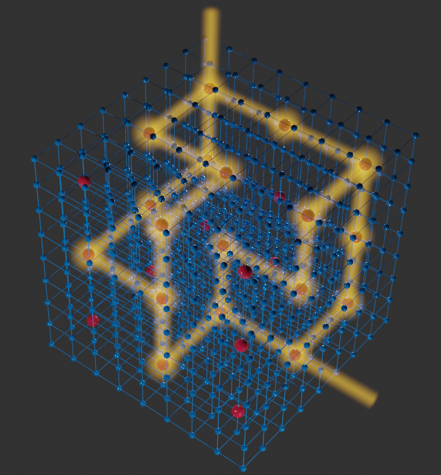
Therefore, we perform in this paper an original experimental study of a 3D photonic band gap cavity superlattice, with a band of photonic states. Metaphorically, we cross the bridge from metamaterial physics to atomic condensed matter physics, using an innovative 3D nanophotonic system: we fabricate 3D photonic crystals with a complete 3D photonic band gap Yablonovitch (1987); John (1987); Joannopoulos et al. (2008) that are doped by judiciously placing resonating cavities in a periodic fashion Hack et al. (2019); Kozoň et al. (2022), see Fig. 1. Since each cavity confines light with a photon energy within the band gap, photons can only propagate by effectively hopping from one cavity to a neighboring cavity on discrete lattice positions in 3D. We observe resonant scattering peaks that match well with theoretical defect bands. When we excite a defect band on resonance, we observe states that spatially extend over multiple superlattice positions . Conversely, if we excite off-resonance, the observed states are localized on single cavity positions. Therefore, light hops in 3D in high-symmetry directions in a crystal, known as Cartesian light, see Fig. 1, which opens avenues to applications in 3D classical and quantum photonic networks Crespi et al. (2016); Hoch et al. (2022); Moughames et al. (2020), and 3D Anderson localization of light Skipetrov and Sokolov (2014).
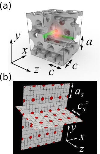
The 3D photonic band gap crystals that we study have a diamond-like inverse woodpile structure Ho et al. (1994) that consist of two arrays of nanopores with radius running in the perpendicular and directions in the high-index silicon backbone 111Each array is rectangular with lattice constants nm and nm. By taking the ratio to be the 3D photonic crystal has a cubic crystal structure that is diamond-like Ho et al. (1994)., as illustrated on YouTube www.youtube.com/nanocops (2012). We employ deep reactive ion etching of silicon through a 3D etch mask on the edge of a long beam Tjerkstra et al. (2011); Grishina et al. (2015); Grishina (2017). Silicon inverse woodpile crystals have a broad and robust 3D photonic band gap Hillebrand et al. (2003); Maldovan and Thomas (2004); Woldering et al. (2009); Adhikary et al. (2020) that is well suited to confine embedded cavities and shield them from the surrounding vacuum. To define a 3D cavity in an inverse woodpile structure, we design two perpendicular and proximal defect nanopores to have smaller radii (see Supplementary) Woldering et al. (2014). Near the intersection of two defect pores, the excess silicon backbone results in a donor-like cavity Joannopoulos et al. (2008). When multiple cavities are spaced periodically in the crystal, coupling between the cavities results in a 3D cavity superlattice that sustains Cartesian light Hack et al. (2019).
We fabricated two types of superlattices with different spacings between the cavities, see Fig. 2 for a scanning electron microscopy (SEM) image of an actual crystal. Since the defect pores are separated by five lattice constants (called SL5), the superlattice has lattice constants in the Y and in the X- and Z-directions. There are defect pores on each crystal surface, hence up to pore crossings and concomitant cavities in the superlattice. We also studied superlattices with lattice spacings and , called SL3, with up to cavities.

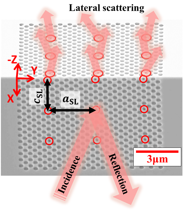
To study the cavity superlattices, we built a confocal microscopy setup (see Supplementary Fig. S3) that simultaneously collects both broadband specular reflectivity to probe the band gap and specular cavity scattering, and lateral scattering by the cavities into non-specular directions, see Fig. 1. Our setup has a frequency range to (or nm) in the near-infrared that is compatible with silicon nanophotonics. The diffraction-limited focus of diameter is smaller than the m distance between neighboring cavities. Therefore, in spatial scans across the superlattice surface, we spatially probe both on and in between the cavities.
Fig. 3 shows representative reflectivity and lateral scattering spectra for two main situations, namely on a cavity (a,c), and in between (b,d) 222In Fig. 3(a) the incident focus is close to the middle defect pore on the XY surface, and in Fig. 3(b) the incident focus is in between the middle and the rightmost defect pore on the XY surface at .. Since the m distance between two cavities is much greater than the Bragg length (m Devashish et al. (2017)), spectra collected in between cavities effectively correspond to probing the unperturbed crystal. In both cases we observe an intense and broad reflectivity peak that corresponds to the 3D band gap of the crystal, see also Ref. Adhikary et al. (2020). While common lore has it that an increased number of defects in a photonic crystal adversely influences a band gap, ultimately even closing it Lidorikis et al. (2000); Li and Zhang (2000); Koenderink et al. (2005), we see here that the introduction of a superlattice of defects does not close the band gap, hence the superlattice modes identified below are indeed confined in a 3D band gap.
To identify reflectivity features in Fig. 3(a), we compare the measurements with the band structures in Fig. 3(c), computed for a cavity superlattice with pore radii corresponding to those obtained at the probing location using the method 333This procedure is necessary since the nanopore radii vary across the sample surface and in depth. Therefore, at every probed location there is effectively a ‘local’ pore radius. In Ref. Adhikary et al. (2020) it is shown that the lower band edge combined with the known gap map Woldering et al. (2009) gives a reliable estimate of the local pore radius from Ref. Adhikary et al. (2020). The band structure shows that the cavity superlattice sustains two types of bands inside the 3D band gap, namely flat defect bands typical of Cartesian light, and other dispersive bands in the upper half of the band gap Kozoň et al. (2022). Due to the appearance of the dispersive bands, the band gap of the cavity superlattice structure shown in Fig. 3(a) is markedly narrower than the unperturbed band gap shown in Fig. 3(b). This is clearly observed in the superlattice spectra, where a broad trough near coincides with the dispersive bands in the upper half of the original band gap, and thus narrows the superlattice band gap 444The modulation of the upper edge of the measured gap versus position is clearly seen in Fig. 5, where the gap narrows at every defect pore and widens in between.. The center frequency and the width of the measured reflectivity band gap of the superlattice (see Figs. 3(a,b)) agree very well with the theoretical band gap (see Figs. 3(c,d), respectively), which highlights that the fabricated nanostructure and its optical functionality match closely with the designed structure and the intended optical behavior. We also observe that upon focusing the incident light on the cavity, the maximum reflectivity (, see Fig. 3(a)) is less than when focusing away from the cavities (, see Fig. 3(b)), which is reasonable since the light incident on cavities is also scattered non-resonantly, thereby reducing the specular reflectivity.
When focusing on a cavity, the lateral scattering spectrum shows a distinct peak at within the band gap, see Fig. 3(a). The peak represents light scattered from incident wave vectors to outgoing wave vectors in completely different directions than either the incident ones or their Bragg diffracted counterparts . Therefore, we expect less light to be reflected and, indeed, the reflectivity spectrum reveals a corresponding trough in the same frequency band. Moreover, the scattering peak and the reflectivity trough match well with a Cartesian superlattice band in the band structures, see Fig. 3(b). We verified that the scattering peak differs from random speckle that is also observed, see S7 in supplementary material. The observation of resonant features both in specular reflectivity and in scattering confirms that the confinement of light in the superlattice is truly a 3D phenomenon, as opposed to 1D confinement in a Fabry-Pérot cavity that would be apparent in reflectivity but not in lateral scattering. We emphasize that the peak only appears when the incident light is focused onto a defect; when the incident light is focused in between defects the peak is absent, see Fig. 3(b)). Hence we conclude that the scattering peak corresponds to a Cartesian superlattice band 555 The sum of the reflectivity and the lateral scattering are less than since our setup can only access part of the light scattered in the -direction into air, whereas light scattered in the -directions escapes undetected. Since these scattered contributions propagate in the high-index Si substrate, it is conceivable that their contributions are considerably larger than the detected fraction in air, that may in turn also be attenuated by Fresnel reflectivity at the crystal-air interface..
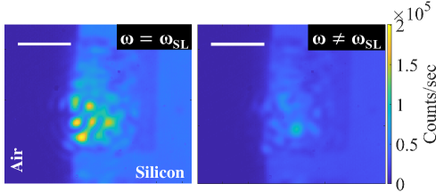
To visualize the hopping of light in the superlattice, we capture images of the front surface of SL3 while varying the frequency. We detect crossed polarized light to suppress single scattering from the sample surface and select light that has multiply scattered inside the crystal. Hence, we expect to detect both light scattered from the cavities and from unavoidable disorder. Fig. 4 presents images for two frequencies , at the center of the superlattice peak (), and away (), within the unperturbed original band gap. In both cases, we see a speckle pattern due to multiple scattering by randomness. A remarkable observation is that at , the light spreads over a large area, much larger than the incident spot. Intensity maxima near the defect pores are observed, as shown in the left image in Fig. 4. In the X-direction, the three intensity maxima are equally spaced, with an average distance of m. This agree very well with the distance between cavities in the X-direction of . The good agreement proves that in SL3, the superlattice frequency hops over at least 3 neighboring cavities, which firmly establishes that we observe light hopping in a 3D superlattice.

Due to an inadvertent nanofabrication inhomogeneity of the underlying band gap crystals, we find from the position-dependent measurement that the band gaps shift across the crystals. Fig. 5(a,b) shows that the band edges shift to lower frequencies while the superlattices are scanned from to m. In superlattice SL5 (Fig. 5(a)), we observe near the 2nd defect pore a scattering resonance centered at . Scanning further to the 3rd defect pore, the scattering resonance is replaced by another one at a lower frequency . Since the peaks differ for the different defects, the cavities are uncoupled in the Y-direction. Strikingly, in superlattice SL3 the scattering peak has the same center frequency () when scanned across multiple cavities, see Fig. 5(b). Therefore, multiple cavities are coupled, hence the peak represents a bona fide superlattice band typical of Cartesian light that hops through the superlattice Hack et al. (2019). To the best of our knowledge, this is the first experimental observation of 3D discretized light transport in a cavity superlattice.
In the pursuit of 3D Anderson localization of light in 3D Skipetrov and Sokolov (2014), it has been suggested that an interesting approach is the analogy with Anderson’s original work Anderson (1958), namely impurities in crystals. If we conceive of cavities as impurities in a photonic band gap, the variation of the individual cavities’ resonance frequency and inter-cavity hopping rates correspond to diagonal and off-diagonal disorder in the Anderson model, respectively.
For future applications as 3D photonic network with potentially more degrees of control than ready-made networks Tajiri et al. (2019), we propose to consider adding phase control to the waves hopping in 3D from cavity to cavity, e.g., by wavefront shaping tools Rotter and Gigan (2017). Hence, light can take a subset of all possible paths (cf. Fig. 1), and thereby, one obtains control on how (which paths) and where (which cavity) the light travels. Since photonic control is nowadays feasible down to single photons Uppu et al. (2020), the notion above could find application in 3D quantum networks with significant network size scaling advantages compared to conventional 2D networks Moughames et al. (2020); Hoch et al. (2022).
Acknowledgments
We thank Cock Harteveld for technical help and sample preparations, Chris Toebes for contributions to the initial experiments, Ad Lagendijk for his valuable feedback, and Arie den Boef, Patrick Tinnemans, Vahid Bastani, Wim Coene, and Scott Middlebrooks (ASML) for helpful discussions. This research is supported by NWO-TTW Perspectief program P15-36 “Free-form scattering optics” (FFSO).
References
- van Haeringen and Lenstra (1990) W. van Haeringen and D. Lenstra, eds., Analogies in Optics and Micro Electronics (Springer, Dordrecht, 1990).
- Soukoulis (2001) C. Soukoulis, ed., Photonic Crystals and Light Localization in the 21st Century (Springer Netherlands, 2001).
- Sheng (2006) P. Sheng, Introduction to Wave Scattering, Localization and Mesoscopic Phenomena (Springer Verlag, 2006).
- Akkermans and Montambaux (2007) E. Akkermans and G. Montambaux, Mesoscopic Physics of Electrons and Photons (Cambridge University Press, 2007).
- Kruglyak et al. (2010) V. V. Kruglyak, S. O. Demokritov, and D. Grundler, Journal of Physics D: Applied Physics 43, 264001 (2010).
- Ghulinyan and Pavesi (2015) M. Ghulinyan and L. Pavesi, Light Localisation and Lasing: Random and Pseudo-random Photonic Structures (Cambridge University Press, 2015).
- Bragg and Williams (1934) W. L. Bragg and E. J. Williams, Proc. Royal Soc. London Series A 145, 699 (1934).
- Bethe (1935) H. A. Bethe, Proc. Royal Soc. London Series A 150, 552 (1935).
- Li et al. (1992) J. Li, M. Chong, J. Zhu, Y. Li, J. Xu, P. Wang, Z. Shang, Z. Yang, R. Zhu, and X. Cao, Applied Physics Letters 60, 2240 (1992).
- Luque and Martí (1997) A. Luque and A. Martí, Physical Review Letters 78, 5014 (1997).
- Tablero et al. (2005) C. Tablero, P. Palacios, J. Fernández, and P. Wahnón, Solar Energy Materials and Solar Cells 87, 323 (2005), international Conference on Physics, Chemistry and Engineering.
- Sullivan et al. (2013) J. T. Sullivan, C. B. Simmons, J. J. Krich, A. J. Akey, D. Recht, M. J. Aziz, and T. Buonassisi, Journal of Applied Physics 114, 103701 (2013).
- Liu et al. (2018) Q. Liu, Z. Cai, D. Han, and S. Chen, Scientific Reports 8, 1604 (2018).
- Yariv et al. (1999) A. Yariv, Y. Xu, R. K. Lee, and A. Scherer, Optics Letters 24, 711 (1999).
- Bayindir et al. (2000) M. Bayindir, B. Temelkuran, and E. Ozbay, Physical Review B 61, R11855 (2000).
- Altug and Vučković (2005) H. Altug and J. Vučković, Optics Express 13, 8819 (2005).
- Ashcroft and Mermin (1976) N. W. Ashcroft and N. D. Mermin, Solid State Physics (Holt, Rinehart and Winston, 1976).
- Hack et al. (2019) S. A. Hack, J. J. W. van der Vegt, and W. L. Vos, Physical Review B 99, 115308 (2019).
- Yablonovitch (1987) E. Yablonovitch, Physical Review Letters 58, 2059 (1987).
- John (1987) S. John, Physical Review Letters 58, 2486 (1987).
- Joannopoulos et al. (2008) J. D. Joannopoulos, S. Johnson, J. N. Winn, and R. D. Meade, Photonic crystals: molding the flow of light (Princeton University, 2008).
- Kozoň et al. (2022) M. Kozoň, A. Lagendijk, M. Schlottbom, J. J. W. van der Vegt, and W. L. Vos, Phys. Rev. Lett. 129, 176401 (2022).
- Crespi et al. (2016) A. Crespi, R. Osellame, R. Ramponi, M. Bentivegna, F. Flamini, N. Spagnolo, N. Viggianiello, L. Innocenti, P. Mataloni, and F. Sciarrino, Nat. Commun. 7, 10469 (2016).
- Hoch et al. (2022) F. Hoch, S. Piacentini, T. Giordani, Z.-N. Tian, M. Iuliano, C. Esposito, A. Camillini, G. Carvacho, F. Ceccarelli, N. Spagnolo, A. Crespi, F. Sciarrino, and R. Osellame, npj Quantum Inf. 8, 55 (2022).
- Moughames et al. (2020) J. Moughames, X. Porte, M. Thiel, G. Ulliac, L. Larger, M. Jacquot, M. Kadic, and D. Brunner, Optica 7, 640 (2020).
- Skipetrov and Sokolov (2014) S. E. Skipetrov and I. M. Sokolov, Phys. Rev. Lett. 112, 023905 (2014).
- Ho et al. (1994) K. M. Ho, C. T. Chan, C. M. Soukoulis, R. Biswas, and M. Sigalas, Solid State Commun. 89, 413 (1994).
- Note (1) Each array is rectangular with lattice constants nm and nm. By taking the ratio to be the 3D photonic crystal has a cubic crystal structure that is diamond-like Ho et al. (1994).
- www.youtube.com/nanocops (2012) www.youtube.com/nanocops, “Animation “3D Photonic Crystal with a Diamond Structure”,” (2012).
- Tjerkstra et al. (2011) R. W. Tjerkstra, L. A. Woldering, J. M. van den Broek, F. Roozeboom, I. D. Setija, and W. L. Vos, J. Vac. Sci. Technol. B 29, 061604 (2011).
- Grishina et al. (2015) D. A. Grishina, C. A. M. Harteveld, L. A. Woldering, and W. L. Vos, Nanotechnology 26, 505302 (2015).
- Grishina (2017) D. A. Grishina, 3D Silicon Nanophotonics, Ph.D. thesis, University of Twente (2017).
- Hillebrand et al. (2003) R. Hillebrand, S. Senz, W. Hergert, and U. Gösele, Journal of Applied Physics 94, 2758 (2003), https://doi.org/10.1063/1.1593796 .
- Maldovan and Thomas (2004) M. Maldovan and E. L. Thomas, Nature Materials 3, 593–600 (2004).
- Woldering et al. (2009) L. A. Woldering, A. P. Mosk, R. W. Tjerkstra, and W. L. Vos, J. Appl. Phys. 105, 093108 (2009).
- Adhikary et al. (2020) M. Adhikary, R. Uppu, C. A. M. Harteveld, D. A. Grishina, and W. L. Vos, Optics Express 28, 2683 (2020).
- Woldering et al. (2014) L. A. Woldering, A. P. Mosk, and W. L. Vos, Physical Review B 90, 115140 (2014).
- Note (2) In Fig. 3(a) the incident focus is close to the middle defect pore on the XY surface, and in Fig. 3(b) the incident focus is in between the middle and the rightmost defect pore on the XY surface at .
- Devashish et al. (2017) D. Devashish, S. B. Hasan, J. J. W. van der Vegt, and W. L. Vos, Physical Review B 95, 155141 (2017).
- Lidorikis et al. (2000) E. Lidorikis, M. M. Sigalas, E. N. Economou, and C. M. Soukoulis, Phys. Rev. B 61, 13458 (2000).
- Li and Zhang (2000) Z.-Y. Li and Z.-Q. Zhang, Physical Review B 62, 1516 (2000).
- Koenderink et al. (2005) A. F. Koenderink, A. Lagendijk, and W. L. Vos, Physical Review B 72, 153102 (2005).
- Note (3) This procedure is necessary since the nanopore radii vary across the sample surface and in depth. Therefore, at every probed location there is effectively a ‘local’ pore radius. In Ref. Adhikary et al. (2020) it is shown that the lower band edge combined with the known gap map Woldering et al. (2009) gives a reliable estimate of the local pore radius.
- Note (4) The modulation of the upper edge of the measured gap versus position is clearly seen in Fig. 5, where the gap narrows at every defect pore and widens in between.
- Note (5) The sum of the reflectivity and the lateral scattering are less than since our setup can only access part of the light scattered in the -direction into air, whereas light scattered in the -directions escapes undetected. Since these scattered contributions propagate in the high-index Si substrate, it is conceivable that their contributions are considerably larger than the detected fraction in air, that may in turn also be attenuated by Fresnel reflectivity at the crystal-air interface.
- Anderson (1958) P. W. Anderson, Physical Review 109, 1492 (1958).
- Tajiri et al. (2019) T. Tajiri, S. Takahashi, Y. Ota, K. Watanabe, S. Iwamoto, and Y. Arakawa, Optica 6, 296 (2019).
- Rotter and Gigan (2017) S. Rotter and S. Gigan, Rev. Mod. Phys. 89, 015005 (2017).
- Uppu et al. (2020) R. Uppu, F. T. Pedersen, Y. Wang, C. T. Olesen, C. Papon, X. Zhou, L. Midolo, S. Scholz, A. D. Wieck, A. Ludwig, and P. Lodahl, Sci. Adv. 6, eabc8268 (2020).
- Setyawan and Curtarolo (2010) W. Setyawan and S. Curtarolo, Comput. Mater. Sci. 49, 299 (2010).
- Johnson and Joannopoulos (2001) S. Johnson and J. Joannopoulos, Optics Express 8, 173 (2001).
- Thijssen et al. (1999) M. S. Thijssen, R. Sprik, J. E. G. J. Wijnhoven, M. Megens, T. Narayanan, A. Lagendijk, and W. L. Vos, Physical Review Letters 83, 2730 (1999).
- Ctistis et al. (2010) G. Ctistis, A. Hartsuiker, E. van der Pol, J. Claudon, W. L. Vos, and J. M. Gérard, Physical Review B 82, 195330 (2010).
- Huisman et al. (2011) S. R. Huisman, R. V. Nair, L. A. Woldering, M. D. Leistikow, A. P. Mosk, and W. L. Vos, Physical Review B 83, 205313 (2011).
- Note (6) For spectral measurements the SLM is used to reflect as a mirror. In addition, the SLM is also used to correct a tilted beam in the setup as explained in the Appendix of this chapter.
- (56) I. I. (Petersburg), “Semiconductors,” http://www.ioffe.ru/SVA/NSM/Semicond/.
- Note (7) The Si reflectivity spectrum has a small positive slope with frequency since we do not consider the change of refractive index with frequency within this range.
- Goodman (2007) J. Goodman, Speckle Phenomena in Optics: Theory and Applications (Roberts & Company, 2007).
- Dainty (2013) J. Dainty, Laser Speckle and Related Phenomena, Topics in Applied Physics (Springer, Berlin Heidelberg, 2013).
Observation of light propagation through a three-dimensional cavity superlattice in a 3D photonic band gap
(Supplementary Material)
Manashee Adhikary
Marek Kozoň
Ravitej Uppu
Willem L. Vos
In this Supplementary, we provide more details on the structure of the inverse woodpile crystals, on the definition of the cavities. We describe the optical setup in detail, as well as a number of experimental procedures. We show additional experimental results, notably the reproducibility of the lateral scattering to distinguish superlattice peaks from random speckle.
.1 Inverse woodpile photonic crystals and cavity design
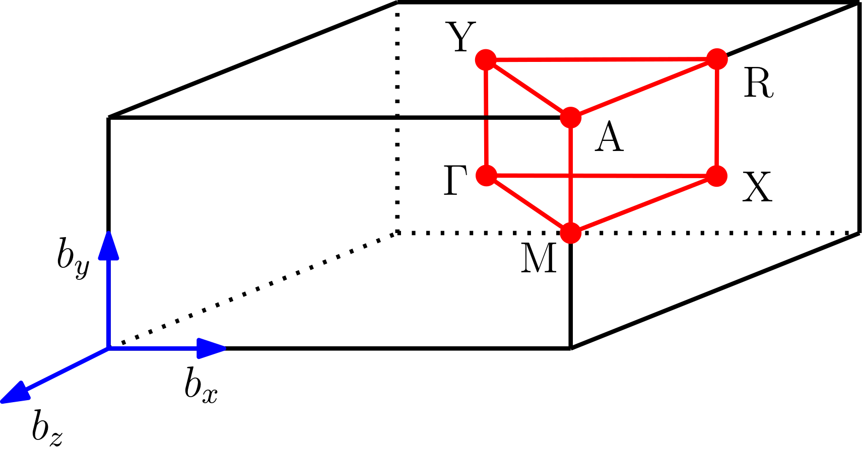
To create a resonant cavity in an inverse woodpile photonic crystal, Woldering et al. proposed a design whereby two proximal perpendicular pores have a smaller radius than all other pores, as shown in Fig. S1(a) Woldering et al. (2014). This structure has a tetragonal crystal symmetry, with the Brillouin zone and its high-symmetry path depicted in Fig. S2. Near the intersection region of the two smaller pores, the light is confined in all three directions to within a mode volume as small as where is the free-space wavelength Woldering et al. (2014). Supercell band structures reveal up to five resonances within the band gap of the perfect crystal, depending on the defect pore radius Woldering et al. (2014). The best confinement occurs for a defect radius that is also considered here.
Fig. S1(b) shows a 3D superlattice of cavities as is studied here, where each sphere indicates one cavity, as shown in Fig. S1(a). The cavity superlattice has lattice parameters (, , ) in the () directions that are integer multiples of the underlying inverse woodpile lattice parameters: , , . Here, we study the superlattice such that the cavities are repeated every three unit cells with lattice parameters , , . Thus, the cavity superlattice is also cubic, similar to the underlying inverse woodpile structure.
We have calculated the band structure of the 3D cavity superlattice using the plane-wave expansion method Ashcroft and Mermin (1976); Joannopoulos et al. (2008), implemented in the recent version 1.5 of the MIT photonic bands (MPB) code Johnson and Joannopoulos (2001). We employ the grid resolution per unit cell of the superlattice. All calculations were performed on the “Serendipity” cluster in the MACS group at the MESA+ Institute.
.2 Optical setup
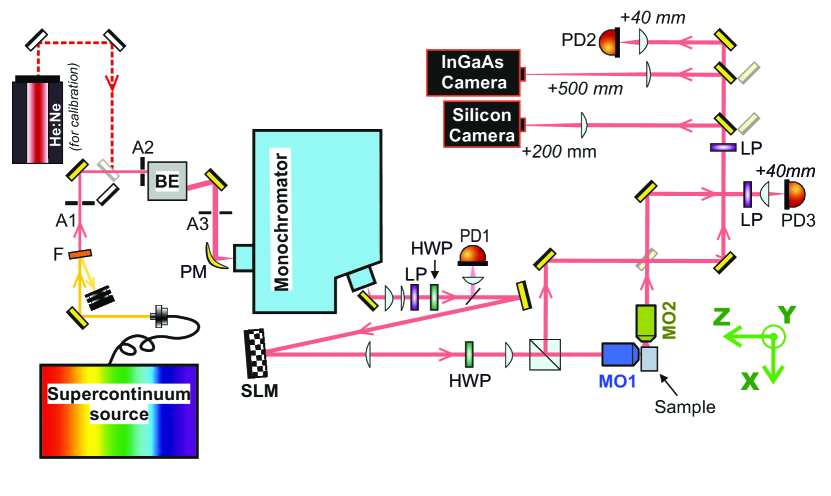
We have developed a versatile near-infrared setup to collect position-resolved broadband reflectivity and lateral scattering spectra of photonic nanostructures, as well as to perform wavefront shaping to focus light inside samples. All measurements are processed in LabView environments. The near-infrared range of operation is compatible with 3D silicon nanophotonics as it avoids intrinsic silicon absorption. A pictorial representation of the full optical setup is shown in Fig. S3. The setup consists of three main components:
-
1.
a broadband tunable coherent source,
-
2.
a broadband wavefront shaper, and
-
3.
twin-arm imaging of reflected and lateral (YZ-plane) scattered signals from the sample.
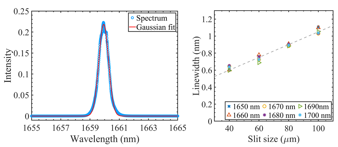
The reflectivity part has been described earlier in Ref. Adhikary et al. (2020). The broadband tunable coherent source is realized by spectrally filtering the emission from a supercontinuum source (Fianium SC 450-4, 450 - 2400 nm) with a monochromator (Oriel MS257; 1200 lines/mm grating). A long-pass filter (cut-off wavelength 850 nm) is used to reject the background from second-order diffraction of shorter wavelengths. The filter is slightly tilted so that reflected light does not go back into the collimator and source (where it could lead to unwanted feedback and damage to the source), but gets absorbed in a beam dump. The filtered light beam is expanded in a reflecting beam expander (Thorlabs) and sent to a parabolic mirror (PM) to focus the light to fit through the input slit of the monochromator. The monochromator scans optical frequencies ranging from to (or wavelengths nm) with a linewidth of nm exiting from the output slit of width m (see Fig. S4), and a tuning precision better than nm. Since we use this setup also for wavefront shaping, we use sequential scanning of wavelengths instead of measuring the spectrum at once with a spectrometer as in Thijssen et al. (1999); Ctistis et al. (2010); Huisman et al. (2011). A He:Ne laser is used to calibrate the grating of the monochromator, and is not used for measurements. The filtered light is then collimated and expanded to a beam diameter of mm. A small fraction () of the light is sent to a photodiode PD1 using a glass plate as a reference to monitor the input power. The main beam is incident on a reflective phase-only spatial light modulator (Meadowlark optics; pixels; AR coated: nm). Since the output of the source is randomly polarized, a linear polarizer (LP) followed by a half-wave plate (HWP) are placed at the monochromator output to select the desired linear polarization orientation, since the polarization has to be parallel to the slow axis (in this case the Y-axis of the SLM) for the SLM to optimally function. At this point, the setup is described in detail first from the point of view of spectroscopy and next wavefront shaping.
.3 Near-infrared reflectivity and lateral scattering
In our optical setup shown in Fig. S3, the sample is mounted on an XYZ translation stage that has a step size of about nm. The reflected light from the SLM 666For spectral measurements the SLM is used to reflect as a mirror. In addition, the SLM is also used to correct a tilted beam in the setup as explained in the Appendix of this chapter. is sent to an infrared apochromatic objective (Olympus LC Plan N 100) to focus the light onto the sample’s surface with a numerical aperture NA . The beam waist of the light reflected from the SLM is narrowed and re-collimated by a pair of lenses so that it fits the back aperture of the objective. The diffraction limit in the setup is about m at longer wavelengths. A second HWP is introduced on the beam path before the objective to rotate the linear polarization of the incident light on the sample for polarization-dependent measurements.
Light reflected by the sample is collected by the same objective and a beam splitter directs the reflected light towards the detection arm where the reflection from the sample is imaged onto an IR camera (Photonic Science InGaAs). In order to locate the focus of the input light on the surface, a NIR LED is used to illuminate the sample surface. We use the XYZ translation stage to move the sample to focus the light on the desired location. For example, an image of a 3D crystal as seen on the IR camera reveals the surface of the Si beam, see for example Fig. 4 in the main manuscript. The bright circular spot with a diameter of about 2 m is the focus of light reflected from the crystal. The rectangular darker areas of about 8 m 10 m are the XY surfaces of the 3D photonic crystals. They appear dark compared to the surrounding silicon since the LED illumination is outside the band gap of these crystals whose effective refractive index is less than that of silicon.
Once the input light beam is focused on the sample, the reflected light is sent to photodiode PD2 (Thorlabs InGaAs DET10D/M, 900 nm - 2600 nm) by flipping out the mirror in front of the camera. The photodiode records the reflected intensity as the monochromator scans the selected wavelength range. At the same time, the scattered light from the sample in the lateral direction is collected by a long working distance apochromatic objective MO2 (NA = ), and sent to a third photodiode PD3 (similar to PD2). An analyzer in front of each photodiode is used to select either parallel or cross polarization of the reflected and scattered light with respect to the input. Thus, in total we get two sets of spectra as signal every time the wavelengths are scanned through the desired range: a reflectivity spectrum, and a lateral scattering spectrum. By moving the sample stage in the -direction, the focus is scanned across the crystals with a step size of , resulting in typically reflectivity and lateral scattering spectra per scan.

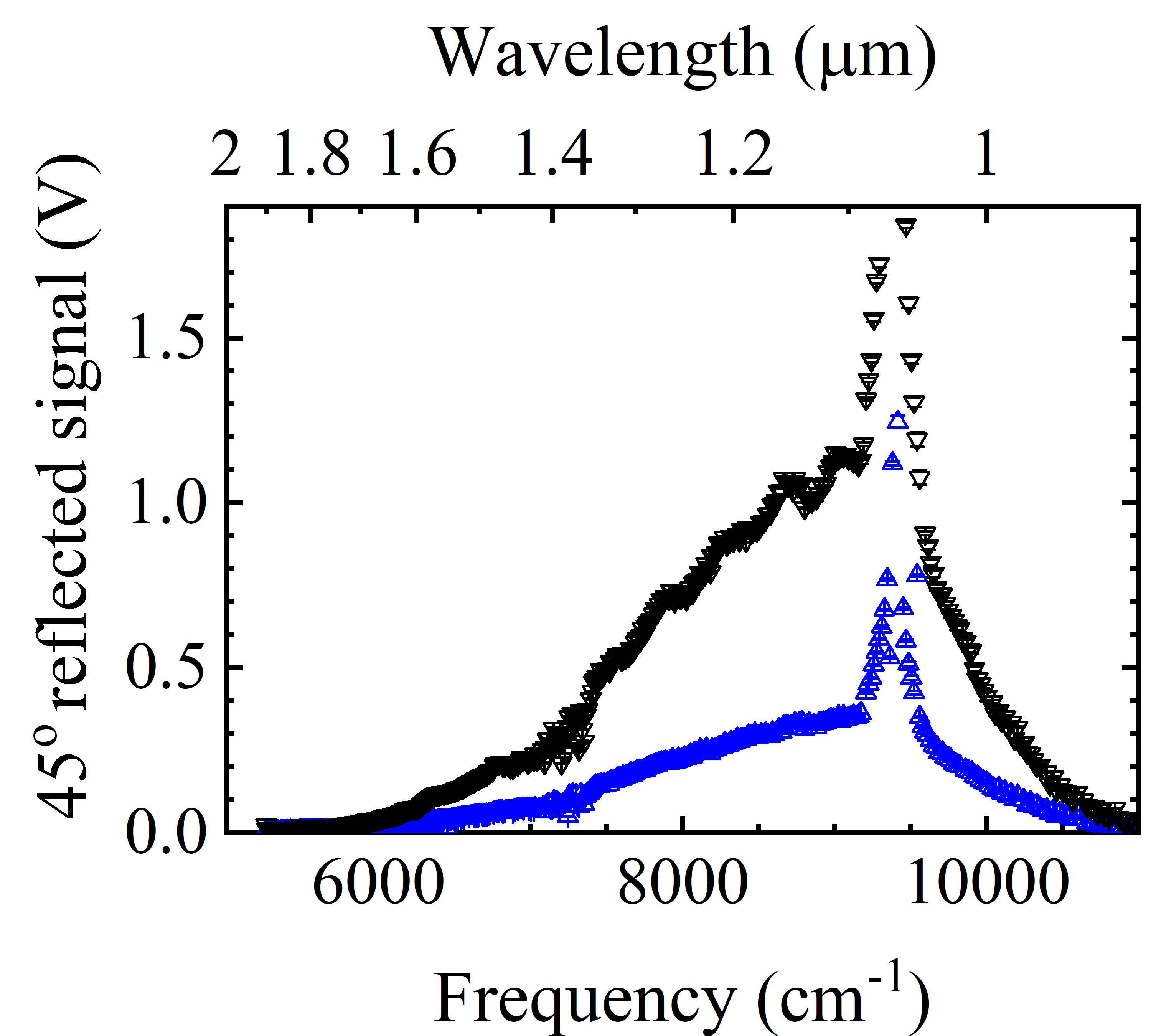
The raw reflectivity measured on two reference samples, viz., a clean gold mirror and the bulk silicon substrate are shown in Fig. S5(a). The spectra show that the intensity of the supercontinuum source varies markedly with frequency, hence proper referencing is important. The intensity cut-off at high frequencies is mainly due to limited detection bandwidth of the InGaAs photodiode and the cut-off at low frequencies is due to the absorption by the refractive optics (lenses, objectives, wave plates) and the limited bandwidth of the supercontinuum source. The range of noisy data near is attributed to water vapor absorption that may vary from day-to-day depending on lab conditions (and weather). Hence care is exerted while analyzing data in this wavelength range, by using data obtained in a narrow time window. In future, the noise may be suppressed by placing the setup in box purged with dry air or nitrogen. The intense peak at 1064 nm is the pump wavelength of the supercontinuum source; due to unavoidable detector saturation near this peak, data in this range is typically removed from analysis. Recording a typical reflectivity or lateral scattering spectrum takes about 5 to 25 minutes, depending on the chosen wavelength step size (typically 10 nm or 2 nm). The calibrated reflectivity and lateral scattering are defined as
| (S1) | |||
| (S2) |
For reflectivity, the spectral response of the samples is referenced to the signal reflected from a clean gold mirror that reflects . Since it is tedious to dismount and realign the sample to take reference spectra during long measurements on crystals on a silicon beam, we also take secondary reference measurements on bulk silicon outside the crystals, which has a flat response with respect to the gold mirror. The bulk silicon reflectivity is plotted in Fig. S5(b) that agrees with the expected reflectivity of Si for normal incidence in the NIR spectral region () (Petersburg). The spectrum is flat 777The Si reflectivity spectrum has a small positive slope with frequency since we do not consider the change of refractive index with frequency within this range. without any features apart from the noisy data mentioned above. Therefore, we use the Si signal also as a reference for reflectivity measurements.
The reference for lateral scattering is a bit tricky since we need to have the input signal go through the objective MO2 for correct referencing. Therefore we used the edge of a silicon beam that was cut at to reflect the incoming light coming through MO1 towards MO2 and send it to PD3, just like the lateral scattering signal. Using Fresnel reflectivity of incident light on silicon, we use a calibration of reflectivity for -polarized light and reflectivity for -polarized light. To ensure that the signal to noise ratio of the photodiode response is sufficient to detect signal in the desired range, each detector photodiodes are fed into a lock-in amplifier to amplify the signal with a suitable gain. Since a serial measurement mode holds the risk of possible temporal variations in the supercontinuum source, we simultaneously collect the output of the monochromator with photodiode PD1 in each reflectivity scan. An example of reference spectra for LS measurements is shown in Fig. S6 for two orthogonal polarizations of the incident light. All measurements described above are controlled by and the data saved by a home-built LabVIEW program, that also allowed for remote control, which turned out to be very convenient when access to our laboratories was restricted during the Covid pandemic.
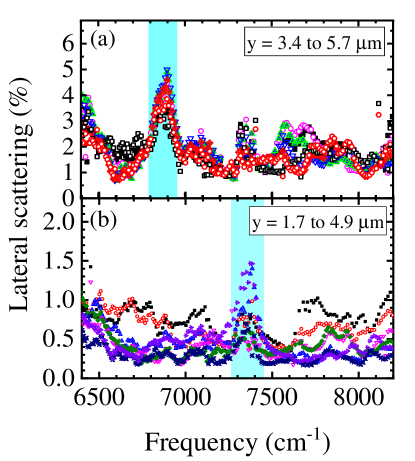
.4 Distinguishing superlattice scattering from random speckle
To distinguish a superlattice peak from random speckle peaks Goodman (2007); Dainty (2013) that arise as a result of random and unavoidable structural variations Koenderink et al. (2005), we monitor the reproducibility of the peaks while scanning the illuminating spot across the sample surface. Therefore, we plot multiple lateral scattering spectra at different -positions near the defect pore (at m), as shown in Fig. S7(a) and (b) for the superlattices SL5 and SL3, respectively. It is clearly apparent that the peak near reproduces at all positions near the defect pore, with gradually decreasing intensity as the focus moves away from the defect pore. We also observe a second reproducing peak near , possibly a second superlattice band. For superlattice SL3 (Fig. S7(b)), we also see a scattering peak near that reproduces even across multiple defect pores. All other scattering peaks do not reproduce, hence they are uncorrelated speckle arising from unavoidable disorder of the crystal. Therefore, we conclude that all reproducing peaks are spectral features of the intentional superlattice of defects.