Two Anderson impurities coupled through a superconducting island: charge stability diagrams and double impurity qubit
Abstract
We present a model of two Anderson impurities coupled to and through a superconducting island. The model parametrizes the strength of the coupling between impurity sites, allowing it to represent a variable distance between the impurities. We systematically explore the effect of the model parameters in the subspaces with total even and odd occupancy, identifying unique features of the charge stability diagrams that distinguish the two parities.
For total odd electron parity, we identify a device tuning, in which the splitting between the two lowest energy states is highly insensitive to changes of the chemical potentials. We investigate the degree to which a qubit based on such two states is tunable and discuss an optimal choice of parameters to maximize inhomogeneous dephasing time. Finally, we point out that the proposed qubit lacks a transition dipole moment, and outline some of the consequences on viable driving and readout mechanisms. The prototype qubits could be realized with the existing capabilities of coupling quantum dots to hard-gapped superconductors.
I Introduction
The prerequisite to designing a well-performing qubit was to make it highly insensitive to environmental charge noise. Superconducting qubit designs, such as transmons [1] and fluxonium [2], achieve this by using, respectively, large capacitance and large inductance to shunt two superconducting islands. Spin qubits achieve charge-noise insensitivity by relying on a degree of freedom that is (at least in principle) independent of charge [3]. Last but not least, proposals such as [4] and Majorana qubits [5], aim to use topological protection to pin the qubit states at zero energy.
Hybrid approaches, which combine superconducting and semiconducting materials, have demonstrated the capacity for coherent manipulation [6, 7, 8], including two-qubit coupling [9]. However, their performance to date is not sufficient to approach the fidelity thresholds required for quantum error correction. Nevertheless, hybrid structures turned out to be a platform suitable for investigating an extraordinary range of physical phenomena, including but not limited to the multiterminal Josephson effect [10, 11], superconductor-insulator transition [12] and (signatures of) topological superconductivity [13, 14, 15, 16, 17].
A commonly recurring component of super-semiconducting structures is a discrete Fermionic state (e.g. a quantum dot), tunnel coupled to a bulk or mesoscopic superconductor [18, 19]. Such a component introduces a subgap state into the excitation spectrum, referred to in the literature as Shiba, Yu-Shiba-Rusinov, or Andreev bound state, depending on the device parameters [20]. Subgap states can abruptly switch between singlet and doublet ground states (characterized by different total electron parity) under tuning of chemical potential, magnetic field, and so on, constituting a canonical example of a quantum phase transition. The subgap states are studied by their influence on the spectrum of the Josephson junction [21, 22, 23, 24, 25] and can be combined into chains and molecules [26, 27, 28, 29, 30].
In this paper, we describe a system consisting of two Anderson impurities coupled to and through a common superconductor. We enforce the fixed charge on the superconductor and impurities as a whole, which corresponds to the electrostatic floating of the device. Such a configuration prevents conventional transport measurements, and therefore we study the occupancy and quantum capacitance related to the electron tunneling between the impurities and the island. In particular, we identify the differences between the charge stability diagrams with different total electron parities and identify the charge transitions enabling the on-demand generation of entangled spins via Cooper pair splitting.
For total odd electron parity, we identify a device tuning in which the splitting between the two lowest-energy states is highly insensitive to changes of the chemical potential of the impurities. Such insensitivity indicates a potential for the realization of a qubit highly insensitive to charge noise. We investigate the degree to which such a qubit is tunable and discuss an optimal choice of parameters to maximize inhomogeneous dephasing time. Finally, we point out that the proposed qubit lacks a transition dipole moment, and outline some of the consequences on viable driving and readout mechanisms.
We structure the discussion by dividing the article into three main sections. In section II we introduce the model used to simulate the two impurities coupled to a superconducting island. Section III systematically analyzes the system: first, removing all coupling terms, and gradually reintroducing them to emphasize effects related to the total parity. Having explored the model, in Sec. IV we focus on a specific device configuration, identify the low-energy subspace we propose to use as a qubit, and explore its tunability, possible performance, and some consequences of the vanishing transition dipole moment.
II The system Hamiltonian in BCS zero bandwidth approximation
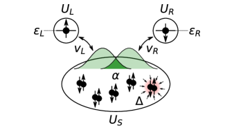
We start by introducing the effective Hamiltonian of Anderson’s impurity in the zero-bandwidth BCS approximation, where the superconductor is described as orbitals with a mean-field pairing interaction [31]. The left and right impurity sites () correspond to the Fermionic creation operators , with , and the corresponding electron number operators are denoted as .
The superconductor is represented by two orthogonal orbitals (where ), each with the pairing term . The impurity sites are coupled to the superconductor through a term . We achieve a variable overlap between impurities by choosing and . The transformation is intentionally non-unitary, so that represents an effective distance between the impurity sites. The limit represents the distance between the impurity sites much greater than the coherence length of the superconductor, and, conversely, represents the two impurities coupled to the superconductor exactly at the same place.
In summary, we describe the system using a Hamiltonian.
| (1) | ||||
The first row of the Hamiltonian describes the tunable chemical potential of the impurities and their charging energy . The second row represents the charging energy of the superconducting island . Since the total charge is fixed, the charge on the island is expressed in terms of the occupancy of the impurity sites . The third row represents the coupling of the impurity sites to the superconductor . The last row represents the superconducting coupling at the two superconducting orbitals .
To illustrate the experimental relevance of the proposal, in the following sections we employ parameter values relevant for a specific platform – the semiconducting quantum dots in 2-dimensional electron or hole gas, and the superconducting island is based on an aluminum-proximitized semiconductor. Such a choice sets the Hamiltonian parameters to the typical values of about:
-
•
from 0.05 to 5 meV;
-
•
from 0 to 5 meV;
-
•
from 0.2 to 0.3 meV.
In the remainder of the paper, we set meV and vary other parameters.
III Charge stability diagrams
III.1 Stability diagrams in absence of tunnel coupling
We begin by investigating the interplay between the superconducting gap and the charging energies while setting and . Fig. 2) presents the resulting charge stability diagrams, and the ground state charge dependence on the chemical potential of the left and the right dot .
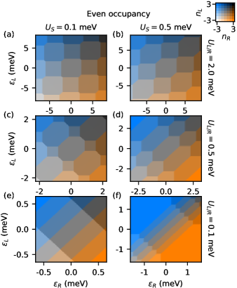
For (Fig. 2(a)) the charge stability regions form a near-square lattice. Vertical (horizontal) charge transitions correspond to moving a single electron between a superconducting island and a right (left) dot. The charge stability regions with an even number of electrons on the island are slightly increased in size, due to the energy reduced by .
As the value of decreases, the term becomes increasingly more relevant, leading to the shrinking and eventual disappearance of the stability regions with an odd-occupied island (Fig. 2(c,e)). On the other hand, increasing has the effect of stretching the charge stability regions along the axis (Fig. 2(b,d,f)).
In the absence of tunnel coupling terms, neglecting the level spacing in the dots results in identical charge stability diagrams for total even and odd total occupancies. The only difference is that the centers of charge stability regions with even- and odd-occupied island exchange positions. The exchange of positions, as well as a set of charge stability diagrams for a larger set of and values, is presented in Supplementary FIg. LABEL:fig_no_tunneling_overview. Now, we fix meV and meV. For these values, both the even and odd charge stability regions are sizable and easily distinguishable, allowing us to illustrate the consequence of nonzero tunnel couplings and , as well as .
III.2 Impurity-island coupling in total even and odd occupancy
Non-zero tunnel couplings predominantly affect the vicinity of the charge transitions, which motivates us to change the focus to the quantum capacitance of the left and the right impurity with respect to the gate voltage that controls its chemical potential . Including the thermal distribution between the eigenstates of the Hamiltonian, the quantum capacitance is given by [32, 33]
| (2) |
where is the canonical partition function, is the energy of the -th lowest state, eV represents the temperature ( mK), and the lever arms are set to .
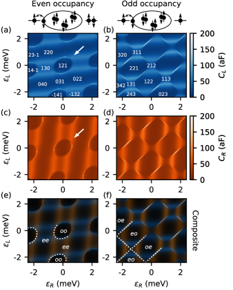
We set a moderately high value of the impurity-island coupling meV and keep zero overlap between the impurity wavefunctions . The resulting charge stability diagrams (Fig. 3) exhibit a striking difference depending on total parity. In the total even occupancy some of the transitions are broadened, nearly merging the two neighboring charge states. Other charge states (indicated by arrows in Fig. 3(a,c), and outlined with dotted lines in (e)) remain sharply separated, rounded in shape, and shrink in their extent.
Differently, in the total odd occupancy, all of the transitions that exchange an electron between one of the dots and the island are broadened, and none of the stability region shapes is rounded. The diagonal two-electron transition (with positive and negative slopes) is sharp and divides the gate voltage space into rectangles (as outlined with dotted lines in Fig. 3(f)). Supplementary Fig. LABEL:fig_symmetric_tunneling_overview illustrates that the differences between the total oven and odd occupancy are not a consequence of fine-tuning, but develop gradually as the tunnel coupling increases.
The sharp charge transitions indicated in Fig. 3(f) originate from the separation of the Hilbert space into two subspaces, differing in the parity of the impurity sites. The ground state always consists of a doublet localized on one impurity and a singlet on another ( and ), but these subspaces do not couple due to the lack of crossed Andreev reflection and cotunneling through the island ().
For even total occupancy (Fig. 3(e)), the rounded region () corresponds to the 4-degenerate ground state with both impurities in a doublet state. In the surrounding area () both impurities are in a singlet state, with all electrons paired on an island, impurity, or on a formed subgap states.
III.3 Overlap of impurity wavefunctions
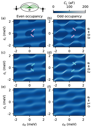
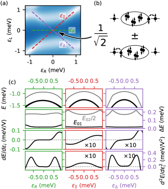
To complete the exploration of the charge stability diagrams, we add an overlap between the electronic wavefunctions localized at the two impurity sites. Increasing the value of from 0 to 0.2 and 1 (Fig. 4) allows tunneling of the quasiparticle between the two impurity sites. In the total even occupancy, this introduces coupling between and subspaces, and in the total odd occupancy, between and subspaces (c.f. Fig. 3(e,f)). Increasing from 0 to 0.2 creates an avoided crossing between those subspaces, prevents thermal excitations, and allows the detection of the quantum capacitance of the ground state [32]. As a result, the corresponding charge transitions broaden, and the measured capacitance increases in magnitude. A further increase in broadens the charge transitions even more but reduces the capacitance magnitude.
In the charge stability diagrams, we highlight transitions of interest, indicated with colored line segments. The corresponding energy diagrams are shown in Fig. 5. The transitions indicated by the negative diagonal line segments in Fig. 4 correspond to elastic cotunneling of a single quasiparticle between left and right impurities (Fig. 5(a,b)). In these cases, the energy diagram is analogous to that of a normal double quantum dot with direct tunnel coupling [34], or coupling via an intermediate quantum state [35].
For total even occupancy, the ground state is a non-degenerate spin singlet, and the lowest excited state is a triply degenerate spin triplet. The splitting between the singlet and triplet subspaces is minimized in the charge stability region, where the wavefunctions of the two odd occupied impurities overlap the least and are maximized in the charge stability region, where the spin tripled state is in Pauli spin blockade, analogous to a conventional double quantum dot. In contrast, in total odd occupancy, the doubly spin-degenerate undergo avoided crossing at between and charge stability regions without spin blockade taking place.
The transitions along positive diagonal line segments in Fig. 4(a-d) correspond to the splitting of the Cooper pair into two quasiparticles. The corresponding energy diagrams (Fig. 5(c,d)) have an identical structure to the co-tunneling transitions (Fig. 5(a,b). The identical structure of the energy diagrams suggests a concrete realization of the on-demand cooper splitting by the adiabatic crossing of the charge transition with a baseband pulse tuning the chemical potential of the two impurities simultaneously. Such a protocol requires only the means of tuning the chemical potential, such as those in Ref. [34]. The protocol was hinted at in Ref. [36] and is likely to be possible to execute in setups exhibiting high efficiency of Cooper pair splitting [37, 38]. However, the direct Bell test on the ejected spin would require implementation in a material that enables high-fidelity single-spin rotations and single-shot readout.
IV The double-impurity qubit
For a total-odd occupancy, a point of particular interest lies at the crossing of dotted-white lines. In the remainder of this article, we present that in the absence of subgap state overlap, the degeneracy between the and states enjoys a high degree of protection from the charge noise. Building on that observation and reintroducing the wavefunction overlap, we propose a qubit realization based on the location of the quasiparticle that can enjoy near third-order protection against charge noise.
IV.1 A sweet spot with near-third order protection
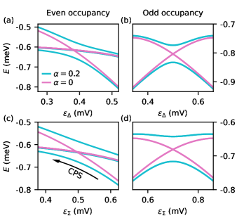
We proceed to identify a point in the charge stability diagram for a total odd electron occupancy where the splitting between the two lowest-energy states exhibits exceptionally weak dependence on the chemical potentials. Such a point would mark a potential for implementation of a qubit with a relatively long coherence time. The promising sweet spot lies at the intersection of positive and negative diagonal lines that separate the ground state and (cf. Fig. 3(f)). Fig. 6 presents the charge stability diagram in the vicinity of the sweet spot. We dedicate this section to the analysis of its properties and tunability.
The two lowest eigenstates at the sweet spot are, illustratively, equal superpositions of and , where the three indices represent the occupancy of the left dot, island, and the right dot (up to ; indicates a spin of a singly occupied dot). The two states correspond to a single quasiparticle occupying one of the two impurity sites, similar to an electron in the case of a charge qubit, or a Cooper pair in the case of a Cooper pair box qubit. A critical feature that distinguishes the proposed sweet spot is the introduction of the superconducting island. The electron-hole symmetry introduced by the island suppresses the charge dispersion, in the sense that for , , and any superposition of these states.
The top row in Fig. 6(c) presents an energy diagram of the three lowest states, the qubit, and the lowest non-computational state, with respect to , and for meV, mV, meV, meV and . The second row illustrates that the qubit splitting (black) is minimal at the sweet spot ( eV; GHz) and over an order of magnitude smaller than the energy of the lowest non-computational state ( eV, GHz). Due to left-right and electron-hole symmetries, the splitting at the sweet spot is first-order insensitive to the chemical potential of the dots individually, as well as to their difference and common mode, as illustrated in the third row by depicting the derivatives of the qubit splitting with respect to 111 The derivatives are to be understood as taken along the axis illustrated in Fig. 6, that is, with , and . . The notable feature of the qubit is that the second derivative of qubit splitting with respect to gate voltages is also exceptionally small. This is in contrast to charge qubits and Cooper pair box qubits, characterized by very short coherence times, for which the second derivative is maximized at the first-order sweet spot.
We propose that the nearly third-order insensitivity to chemical potential makes and states promising for the realization of a highly coherent qubit, and the charge protection is qualitatively different from that for superconducting, spin, and topological qubits. Next, quantify the possible coherence time of the qubit in the presence of quasistatic noise and investigate the optimal choice of , , and .
IV.2 Qubit tunability in microwave frequency range
A realization of the DIQ would consist of dots or impurities of a fixed charging energy at a fixed distance. Thereby we address the question, for fixed and , is it always possible to tune the qubit to arbitrary energy (frequency) within the range conveniently accessible by microwave driving?
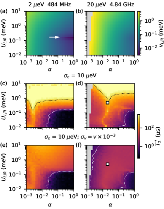
As an example, we select representative qubit splittings of and 20 eV, corresponding to the frequencies of MHz and 4.84 GHz, respectively. Figure 7(a,b) presents the values of required to tune those qubit frequencies for a range of and values and for fixed meV, meV. The values of and for which tuning to the desired frequency requires meV are indicated in gray.
In general, the reduced overlap of superconducting orbitals requires compensation by increasing . The only qubit configuration that is not accessible with a constraint meV is the large qubit splitting for the smallest values of alpha . We do not expect that to be an obstacle since we demonstrate further that this regime is not optimal for maximizing the inhomogeneous dephasing time.
Otherwise smooth map of the values has one characteristic feature, for 2 eV qubit splitting, indicated by a white arrow in Fig. 7(a). This feature corresponds to meV and indicates the particularly small values of required to induce qubit splitting.
A particular value of meV corresponds to . In the absence of tunnel couplings, such a choice of parameters would lead to the degeneracy between even- and odd-occupied islands, namely the exact values of at which the smaller stability regions, as in Fig. 2, have shrunk to zero sizes.
IV.3 Pure dephasing due to charge noise
Now, we illustrate the degree of impact of charge insensitivity on the DIQ performance. In the analysis, as a figure of merit, we choose an inhomogeneous dephasing time under the influence of quasistatic noise.
First, we consider exclusively quasistatic noise that independently affects the chemical potential of the impurities, characterized by a Gaussian distribution with an RMS magnitude of eV. The magnitude of the noise is chosen according to the experimental results on gate-defined spin-qubits [40, 41]. Although the assumed noise is Gaussian, it couples to the qubit frequency via a highly nonlinear dependence. Thus, we expect the Ramsey decay to be characterized by an envelope very different from the usual functional form of . Therefore, we sample 500 values of the qubit frequency around the qubit sweet spot. We identify as the time scale at which the Ramsey oscillations decay by a factor of .
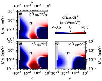
Figure 7(c,d) presents the maps of for the qubit tuned to the splitting of 2 and 20 eV and suggests the most optimal and most ill-advised parameter choices. The unfavorable tuning is the regime of small and large , appearing as a dark region in the bottom right of the color maps. In that regime, the unpaired quasiparticle is strongly localized on the impurity sites. The quasiparticle orbitals on the superconductor have high energy and only mediate the co-tunneling and crossed Andreev reflection through virtual tunneling. As a consequence, qubit splitting and its second derivatives have local extrema at the sweet spot. We illustrate this in Fig. 8, which plots the second derivatives at the sweet spot for eV. The presence of the local extrema is similar to a charge and Cooper pair box qubits and leads to the estimated dephasing times s.
Reducing while increasing , for small eV, increases the coherence time. In particular in a range of values we estimate s (bright vertical feature at about and 0.02 in Fig. 7(c,d)). Compared to Fig. 8, we identify the region of increased coherence with reduced second derivatives of the qubit splitting. A square marker points to an approximate choice of the parameters in Fig. 6.
Increasing leads to a further increase in the estimated , over 1 ms. Accordingly, the second derivatives in Fig. 8 almost vanish. A physical system this regime represents consists of, for example, two tiny impurities (e.g. individual atoms) on a superconductor, forming two deep Yu-Shiba-Rusinov states. In such a case, the screening by the superconductor provides insensitivity to an external electric field.
Alternatively, we consider the noise that affects the chemical potential and the tunnel coupling between the impurity sites and the superconducting sites. As an illustration, we consider the magnitude of tunnel coupling noise proportional to coupling . This assumption is motivated by studies of gate-defined spin qubits, reporting a nearly exponential dependence of the exchange coupling on gate voltage [42, 40, 41].
Simulations that include tunnel coupling noise indicate much shorter coherence times, only up to 100 and 10 s for and 20 eV, respectively (Fig. 7). These coherence limits are highly speculative, since they follow directly from the assumption that the noise in tunnel coupling is proportional to the coupling. The simulation however draws an attention to the fact that noise affecting the coupling terms is likely to become the limiting factor once there is sufficient protection against noise in the chemical potential [41, 43].
IV.4 Vanishing dipole moment, some of the consequences and readout
We now take a step back to investigate the consequences of the electron-hole symmetry introduced by the use of the superconducting island. Together, electron-hole symmetry and tuning to the sweet spot imply that the qubit states are chargeless. Specifically, within the qubit subspace (including superpositions of eigenstates), there is an equal probability of finding the impurity site occupied by and electrons. As a result, the expected for all qubit superposition states, implying zero electric dipole and transition dipole moment.
The first consequence of the vanishing dipole moment is that qubit driving requires a strong magnitude of rf excitation. Only strong excitation would enable a two-photon transition, with a quadratic dependence of Rabi precession on the drive magnitude.
Another consequence is the lack of the qubit-resonator coupling in a Jaynes-Cummings Hamiltonian, the lack of the conventional dispersive shift, and the need for an alternative approach to the qubit readout. A possible readout scheme could combine a baseband pulse, to move the qubit away from the sweet spot, with a readout tone applied to a resonator coupled with one of the impurities. Another scheme could exploit the shift of the resonator due to the residual quantum capacitance difference between the qubit states (Fig. 8). The third candidate is to employ the quantum capacitance to perform parametric driving of the resonator coupled capacitively to one of the impurities or the island. The latter approach is the least conventional, and therefore we elaborate on how it is to be understood and sketch a protocol it would require.
In brief, the quantum capacitance represents the rearrangement of charge under the application of the gate voltage. At the same time, a change of the charge displaces an electric field in the coupled cavity. This mechanism realizes a readout scheme introduced in Ref. [44], and is of interest from the perspective of both – principle and application. The relation to that proposal is as follows:
For the qubit tuning presented in Fig. 6, we identify the second derivative as equivalent to quantum capacitance – the simultaneous change of the chemical potential at the two impurity sites will move the charge from the impurities to the superconducting island. Let us consider the central island to be capacitively coupled to the resonator. An in-phase drive to the gates that controls the impurity sites, at the frequency of the resonator, would induce a state-dependent excitation in the resonator. Excitation emitted from the resonator to the feedline would provide a signal that measures the qubit state.
V Outlook
To summarize, we have introduced a model of the two impurities coupled to a superconducting island. The model parameterizes the strength of the coupling between the impurity sites, allowing it to represent a variable distance between the impurities. The analysis is limited to zero magnetic fields, zero spin-orbit, fixed parity, and no direct tunneling between the impurities. These constraints can easily be lifted by introducing additional terms to the Hamiltonian, without increasing the size of the Hilbert space. This would extend the applicability of the simulations to Andreev molecules [26, 27, 28, 29], including Poor Man’s Majoranas [45, 30], to understand their potential use for prototype qubits.
The double impurity qubit represents a paradigm for achieving protection from charge noise, by taking advantage of the capacity of a superconducting to provide screening while preserving parity of the impurity. The prototype qubits could be realized with the existing capabilities of coupling quantum dots to hard-gapped superconductors. Follow-up theoretical research may consider whether discrete subgap states can provide benefits with regard to susceptibility to noise and investigate more realistic noise models and properties of the qubits in the vicinity of the sweet spot and under small deviations from left-right and electron-hole symmetry. Theoretical investigation or experimental realization may reveal that DIQ is not a viable alternative platform for quantum computation; nonetheless, the lack of dipole moment makes it a great platform for exploring the effects of multi-photon driving and strongly nonlinear coupling to rf resonators. Last but not least, we note that DIQ represents the minimal realization of a fermionic quantum bit, as defined by Bravyia and Kitaev [46].
Acknowledgments
I thank Rok Žitko for suggestions regarding modeling the double-impurity; Chun-Xiao Liu, Christian Prosko, and Guanzong Wang for discussion of sweet-spots, Poor Man’s Majoranas, and longitudinal couplings during the preparation of the manuscript.
This work was supported by NWO under a Veni grant (VI.Veni.202.034).
References
- Koch et al. [2007] J. Koch, M. Y. Terri, J. Gambetta, A. A. Houck, D. I. Schuster, J. Majer, A. Blais, M. H. Devoret, S. M. Girvin, and R. J. Schoelkopf, Charge-insensitive qubit design derived from the cooper pair box, Physical Review A 76, 042319 (2007).
- Manucharyan et al. [2009] V. E. Manucharyan, J. Koch, L. I. Glazman, and M. H. Devoret, Fluxonium: Single cooper-pair circuit free of charge offsets, Science 326, 113 (2009).
- Loss and DiVincenzo [1998] D. Loss and D. P. DiVincenzo, Quantum computation with quantum dots, Physical Review A 57, 120 (1998).
- Brooks et al. [2013] P. Brooks, A. Kitaev, and J. Preskill, Protected gates for superconducting qubits, Physical Review A 87, 052306 (2013).
- Kitaev [2003] A. Y. Kitaev, Fault-tolerant quantum computation by anyons, Annals of Physics 303, 2 (2003).
- Larsen et al. [2015] T. W. Larsen, K. D. Petersson, F. Kuemmeth, T. S. Jespersen, P. Krogstrup, J. Nygård, and C. M. Marcus, Semiconductor-nanowire-based superconducting qubit, Physical review letters 115, 127001 (2015).
- Hays et al. [2021] M. Hays, V. Fatemi, D. Bouman, J. Cerrillo, S. Diamond, K. Serniak, T. Connolly, P. Krogstrup, J. Nygård, A. Levy Yeyati, et al., Coherent manipulation of an andreev spin qubit, Science 373, 430 (2021).
- Pita-Vidal et al. [2022] M. Pita-Vidal, A. Bargerbos, R. Žitko, L. J. Splitthoff, L. Grünhaupt, J. J. Wesdorp, Y. Liu, L. P. Kouwenhoven, R. Aguado, B. van Heck, et al., Direct manipulation of a superconducting spin qubit strongly coupled to a transmon qubit, arXiv preprint arXiv:2208.10094 (2022).
- Casparis et al. [2016] L. Casparis, T. Larsen, M. Olsen, F. Kuemmeth, P. Krogstrup, J. Nygård, K. Petersson, and C. Marcus, Gatemon benchmarking and two-qubit operations, Physical review letters 116, 150505 (2016).
- Strambini et al. [2016] E. Strambini, S. D’Ambrosio, F. Vischi, F. Bergeret, Y. V. Nazarov, and F. Giazotto, The -squipt as a tool to phase-engineer josephson topological materials, Nature Nanotechnology 11, 1055 (2016).
- Pankratova et al. [2020] N. Pankratova, H. Lee, R. Kuzmin, K. Wickramasinghe, W. Mayer, J. Yuan, M. G. Vavilov, J. Shabani, and V. E. Manucharyan, Multiterminal josephson effect, Physical Review X 10, 031051 (2020).
- Bøttcher et al. [2018] C. Bøttcher, F. Nichele, M. Kjaergaard, H. Suominen, J. Shabani, C. Palmstrøm, and C. Marcus, Superconducting, insulating and anomalous metallic regimes in a gated two-dimensional semiconductor–superconductor array, Nature Physics 14, 1138 (2018).
- Mourik et al. [2012] V. Mourik, K. Zuo, S. M. Frolov, S. Plissard, E. P. Bakkers, and L. P. Kouwenhoven, Signatures of majorana fermions in hybrid superconductor-semiconductor nanowire devices, Science 336, 1003 (2012).
- Ren et al. [2019] H. Ren, F. Pientka, S. Hart, A. T. Pierce, M. Kosowsky, L. Lunczer, R. Schlereth, B. Scharf, E. M. Hankiewicz, L. W. Molenkamp, et al., Topological superconductivity in a phase-controlled josephson junction, Nature 569, 93 (2019).
- Vaitiekėnas et al. [2020] S. Vaitiekėnas, G. Winkler, B. van Heck, T. Karzig, M.-T. Deng, K. Flensberg, L. Glazman, C. Nayak, P. Krogstrup, R. Lutchyn, et al., Flux-induced topological superconductivity in full-shell nanowires, Science 367, eaav3392 (2020).
- Valentini et al. [2021] M. Valentini, F. Peñaranda, A. Hofmann, M. Brauns, R. Hauschild, P. Krogstrup, P. San-Jose, E. Prada, R. Aguado, and G. Katsaros, Nontopological zero-bias peaks in full-shell nanowires induced by flux-tunable andreev states, Science 373, 82 (2021).
- Phan et al. [2022] D. Phan, J. Senior, A. Ghazaryan, M. Hatefipour, W. Strickland, J. Shabani, M. Serbyn, and A. P. Higginbotham, Detecting induced pi p pairing at the al-inas interface with a quantum microwave circuit, Physical Review Letters 128, 107701 (2022).
- Pillet et al. [2010] J. Pillet, C. Quay, P. Morfin, C. Bena, A. L. Yeyati, and P. Joyez, Andreev bound states in supercurrent-carrying carbon nanotubes revealed, Nature Physics 6, 965 (2010).
- Lee et al. [2014] E. J. Lee, X. Jiang, M. Houzet, R. Aguado, C. M. Lieber, and S. De Franceschi, Spin-resolved andreev levels and parity crossings in hybrid superconductor–semiconductor nanostructures, Nature nanotechnology 9, 79 (2014).
- Estrada Saldaña et al. [2022] J. C. Estrada Saldaña, A. Vekris, L. Pavešić, P. Krogstrup, R. Žitko, K. Grove-Rasmussen, and J. Nygård, Excitations in a superconducting coulombic energy gap, Nature Communications 13, 1 (2022).
- Choi et al. [2004] M.-S. Choi, M. Lee, K. Kang, and W. Belzig, Kondo effect and josephson current through a quantum dot between two superconductors, Physical Review B 70, 020502 (2004).
- Cleuziou et al. [2006] J.-P. Cleuziou, W. Wernsdorfer, V. Bouchiat, T. Ondarçuhu, and M. Monthioux, Carbon nanotube superconducting quantum interference device, Nature nanotechnology 1, 53 (2006).
- Szombati et al. [2016] D. Szombati, S. Nadj-Perge, D. Car, S. Plissard, E. Bakkers, and L. Kouwenhoven, Josephson 0-junction in nanowire quantum dots, Nature Physics 12, 568 (2016).
- Hays et al. [2020] M. Hays, V. Fatemi, K. Serniak, D. Bouman, S. Diamond, G. de Lange, P. Krogstrup, J. Nygård, A. Geresdi, and M. Devoret, Continuous monitoring of a trapped superconducting spin, Nature Physics 16, 1103 (2020).
- Bargerbos et al. [2022] A. Bargerbos, M. Pita-Vidal, J. Ávila, L. J. Splitthoff, L. Grünhaupt, J. J. Wesdorp, C. K. Andersen, Y. Liu, L. P. Kouwenhoven, R. Aguado, et al., Singlet-doublet transitions of a quantum dot josephson junction detected in a transmon circuit, PRX Quantum 3, 030311 (2022).
- Su et al. [2017] Z. Su, A. B. Tacla, M. Hocevar, D. Car, S. R. Plissard, E. P. Bakkers, A. J. Daley, D. Pekker, and S. M. Frolov, Andreev molecules in semiconductor nanowire double quantum dots, Nature communications 8, 1 (2017).
- Grove-Rasmussen et al. [2018] K. Grove-Rasmussen, G. Steffensen, A. Jellinggaard, M. Madsen, R. Žitko, J. Paaske, and J. Nygård, Yu–shiba–rusinov screening of spins in double quantum dots, Nature communications 9, 1 (2018).
- Bouman et al. [2020] D. Bouman, R. J. Van Gulik, G. Steffensen, D. Pataki, P. Boross, P. Krogstrup, J. Nygård, J. Paaske, A. Pályi, and A. Geresdi, Triplet-blockaded josephson supercurrent in double quantum dots, Physical Review B 102, 220505 (2020).
- Kurtossy et al. [2021] O. Kurtossy, Z. Scherubl, G. Fulop, I. E. Lukács, T. Kanne, J. Nygård, P. Makk, and S. Csonka, Andreev molecule in parallel inas nanowires, Nano Letters 21, 7929 (2021).
- Dvir et al. [2023] T. Dvir, G. Wang, N. van Loo, C.-X. Liu, G. P. Mazur, A. Bordin, S. L. Ten Haaf, J.-Y. Wang, D. van Driel, F. Zatelli, et al., Realization of a minimal kitaev chain in coupled quantum dots, Nature 614, 445 (2023).
- Žitko and Pavešić [2022] R. Žitko and L. Pavešić, Yu-shiba-rusinov states, bcs-bec crossover, and exact solution in the flat-band limit, Physical Review B 106, 024513 (2022).
- Esterli et al. [2019] M. Esterli, R. Otxoa, and M. Gonzalez-Zalba, Small-signal equivalent circuit for double quantum dots at low-frequencies, Applied Physics Letters 114, 253505 (2019).
- Malinowski et al. [2022] F. K. Malinowski, R. Rupesh, L. Pavešić, Z. Guba, D. de Jong, L. Han, C. G. Prosko, M. Chan, Y. Liu, P. Krogstrup, et al., Quantum capacitance of a superconducting subgap state in an electrostatically floating dot-island, arXiv preprint arXiv:2210.01519 (2022).
- Petta et al. [2005] J. R. Petta, A. C. Johnson, J. M. Taylor, E. A. Laird, A. Yacoby, M. D. Lukin, C. M. Marcus, M. P. Hanson, and A. C. Gossard, Coherent manipulation of coupled electron spins in semiconductor quantum dots, Science 309, 2180 (2005).
- Baart et al. [2017] T. A. Baart, T. Fujita, C. Reichl, W. Wegscheider, and L. M. K. Vandersypen, Coherent spin-exchange via a quantum mediator, Nature Nanotechnology 12, 26 (2017).
- de Jong et al. [2022] D. de Jong, C. G. Prosko, L. Han, F. K. Malinowski, Y. Liu, L. P. Kouwenhoven, and W. Pfaff, Controllable single cooper pair splitting in hybrid quantum dot systems, arXiv preprint arXiv:2208.05154 (2022).
- Wang et al. [2022a] G. Wang, T. Dvir, G. P. Mazur, C.-X. Liu, N. van Loo, S. L. Ten Haaf, A. Bordin, S. Gazibegovic, G. Badawy, E. P. Bakkers, et al., Singlet and triplet cooper pair splitting in hybrid superconducting nanowires, Nature , 1 (2022a).
- Wang et al. [2022b] Q. Wang, S. L. ten Haaf, I. Kulesh, D. Xiao, C. Thomas, M. J. Manfra, and S. Goswami, Triplet cooper pair splitting in a two-dimensional electron gas, arXiv preprint arXiv:2211.05763 (2022b).
- Note [1] The derivatives are to be understood as taken along the axis illustrated in Fig. 6, that is, with , and .
- Dial et al. [2013] O. Dial, M. D. Shulman, S. P. Harvey, H. Bluhm, V. Umansky, and A. Yacoby, Charge noise spectroscopy using coherent exchange oscillations in a singlet-triplet qubit, Physical review letters 110, 146804 (2013).
- Martins et al. [2016] F. Martins, F. K. Malinowski, P. D. Nissen, E. Barnes, S. Fallahi, G. C. Gardner, M. J. Manfra, C. M. Marcus, and F. Kuemmeth, Noise suppression using symmetric exchange gates in spin qubits, Physical review letters 116, 116801 (2016).
- Maune et al. [2012] B. M. Maune, M. G. Borselli, B. Huang, T. D. Ladd, P. W. Deelman, K. S. Holabird, A. A. Kiselev, I. Alvarado-Rodriguez, R. S. Ross, A. E. Schmitz, et al., Coherent singlet-triplet oscillations in a silicon-based double quantum dot, Nature 481, 344 (2012).
- Reed et al. [2016] M. Reed, B. Maune, R. Andrews, M. Borselli, K. Eng, M. Jura, A. Kiselev, T. Ladd, S. Merkel, I. Milosavljevic, et al., Reduced sensitivity to charge noise in semiconductor spin qubits via symmetric operation, Physical review letters 116, 110402 (2016).
- Didier et al. [2015] N. Didier, J. Bourassa, and A. Blais, Fast quantum nondemolition readout by parametric modulation of longitudinal qubit-oscillator interaction, Physical review letters 115, 203601 (2015).
- Leijnse and Flensberg [2012] M. Leijnse and K. Flensberg, Parity qubits and poor man’s majorana bound states in double quantum dots, Physical Review B 86, 134528 (2012).
- Bravyi and Kitaev [2002] S. B. Bravyi and A. Y. Kitaev, Fermionic quantum computation, Annals of Physics 298, 210 (2002).