Symmetric carbon tetramers forming chemically stable spin qubits in hBN
Abstract
Point defect quantum bits in semiconductors have the potential to revolutionize sensing at atomic scales. Currently, vacancy related defects, such as the NV center in diamond and the VB- in hexagonal boron nitride (hBN), are at the forefront of high spatial resolution and low dimensional sensing. On the other hand, vacancies’ reactive nature and instability at the surface limit further developments. Here, we study the symmetric carbon tetramers in hBN and propose them as a chemically stable spin qubit for sensing in low dimensions. We utilize periodic-DFT and quantum chemistry approaches to reliably and accurately predict the electronic, optical, and spin properties of the studied defect. We show that the nitrogen centered symmetric carbon tetramer gives rise to spin state dependent optical signals with strain sensitive intersystem crossing rates. Furthermore, the weak hyperfine coupling of the defect to their spin environments results in a reduced electron spin resonance linewidth that may enhance sensitivity.
Strongly Correlated Systems Lendület Research Group, Wigner Research Centre for Physics, PO Box 49, H-1525, Budapest, Hungary
MTA-ELTE Lendület ”Momentum” NewQubit Research Group, Pázmány Péter, Sétány 1/A, 1117 Budapest, Hungary
Department of Chemical and Biological Engineering, The University of Alabama, Tuscaloosa, Alabama 35487, United States
Department of Physics of Complex Systems, Eötvös Loránd University, Egyetem tér 1-3, H-1053 Budapest, Hungary
Department of Physics, Chemistry and Biology, Linköping University, SE-581 83 Linköping, Sweden
email: barcza.gergely@wigner.hu, ivady.viktor@ttk.elte.hu
Introduction
Condensed matter physics in low dimensions is already a vast, yet rapidly growing field. Especially, transition metal dichalcogenides[1, 2] and complex van der Waals heterostructures[3, 4] develop with unprecedented pace. The study of these nanometer-scale structures and related phenomena demands novel high-spatial resolution sensing devices operating in a wide temperature range and sensitive to various external fields. Point defect quantum bits in semiconductors, such as the NV center in diamond[5, 6] and the silicon vacancy in silicon carbide[7], have already demonstrated outstanding capabilities in high-spatial resolution sensing and fulfilled many of these requirements.[8, 9, 10, 11, 12] The distance of the sensor from the targeted system is of crucial importance for high-spatial resolution sensing. Therefore, further improvements require point defect sensors to be engineered closer to the surface or to be directly integrated into various low-dimensional structures. The currently available point defect qubit sensors in 3D semiconductors are not optimal for such applications due to their inherently bulk nature and strong dependence on surface chemistry.[13, 14, 15] The development of point defect qubits in layered van der Waals semiconductors may provide a way to overcome this obstacle as their surface is chemically stable and the thickness of the host material, and thus the distance of the qubits and the surface, can be engineered straightforwardly by exfoliation.[16, 17, 18] Furthermore, van der Waals semiconductors with spin qubits can implement atomic thin sensors with advanced capabilities.[19, 20, 16, 17, 18, 21]
Hexagonal boron nitride (hBN) is a layered wide-band gap semiconductors, which is often used in van der Waals heterostructures. Its large, close to 6 eV band gap accommodates numerous optically active electronic states of structural defects and impurities.[22, 23] Exfoliated hBN samples may contain point defects in such a low number that even individual color centers can be observed with confocal microscopy techniques. Numerous single photon emitters were demonstrated in hBN that has opened a new field.[24, 22] Point defect quantum bits form a special class of color centers that carry high spin ground and optically excited states and feature a spin dependent optical emission. This phenomena makes optical detection of magnetic resonance (ODMR) measurements possible. ODMR signal of different spin qubits have already been reported[25, 26, 27, 28] and predicted[29, 30, 31, 32] in hBN. One of the observed ODMR centers have been identified as the negatively charged boron vacancy center (VB- center).[25, 33, 34, 35] Identification of other ODMR centers remains elusive, despite the numerous experimental[27, 26, 28] and theoretical works[36, 37, 38, 39]. Recently, it has been demonstrated that the formation of these ODMR center is directly related to carbon contamination in hBN.[27]
The electronic, optical, and spin properties of the VB- center has been comprehensively studied in the literature in numerous experimental[25, 40, 41, 34, 35, 42] and theoretical studies[33, 43, 44, 45]. While this center has already been successfully used in various sensing applications[19, 20, 16, 17, 21], single defect measurements have not been demonstrated yet, expectantly due to the center’s low photo luminescence (PL) emission rate[33]. Furthermore, as reactive nitrogen dangling bonds give rise to the electronic states of the VB- defect that may be terminated by mobile interstitial and adatoms on the surface, the VB- center is expectedly chemically unstable in few layer hBN samples. However, antisites and impurities with satisfied covalent bonds may form chemically stable structures with optically addressable electronic states. Spin qubits realized by such defects may remain functional even on the surface and in atomically thin layers. While antisites give rise to only a few structures with no relevant spin properties[46], carbon impurities are common in hBN, give rise to numerous complex structures, and form expectedly the unidentified ODMR centers.
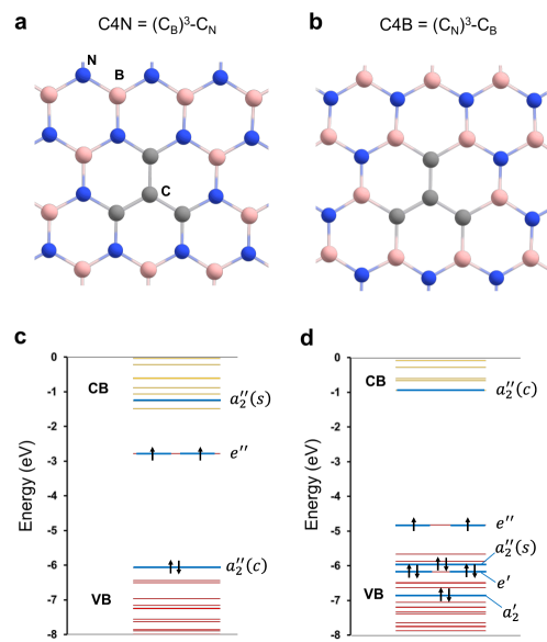
Here, we theoretically study the neutral charge state of the nitrogen and the boron centred symmetric carbon tetramer structures in hBN, i.e. (C)3-C and (C)3-C that we dub as C4N and C4B, respectively. The electronic structures of the defects consist of a triplet ground state, an optically allowed triplet excited state, and two singlet states between the triplets. For the C4B defect, we obtain large inter-system crossing rate from the triplet excited state to the singlet manifold and strain dependent inter-system crossing rate to the ground state. For the C4N defect, the spin selective decay is enabled by out-of-plane distortions. Therefore, strain can be used to engineer the defects’ inter-system crossing rates and contrast. In addition, the carbon tetramers gives rise to narrow magnetic resonance lines, due to the localization of the spin density on the spinless carbon atoms. Relying on our results, we propose the C4N and C4B defects in hBN as chemically stable spin qubits for improving sensing in low dimensions.
The thermodynamic properties of carbon complexes have been studied recently in the literature.[39, 47] Importantly, the symmetric C4N and C4B tetramers, see Fig. 1a and b, possess a surprisingly low formation energy. This can be explained by the Baird-aromatic stabilization of C4 containing hBN (i.e. there are two unpaired electrons and altogether electrons in the delocalized system of any selected set of rings; denotes an arbitrary integer), which is similarly favorable to the Hückel aromaticity of pure hBN (i. e. there are electrons in the delocalized system, all of which are paired). We note here that based on Baird’s and Hückel’s rules [48], the general conclusion can be drawn that even number of carbon atoms can, while odd number of carbon atoms cannot maintain aromaticity, implying larger formation energies in the latter case.
The formation energy of the neutral C4N and C4B defects are 2.5 eV (8.3 eV) and 8.7 eV (2.9 eV) in N-rich (B-rich) growth conditions and further decreases in charged configurations.[39] The most relevant charge transition levels are eV, eV, and eV for the C4N defect and eV, eV, and eV for the C4B defect measured from the valence band maximum.[39] The neutral charge state of the C4N (C4B) defect is thus stable in the upper half (lower half) of the band gap, where the Fermi energy is located in N-rich (N-poor) growth conditions.[39]
Results
The single particle electronic structures of the neutral ground state of the C4N and C4B defects are depicted in Fig. 1c and d, respectively. In-plane sp2 bonding states of the atoms are fully occupied and most of them fall deep in the valence band. The four orbitals of the carbon atoms form defect states that appear inside the band gap. In the neutral charge state of the C4N defect, the most relevant single particle defects states are the fully occupied state, the half occupied states, and the empty , see Fig. 1c. As visualized in Supplementary Figure S2, the and orbitals are primarily located on the central carbon atom and on the three side carbon atoms, respectively. orbital is strongly localized on the central carbon, while orbital is slightly delocalized and has significant contributions from the orbitals of the surrounding three boron atoms. The most relevant defects states for the C4B defect are the fully occupied and states, the half occupied state, and the empty , see Fig. 1d and Fig. S2. The occupied defect states of the C4B defect can be found closer to the valence band compared to the case of the C4N defect. For the C4B defect, a fully occupied in-plane bonding state can be found close to the valance band maximum and it plays an important role in the optical excitation process. Since the double degenerate state is occupied by two electrons with parallel spin, both defects exhibit a triplet ground state.
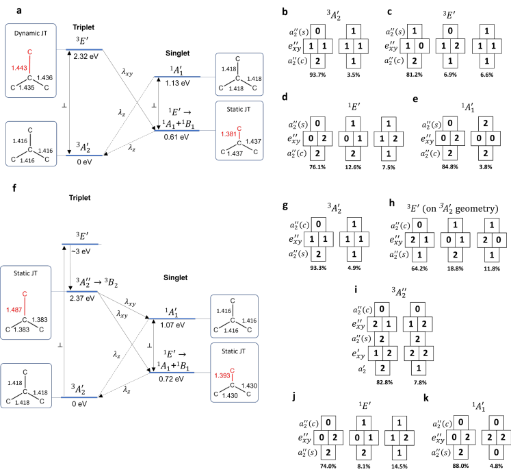
The many-body electronic structures of the symmetric carbon tetramers are schematically visualized in Fig. 2, where the energy gaps are obtained with an anticipated error margin of eV[49] on CASSCF-NEVPT2 level of theory[50]. As can be seen, four (five) states can be found in the low energy part of the electronic structure of the C4N (C4B) defect. The ground states of both defects can be described to a large degree (%) by the single Slater determinant obtained in the single particle picture in DFT, see Fig. 2c-d. For C4N, a triplet state can be found 2.32 eV above the ground state. (The corresponding zero phonon photoluminescence (ZPL) energy, which is obtained by adding the zero-point energy contribution of the local vibrational modes to the 2.32 eV adiabatic energy difference, was found to be 2.18 eV.) The optically excited state is largely described by the determinant corresponding to the transition, however, other determinants of single excitation mix with the leading term as depicted in Fig. 2c. Transition between the triplets is enabled by parallel to polarized photon absorption and emission. The state is Jahn-Teller (JT) unstable and the optimized structure is slight distorted, see Fig. 2a. Due to the small JT distortion, we expect a dynamic Jahn-Teller effect, where the vibronic state exhibits effective high symmetry. (Here, we note that an alternative, out-of-plane distorted triplet excited state geometry was also observed in some calculations, see Supplementary Information, Figure S5. This effect is however peculiar to single, separated hBN layers.) In between the triplet states, there are two singlet excited states, a state and a state 0.61 eV and 1.13 eV above the ground state energy level, respectively.
For the C4B defect, we obtain a similar many-body electronic structure as for the C4N defect; however, with an additional dark triplet excited state in-between the ground state and the triplet excited state, see Fig. 2a and f. The lower lying excited state and the optically excited state is expected to be found 2.37 eV and 3.0 eV above the ground state. (Note that the latter value is an estimation based on the vertical excitation energy of 3.7 eV at the geometry and approximate structural relaxation energy as the relaxation to geometry could not be performed due to the delocalization of the characteristic orbitals.) These states are described to a large degree by an transition and transition, respectively, see Fig. 2h and i. Both states are JT unstable and the point group symmetry of the optimized excited state structure reduces to C. The relaxed lowest energy triplet excited state belongs to the irreducible representation of C. In D symmetry, no optical transition is possible between the ground and the excited state. This property is largely preserved even in the JT distorted state. Transition to the higher lying state is possible, similarly to the C4N defect; however, due to the proximity of the state a rapid non-radiative decay to this lower lying triplet state is expected. Therefore, the C4B defect can be optically excited, but no PL emission is possible from this defect in the visible range. In addition to the triplets, we find two singlets, a state and a state 0.72 eV and 1.07 eV above the ground state, respectively.
Slater determinant expansion of the singlet states are also provided in Fig. 2b-e and Fig. 2g-k for the C4N and C4B defects. The most relevant and the states are the singlets that correspond to the ground state occupancy of the single particle orbitals. These singlets mix with other excited determinants to a similar degree as the optically excited states. The state is a Jahn-Teller unstable states and it goes through a severe structure distortion. In the optimized configuration one of the C-C bonds shortens that splits the state into a and a states in C2v symmetry, see Fig. 2a and f.
For the radiative lifetime of the triplet excited states of the C4N defect, we obtain 80.5 ns at 0 K using 2.13 refractive index for a 590 nm photon. From the computed dipole moment of the transition and harmonic vibrational analysis of the two individual electronic states, we calculate the phonon side band (PSB) of the C4N defect, see Fig. 3. We obtain 1.8 for the Huang Rhys factor (HR factor) that correspond to Debye Waller factors (DW factors) of 0.165. The relatively high DW factor for C4N defect is due to the high symmetry and small distortion of the excited state geometry. In addition, in symmetry we expect weak coupling to electric field for the C4N structure.[51]
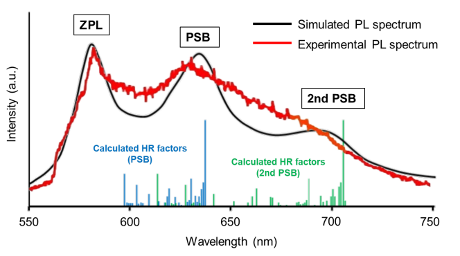
Partial HR factors of the vibrational modes indicate that the PL transitions couple strongest to in-plane carbon-carbon bond stretching modes that drive the JT distorted excited state into the symmetric ground state configuration (see section S3.3 of the Supplementary Information for the visualization of the vibrations). The energy of both modes is 0.196 eV (1583 cm-1), which corresponds to the generally observed range of aromatic C-C stretching in infrared spectroscopy.[52] On the other hand, additional lower energy modes also couple to the defect that broaden and shift the maximum of the resonance peaks of the calculated PL spectrum. The phonon side-band of the PL emission of the C4N defect is compared with the experimental PL spectrum[27, 28] of the unidentified carbon related quantum bit, see Figure 3. The theoretical and experimental spectra agree very well.
| C4N | C4B | ||||
| Transition | matrix element | Transition | matrix | ||
| 0 K static | Buckling | Buckling | element | ||
| (=0°) | (=2.7°) | (=6.9°) | 0 K static | ||
| 0 | 16.03 | 31.95 | 27.08 | ||
| 0.03 | 0.03 | 0.18 | 0 | ||
| 0 | 7.67 | 13.26 | 48.81 | ||
| 0.45 | 4.65 | 14.94 | 0 | ||
| 0 | 0.26 | 0.15 | 0 | ||
| 2.76 | 2.61 | 11.25 | 2.71 | ||
| 0 | 6.41 | 9.53 | 0 | ||
| 0.27 | 0.24 | 1.47 | 0.06 | ||
Point defect quantum bits are a special type of color centers that exhibit high spin ground state and spin state dependent optical emission through spin selective non-radiative decay processes from the optically excited state to the ground state. As carbon tetramers possess high spin ground state and singlet shelving states between the triplet excited and ground states, they may implement optically addressable spin quantum bits in hBN that we investigate in the following.
In order to obtain an efficient spin state dependent non-radiative decay channel through the singlets, the triplet and the singlet manifolds should be coupled by strong spin-orbit coupling (SOC) matrix elements. For the C4B defect we obtain 48.81 GHz (27.08 GHz) spin-orbit coupling matrix elements between the () and the () states, see Table 1. Spin-orbit interaction thus gives rise to a decay channel with approximately 0.07 MHz decay rate for the dark excited triplet of the C4B defect. The spin-orbit coupling matrix elements between the state and the ground state are weaker, enabled mostly by the Jahn-Teller distortion of the low lying singlet state. Consequently, the state is long-lived compared to the triplet excited state. These results indicate that the C4B defect can be spin polarized through an optical excitation to the state and subsequent non-radiative and spin selective decay through the , , and states. Due to this behaviour, the C4B defect may observed in electron spin resonance (ESR) measurement in low concentrations under 3.0 eV excitation. In addition, due to the strict spin selectivity of the non-radiative decay from the excited state and the expectedly long lifetime of the () state, the defect may be suitable for photoelectron detected magnetic resonance (PDMR) read-out of the spin states.
The C4N defect’s lowest energy triplet excited state has a different symmetry than the excited state of the C4B defect, therefore, the spin-orbit coupling between the triplets and the singlets is forbidden in first order approximation in D3h symmetry. Indeed, considering the 0 K static atomic structure and corresponding many-particle electronic states, we obtain either zero or small spin-orbit coupling matrix elements between the states on CASSCF-NEVPT2 level of theory, see Table 1, left column. The non-zero elements are due to the JT effect that give rise to weak couplings between states. On the other hand, strain and out-of-plane distortions may break the symmetry that could give rise to a sizable increases of the spin-orbit coupling matrix elements for C4N. For example, in-plane compression of hBN flakes causes the sample to buckle, which can be quantified by the dihedral angle given by the position of the 4 carbon atoms (denoted as in Table 1). equals to 0° in the equilibrium geometry as all C atoms are located in one plane, but it shows an increasing deviation from 0° when enforcing the side of the flake - i.e. the outside B and N atoms - to remain in fixed position closer and closer to the center (see section S3.2 of Supplementary Information for representative geometries). Buckling of hBN, which is commonly observed in experiments [28], can give rise to spin-orbit matrix elements in the 10-30 GHz range that are comparable with NV center’s matrix elements.[53] The increased SOC matrix elements give rise to spin dependent non-radiative dacay channels that may facilitate optical read-out of the spin state.
As a demonstrative example, we computed the photoluminescence and inter-system crossing rates between the electronic states of the buckled flake at =6.9° - see section S3.4 of the Supplementary Information. The obtained data indicate polarizability in state. These results demonstrate that the C4N defect can implement an optically addressable spin qubit, whose spin dependent optical signal is enabled mostly by local strain.
Apart from strain induced geometry distortions, the out-of-plane vibration of the C4 center may also give rise to significant SOC matrix elements and - consequently - intersystem crossing rates in the case of C4N. Namely, even though the matrix elements are zero (or close to zero) in equilibrium geometry, it does not hold true for non-equilibrium geometries where the system spends a significant amount of time due to its constant vibration (See Table S6 for SOC matrix elements computed at geometries displaced along the out-of-plane normal mode). Thus, a Herzberg-Teller transition[54] is possible, the rate of which strongly depends on the occupancy of vibrational levels (i. e. the temperature).
| C4N | C4B | ||||||||||
|---|---|---|---|---|---|---|---|---|---|---|---|
| site | N | site | N | ||||||||
| Cc | 1 | -33.4 | -33.4 | -57.6 | 0.0 | Cc | 1 | -22.9 | -22.9 | -48.0 | 0.0 |
| Cs | 3 | 8.6 | 8.8 | 95.0 | 0.0 | Cs | 3 | -2.6 | -2.6 | 68.9 | 0.0 |
| N1 | 6 | -3.2 | -3.3 | 0.3 | 0.1 | B1 | 6 | -10.6 | -8.5 | -6.8 | -0.2 |
| B2 | 3 | -0.6 | -0.3 | 1.7 | 0.0 | N2 | 3 | -0.5 | -0.3 | 1.5 | 0.0 |
| B3 | 6 | 0.2 | -0.9 | 1.5 | 0.3 | N3 | 6 | -0.1 | -0.4 | 1.1 | 0.0 |
| BA/B | 2 | -0.3 | -0.3 | 0.6 | 0.0 | BA/B | 6 | -0.2 | -0.2 | 0.6 | 0.0 |
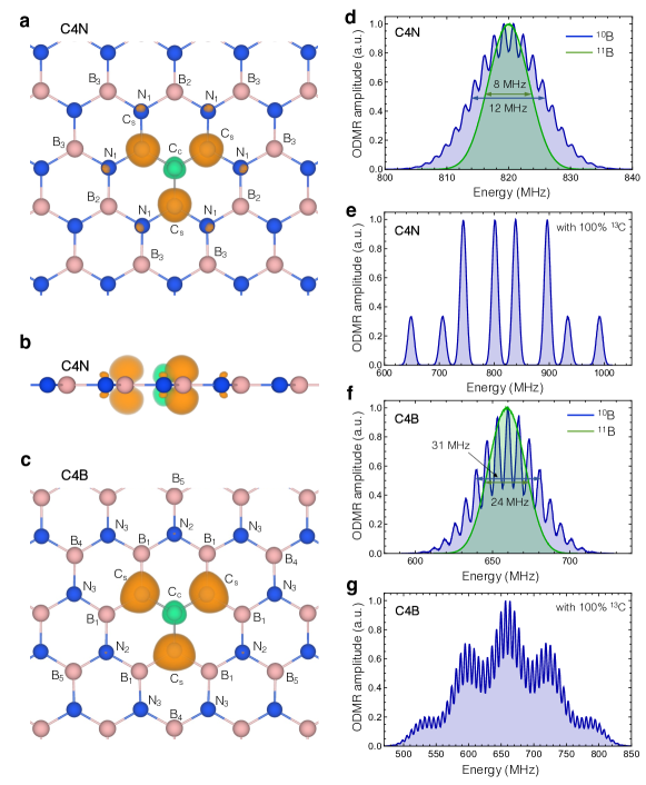
Finally, we present our result on the spin properties of the C4N and C4B defects. For the zero-field splitting (ZFS) parameter of the C4N defect we obtain 820 MHz and 840 MHz with CASSCF-NEVPT2 and periodic hybrid-DFT with spin contamination error correction[55], respectively. The difference of the values indicate the error margin of our ZFS calculations. For the C4B defect we obtain a slightly reduced MHz ZFS value on CASSCF-NEVPT2 level of theory. Due to the D3h symmetry, the quantization axis of the defects is parallel to the -axis and no splitting is observed in unstrained configurations. The spin density of the defects and the locations of the most relevant nuclear spins are depicted in Fig. 4a-c. The corresponding hyperfine coupling parameters, obtained with periodic hybrid-DFT in a bulk model, are provided in Table 2 and in section S3.6 of the Supplementary Information. Most notably, the spin density localizes mainly on the carbon atoms and only secondary localization can be found on the first neighbor nitrogen atoms. Accordingly, the carbon hyperfine parameters an order of magnitude larger than the rest of the coupling parameters. Using the theoretical spin coupling parameters, the predicted electron spin resonance (ESR) spectra at zero magnetic field for different isotope abundances are depicted in Fig. 4d-g. In natural abundance, 13C nuclear spin can be found only with 1.07% probability, thus in most configurations no carbon spins are included in the structures. When completely ignoring carbon nuclear spins, we obtain a narrow homogeneous ESR signal, where the line width is determined by the boron hyperfine coupling tensor and the boron isotope abundance. The full widths of the resonance peaks at half maximum are 12 MHz (8 MHz) and 31 MHz (24 MHz) for the C4N and the C4B defects in 10BN (11BN) sample. The narrow ESR line width may make the C4N and C4B defects attractive candidates for sensing. When carbon nuclear spins are included with 100% abundance, we observe a characteristic 8 peak hyperfine structure with 95.0 and 57.6 MHz splittings for the C4N defect, see Fig. 4e, and a characteristic 5 broad peak structure with 60 MHz splitting. 13C enriched carbon contamination and observation of the carbon related hypefine structure can be used to unambiguously identify the C4N and C4B defects.
Discussions
Sensing applications
Recently, few nanometers thick sensing foils has been developed by using spin qubit-containing hBN sheets.[16, 17, 18] In order to maximally utilize the layered structure of hBN and to further boost sensitivity and spatial resolution in such experiments, single sheet hBN flakes with stable point defect spin qubits are needed. We propose here the charge neutral symmetric carbon tetramers for implementing such chemically stable quantum bits in hBN. Due to the bond-formations, the carbon tetramers can give rise to atomic thin sensing foils that may be stable even at ambient conditions. Furthermore, the narrow electron spin resonance linewidth of the nitrogen centered carbon tetramer may lead to high sensitivity.
Robust spin qubits could also be highly beneficial for hBN-based dynamic nuclear polarization.[42] We show here that carbon tetramers can be spin polarized by optical illumination, leading to a spin polarization sources that may couple to nuclear spins outside the hBN host. Since the symmetric carbon tetramers can be stable at the surface in close proximity to other molecules, e.g. the NMR agent tetramethylsilane, efficient polarization transfer could be achieved between the quantum defects and the molecules on the surface. High-temperature and low-magnetic nuclear hyperpolarization mechanism are long-time sought for for boosting the sensitivity of conventional NMR and MRI applications.
Stable spin qubits are key components of both of the above-mentioned applications. Since, the symmetric carbon tetramers improve on the state of the art in this respect, they could lead to advances in nanoscale sensing.
Fabrication
Previous computational studies[39] have demonstrated that carbon tetramers exhibit low formation energy in N-rich samples that may imply the formation of these complex defects in observable concentrations ( cm-3) in hBN. After growth treatments, however, may give rise to concentrations well exceeding the thermal equilibrium values and enable on-demand fabrication in few layer samples. In this respect, carbon implantation maybe of high importance that can create carbon related point defect quantum bits in hBN.[27] Furthermore, scanning transmission electron microscope (STEM) is also of high potential for sub-nanometer precision creation of defects.[56] STEM mapping combined with a subsequent annealing steps allows the creation of the carbon complexes in single layer hBN samples.[56] These processes open up new directions for tailored fabrication of carbon clusters, including the symmetric C4N defect, in hBN.
Summary
In this paper we comprehensively studied the neutral nitrogen and boron site centered symmetric carbon tetramers in hBN. By using complementary first principles methods, we predicted the electronic structure as well as the optical and spin properties of the defects. We showed that symmetric carbon tetrameters exhibit high spin ground state, optical transition in the visible range, singlet shelving states, and strain dependent non-radiative decay channels. We concluded that the C4N and C4B defects can implement chemically stable spin qubit that may remain functional on the surface even at ambient conditions, in contrast to the established vacancy related quantum defects. Furthermore, strain can be used to tailor the spin contrast of the defects, which is a new feature for spin quantum bits in hBN.
Methods
In this study, we carried out first principles calculations of both periodic, supercell model and molecule model of the symmetric C4 defects in hBN. The two approaches allowed independent computational studies on different levels of theory, ensuring the reliability of our results. Below we briefly summarize the computational protocols; the detailed description of the methodology (including sample input files for the sake of reproducibility) can be found in the Supplementary Information.
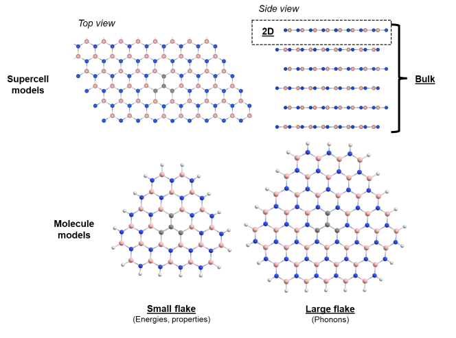
Computations with supercell models
Kohn-Sham density functional theory was employed to study the periodic models of carbon tetramer defects with VASP package[57]. Here, we considered a plane wave basis set of 450 eV, PAW[58] core potentials, and HSE06 hybrid exchange-correlation functional[59] with 0.32 exact exchange fraction[46]. The defects were modeled in 162-atom (monolayer) and 768-atom (bulk) supercells (Fig. 5, top). To account for van der Waals interaction, we included the D3 correction by Grimme et al[60]. The ZPL energies were calculated from the energy difference between ground and excited states, where the excited states were obtained using spin-conserved constrained DFT method[61] without enforcing symmetry restrictions.
Computations with molecule models
As a reasonable compromise between cost and accuracy, two hBN flakes of different size were used to investigate the C4 defects as a finite molecule. Electronic energies and properties (e.g. transition dipole moments) were computed on a smaller model (Fig. 5, bottom left), while phononic effects were calculated on a larger system (Fig. 5, bottom right). Test calculations justifying the choice of flake size can be found in the Supplementary Information. All calculations were carried out using the ORCA 5.0.3. program[62].
Geometry optimizations and vibrational analyses were performed using density functional theory, at PBE0/cc-pVDZ level[63, 64] with D3(BJ) dispersion correction[65]. In the case of excited states, time-dependent density functional theory (TD-DFT)[66] was requested with 10 roots. Singlet excited states were generated from the triplet ground state by spin-flip[67].
Single-point energies and electronic properties were determined at CASSCF/cc-pVTZ level of theory[68, 64] while dynamic correlation energy was taken into account by second-order N-electron valence perturbation theory (NEVPT2)[50]. The active orbital space for CASSCF was constructed based on both time-dependent density functional theory results obtained by ORCA and density matrix renormalization group (DMRG)[69, 70] calculations using the Budapest-DMRG package[71].
Acknowledgments
This research was supported by the National Research, Development, and Innovation Office of Hungary within the Quantum Information National Laboratory of Hungary (Grant No. 2022-2.1.1-NL-2022-00004) and within grants FK 135496 and FK 145395. V.I. also appreciates support from the Knut and Alice Wallenberg Foundation through WBSQD2 project (Grant No. 2018.0071). O.L. was supported by the Center for Scalable and Predictive methods for Excitation and Correlated phenomena (SPEC), funded as part of the Computational Chemical Sciences Program by the U.S. Department of Energy (DOE), Office of Science, Office of Basic Energy Sciences, Division of Chemical Sciences, Geosciences, and Biosciences at Pacific Northwest National Laboratory. The calculations were performed on resources provided by the Swedish National Infrastructure for Computing (SNIC) at the National Supercomputer Centre (NSC). We acknowledge KIFÜ for awarding us access to computational resource based in Hungary. Z.B. and T.S. would like to thank the University of Alabama and the Office of Information Technology for providing high performance computing resources and support that have contributed to these research results.
Data availability
The data that support the findings of this study are available from the authors upon reasonable request.
Author contributions
Z.B., R.B, and A.G. carried out the first principles calculations, O.L. developed the DMRG program package. V.I., Z.B., and G.B. wrote the manuscript with inputs from all coauthors. The work was supervised by V.I. and G.B.
Competing interests
The authors declare no competing interests.
References
References
- [1] Wang, Q. H., Kalantar-Zadeh, K., Kis, A., Coleman, J. N. & Strano, M. S. Electronics and optoelectronics of two-dimensional transition metal dichalcogenides. Nature Nanotechnology 7, 699–712 (2012). URL https://www.nature.com/articles/nnano.2012.193.
- [2] Manzeli, S., Ovchinnikov, D., Pasquier, D., Yazyev, O. V. & Kis, A. 2d transition metal dichalcogenides. Nature Reviews Materials 2, 1–15 (2017). URL https://www.nature.com/articles/natrevmats201733.
- [3] Geim, A. K. & Grigorieva, I. V. Van der Waals heterostructures. Nature 499, 419–425 (2013). URL https://www.nature.com/articles/nature12385.
- [4] Liang, S.-J., Cheng, B., Cui, X. & Miao, F. Van der Waals heterostructures for high-performance device applications: Challenges and opportunities. Advanced Materials 32, 1903800 (2020). URL https://onlinelibrary.wiley.com/doi/abs/10.1002/adma.201903800.
- [5] Jelezko, F., Gaebel, T., Popa, I., Gruber, A. & Wrachtrup, J. Observation of coherent oscillations in a single electron spin. Physical Review Letters 92, 076401 (2004). URL http://link.aps.org/abstract/PRL/v92/e076401.
- [6] Doherty, M. W. et al. The nitrogen-vacancy colour centre in diamond. Physics Reports 528, 1 – 45 (2013). URL http://www.sciencedirect.com/science/article/pii/S0370157313000562.
- [7] Widmann, M. et al. Coherent control of single spins in silicon carbide at room temperature. Nat. Mater. 14, 164–168 (2015). URL http://dx.doi.org/10.1038/nmat4145.
- [8] Taylor, J. M. et al. High-sensitivity diamond magnetometer with nanoscale resolution. Nature Physics 4, 810–816 (2008). URL https://www.nature.com/articles/nphys1075.
- [9] Schirhagl, R., Chang, K., Loretz, M. & Degen, C. L. Nitrogen-vacancy centers in diamond: Nanoscale sensors for physics and biology. Annual Review of Physical Chemistry 65, 83–105 (2014). URL https://doi.org/10.1146/annurev-physchem-040513-103659.
- [10] Barry, J. F. et al. Sensitivity optimization for NV-diamond magnetometry. Reviews of Modern Physics 92, 015004 (2020). URL https://link.aps.org/doi/10.1103/RevModPhys.92.015004.
- [11] Stürner, F. M. et al. Integrated and portable magnetometer based on nitrogen-vacancy ensembles in diamond. arXiv:2012.01053 [cond-mat] (2020). URL http://arxiv.org/abs/2012.01053. cond-mat/2012.01053.
- [12] Zhang, T. et al. Toward quantitative bio-sensing with nitrogen–vacancy center in diamond. ACS Sensors 6, 2077–2107 (2021). URL https://doi.org/10.1021/acssensors.1c00415.
- [13] Kaviani, M. et al. Proper surface termination for luminescent near-surface NV centers in diamond. Nano Letters 14, 4772–4777 (2014). URL https://doi.org/10.1021/nl501927y.
- [14] Kim, M. et al. Decoherence of near-surface nitrogen-vacancy centers due to electric field noise. Phys. Rev. Lett. 115, 087602 (2015). URL https://link.aps.org/doi/10.1103/PhysRevLett.115.087602.
- [15] Dwyer, B. L. et al. Probing spin dynamics on diamond surfaces using a single quantum sensor. PRX Quantum 3, 040328 (2022). URL https://link.aps.org/doi/10.1103/PRXQuantum.3.040328.
- [16] Tetienne, J.-P. Quantum sensors go flat. Nature Physics 1–2 (2022). URL https://www.nature.com/articles/s41567-021-01338-5.
- [17] Healey, A. J. et al. Quantum microscopy with van der waals heterostructures. Nature Physics 1–5 (2022). URL https://www.nature.com/articles/s41567-022-01815-5.
- [18] Kumar, P. et al. Magnetic imaging with spin defects in hexagonal boron nitride. Physical Review Applied 18, L061002 (2022). URL https://link.aps.org/doi/10.1103/PhysRevApplied.18.L061002.
- [19] Gottscholl, A. et al. Spin defects in hBN as promising temperature, pressure and magnetic field quantum sensors. Nature Communications 12, 4480 (2021). URL https://www.nature.com/articles/s41467-021-24725-1.
- [20] Liu, W. et al. Temperature-dependent energy-level shifts of spin defects in hexagonal boron nitride. ACS Photonics 8, 1889–1895 (2021). URL https://doi.org/10.1021/acsphotonics.1c00320.
- [21] Lyu, X. et al. Strain quantum sensing with spin defects in hexagonal boron nitride. Nano Letters 22, 6553–6559 (2022). URL https://doi.org/10.1021/acs.nanolett.2c01722.
- [22] Caldwell, J. D. et al. Photonics with hexagonal boron nitride. Nature Reviews Materials 4, 552–567 (2019). URL https://www.nature.com/articles/s41578-019-0124-1.
- [23] Sajid, A., Ford, M. J. & Reimers, J. R. Single-photon emitters in hexagonal boron nitride: a review of progress. Reports on Progress in Physics 83, 044501 (2020). URL https://doi.org/10.1088/1361-6633/ab6310.
- [24] Tran, T. T., Bray, K., Ford, M. J., Toth, M. & Aharonovich, I. Quantum emission from hexagonal boron nitride monolayers. Nature Nanotechnology 11, 37–41 (2016). URL https://www.nature.com/articles/nnano.2015.242.
- [25] Gottscholl, A. et al. Initialization and read-out of intrinsic spin defects in a van der waals crystal at room temperature. Nature Materials 1–6 (2020). URL https://www.nature.com/articles/s41563-020-0619-6.
- [26] Chejanovsky, N. et al. Single-spin resonance in a van der Waals embedded paramagnetic defect. Nature Materials 20, 1079–1084 (2021). URL https://www.nature.com/articles/s41563-021-00979-4.
- [27] Mendelson, N. et al. Identifying carbon as the source of visible single-photon emission from hexagonal boron nitride. Nature Materials 20, 321–328 (2020). URL https://www.nature.com/articles/s41563-020-00850-y.
- [28] Stern, H. L. et al. Room-temperature optically detected magnetic resonance of single defects in hexagonal boron nitride. Nature Communications 13, 618 (2022). URL https://www.nature.com/articles/s41467-022-28169-z.
- [29] Sajid, A. & Thygesen, K. S. VNCB defect as source of single photon emission from hexagonal boron nitride. 2D Materials 7, 031007 (2020). URL https://dx.doi.org/10.1088/2053-1583/ab8f61.
- [30] Babar, R. et al. Quantum sensor in a single layer van der Waals material. arXiv:2111.09589 [cond-mat] (2021). URL http://arxiv.org/abs/2111.09589. 2111.09589.
- [31] Bhang, J., Ma, H., Yim, D., Galli, G. & Seo, H. First-principles predictions of out-of-plane group IV and V dimers as high-symmetry, high-spin defects in hexagonal boron nitride. ACS Applied Materials & Interfaces 13, 45768–45777 (2021). URL https://doi.org/10.1021/acsami.1c16988.
- [32] Liu, W. et al. Spin-active defects in hexagonal boron nitride. Materials for Quantum Technology 2, 032002 (2022). URL https://dx.doi.org/10.1088/2633-4356/ac7e9f.
- [33] Ivády, V. et al. Ab initio theory of the negatively charged boron vacancy qubit in hexagonal boron nitride. npj Computational Materials 6, 1–6 (2020). URL https://www.nature.com/articles/s41524-020-0305-x.
- [34] Haykal, A. et al. Decoherence of spin defects in monoisotopic hexagonal boron nitride. Nature Communications 13, 4347 (2022). URL https://www.nature.com/articles/s41467-022-31743-0.
- [35] Liu, W. et al. Coherent dynamics of multi-spin center in hexagonal boron nitride. Nature Communications 13, 5713 (2022). URL https://www.nature.com/articles/s41467-022-33399-2.
- [36] Jara, C. et al. First-principles identification of single photon emitters based on carbon clusters in hexagonal boron nitride. The Journal of Physical Chemistry A 125, 1325–1335 (2021). URL https://doi.org/10.1021/acs.jpca.0c07339.
- [37] Li, K., Smart, T. J. & Ping, Y. Carbon trimer as a 2 eV single-photon emitter candidate in hexagonal boron nitride: A first-principles study. Physical Review Materials 6, L042201 (2022). URL https://link.aps.org/doi/10.1103/PhysRevMaterials.6.L042201.
- [38] Golami, O. et al. Ab initio and group theoretical study of properties of a carbon trimer defect in hexagonal boron nitride. Physical Review B 105, 184101 (2022). URL https://link.aps.org/doi/10.1103/PhysRevB.105.184101.
- [39] Maciaszek, M., Razinkovas, L. & Alkauskas, A. Thermodynamics of carbon point defects in hexagonal boron nitride. Phys. Rev. Materials 6, 014005 (2022). URL https://link.aps.org/doi/10.1103/PhysRevMaterials.6.014005.
- [40] Gao, X. et al. High-contrast plasmonic-enhanced shallow spin defects in hexagonal boron nitride for quantum sensing. Nano Letters 21, 7708–7714 (2021). URL https://doi.org/10.1021/acs.nanolett.1c02495.
- [41] Murzakhanov, F. F. et al. Electron–nuclear coherent coupling and nuclear spin readout through optically polarized VB– spin states in hBN. Nano Letters 22, 2718–2724 (2022). URL https://doi.org/10.1021/acs.nanolett.1c04610.
- [42] Gao, X. et al. Nuclear spin polarization and control in hexagonal boron nitride. Nature Materials 1–5 (2022). URL https://www.nature.com/articles/s41563-022-01329-8.
- [43] Sajid, A., Thygesen, K. S., Reimers, J. R. & Ford, M. J. Edge effects on optically detected magnetic resonance of vacancy defects in hexagonal boron nitride. Communications Physics 3, 1–8 (2020). URL https://www.nature.com/articles/s42005-020-00416-z.
- [44] Reimers, J. R. et al. Photoluminescence, photophysics, and photochemistry of the defect in hexagonal boron nitride. Physical Review B 102, 144105 (2020). URL https://link.aps.org/doi/10.1103/PhysRevB.102.144105.
- [45] Barcza, G. et al. DMRG on top of plane-wave Kohn–Sham orbitals: A case study of defected boron nitride. Journal of Chemical Theory and Computation 17, 1143–1154 (2021). URL https://doi.org/10.1021/acs.jctc.0c00809.
- [46] Weston, L., Wickramaratne, D. & Van de Walle, C. G. Publisher’s note: Hole polarons and -type doping in boron nitride polymorphs [phys. rev. b 96, 100102(r) (2017)]. Phys. Rev. B 97, 019908 (2018). URL https://link.aps.org/doi/10.1103/PhysRevB.97.019908.
- [47] Huang, P. et al. Carbon and vacancy centers in hexagonal boron nitride. Phys. Rev. B 106, 014107 (2022). URL https://link.aps.org/doi/10.1103/PhysRevB.106.014107.
- [48] Sung, Y. M. et al. Reversal of Hückel (anti)aromaticity in the lowest triplet states of hexaphyrins and spectroscopic evidence for Baird’s rule. Nature Chemistry 7, 418–422 (2015). URL https://doi.org/10.1038/nchem.2233.
- [49] Sarkar, R., Loos, P.-F., Boggio-Pasqua, M. & Jacquemin, D. Assessing the performances of CASPT2 and NEVPT2 for vertical excitation energies. Journal of Chemical Theory and Computation 18, 2418–2436 (2022). URL https://doi.org/10.1021/acs.jctc.1c01197.
- [50] Angeli, C., Cimiraglia, R., Evangelisti, S., Leininger, T. & Malrieu, J.-P. Introduction of n-electron valence states for multireference perturbation theory. The Journal of Chemical Physics 114, 10252–10264 (2001). URL https://doi.org/10.1063/1.1361246.
- [51] Zhigulin, I. et al. Stark effect of quantum blue emitters in hBN. URL http://arxiv.org/abs/2208.00600. 2208.00600 [physics, physics:quant-ph].
- [52] Lin-Vien, D., Colthup, N. B., Fateley, W. G. & Grasselli, J. G. Chapter 17 - aromatic and heteroaromatic rings. In Lin-Vien, D., Colthup, N. B., Fateley, W. G. & Grasselli, J. G. (eds.) The Handbook of Infrared and Raman Characteristic Frequencies of Organic Molecules, 277–306 (Academic Press, San Diego, 1991). URL https://www.sciencedirect.com/science/article/pii/B9780080571164500237.
- [53] Thiering, G. & Gali, A. Ab initio calculation of spin-orbit coupling for an NV center in diamond exhibiting dynamic Jahn-Teller effect. Physical Review B 96, 081115 (2017). URL https://link.aps.org/doi/10.1103/PhysRevB.96.081115.
- [54] Manian, A., Shaw, R. A., Lyskov, I., Wong, W. & Russo, S. P. Modeling radiative and non-radiative pathways at both the Franck-Condon and Herzberg-Teller approximation level. J. Chem. Phys. 155, 054108 (2021).
- [55] Biktagirov, T., Schmidt, W. G. & Gerstmann, U. Spin decontamination for magnetic dipolar coupling calculations: Application to high-spin molecules and solid-state spin qubits. Physical Review Research 2, 022024 (2020). URL https://link.aps.org/doi/10.1103/PhysRevResearch.2.022024.
- [56] Park, H. et al. Atomically precise control of carbon insertion into hBN monolayer point vacancies using a focused electron beam guide. Small 17, 2100693 (2021). URL https://onlinelibrary.wiley.com/doi/abs/10.1002/smll.202100693.
- [57] Kresse, G. & Hafner, J. Ab initio molecular-dynamics simulation of the liquid-metal–amorphous-semiconductor transition in germanium. Phys. Rev. B 49, 14251–14269 (1994). URL http://link.aps.org/doi/10.1103/PhysRevB.49.14251.
- [58] Blöchl, P. E. Projector augmented-wave method. Phys. Rev. B 50, 17953–17979 (1994). URL http://link.aps.org/doi/10.1103/PhysRevB.50.17953.
- [59] Heyd, J., Scuseria, G. E. & Ernzerhof, M. Hybrid functionals based on a screened Ccoulomb potential. J. Chem. Phys. 118, 8207 (2003). URL http://dx.doi.org/10.1063/1.1564060.
- [60] Grimme, S., Antony, J., Ehrlich, S. & Krieg, H. A consistent and accurate ab initio parametrization of density functional dispersion correction (DFT-D) for the 94 elements h-pu. The Journal of Chemical Physics 132, 154104 (2010). URL https://doi.org/10.1063/1.3382344. https://doi.org/10.1063/1.3382344.
- [61] Gali, A., Janzén, E., Deák, P., Kresse, G. & Kaxiras, E. Theory of spin-conserving excitation of the center in diamond. Phys. Rev. Lett. 103, 186404 (2009). URL https://link.aps.org/doi/10.1103/PhysRevLett.103.186404.
- [62] Neese, F. Software update: The ORCA program system—version 5.0. Wiley Interdisciplinary Reviews: Computational Molecular Science 12, e1606 (2022).
- [63] Adamo, C. & Barone, V. Toward reliable density functional methods without adjustable parameters: The PBE0 model. The Journal of Chemical Physics 110, 6158–6170 (1999). URL https://doi.org/10.1063/1.478522. https://doi.org/10.1063/1.478522.
- [64] Dunning, T. H. Gaussian basis sets for use in correlated molecular calculations. I. The atoms boron through neon and hydrogen. The Journal of Chemical Physics 90, 1007–1023 (1989). URL https://doi.org/10.1063/1.456153. https://doi.org/10.1063/1.456153.
- [65] Grimme, S., Ehrlich, S. & Goerigk, L. Effect of the damping function in dispersion corrected density functional theory. Journal of Computational Chemistry 32, 1456–1465 (2011). URL https://onlinelibrary.wiley.com/doi/abs/10.1002/jcc.21759.
- [66] Neese, F. Prediction of molecular properties and molecular spectroscopy with density functional theory: From fundamental theory to exchange-coupling. Coordination Chemistry Reviews 253, 526–563 (2009). URL https://www.sciencedirect.com/science/article/pii/S0010854508001197.
- [67] Casanova, D. & Krylov, A. I. Spin-flip methods in quantum chemistry. Phys. Chem. Chem. Phys. 22, 4326–4342 (2020). URL http://dx.doi.org/10.1039/C9CP06507E.
- [68] Kollmar, C., Sivalingam, K., Helmich-Paris, B., Angeli, C. & Neese, F. A perturbation-based super-CI approach for the orbital optimization of a CASSCF wave function. Journal of Computational Chemistry 40, 1463–1470 (2019). URL https://onlinelibrary.wiley.com/doi/abs/10.1002/jcc.25801.
- [69] Freitag, L. & Reiher, M. The Density Matrix Renormalization Group for Strong Correlation in Ground and Excited States, chap. 7, 205–245 (John Wiley and Sons, Ltd, 2020). URL https://onlinelibrary.wiley.com/doi/abs/10.1002/9781119417774.ch7.
- [70] Szalay, S. et al. Tensor product methods and entanglement optimization for ab initio quantum chemistry. International Journal of Quantum Chemistry 115, 1342–1391 (2015). URL https://onlinelibrary.wiley.com/doi/abs/10.1002/qua.24898.
- [71] Legeza, Ö., Veis, L. & Mosoni, T. QC-DMRG-Budapest, a program for quantum chemical DMRG calculations.