Control of light emission of quantum emitters coupled to silicon nanoantenna using cylindrical vector beams
Abstract
Light emission of europium (Eu3+) ions placed in the vicinity of optically resonant nanoantennas is usually controlled by tailoring the local density of photon states (LDOS). We show that the polarization and shape of the excitation beam can also be used to manipulate light emission, as azimuthally or radially polarized cylindrical vector beam offers to spatially shape the electric and magnetic fields, in addition to the effect of silicon nanorings (Si-NRs) used as nanoantennas. The photoluminescence mappings of the Eu3+ transitions and the Si phonon mappings are strongly dependent of both the excitation beam and the Si-NR dimensions. The experimental results of Raman scattering and photoluminescence are confirmed by numerical simulations of the near-field intensity in the Si nanoantenna and in the Eu3+-doped film, respectively. The branching ratios obtained from the experimental PL maps also reveal a redistribution of the electric and magnetic emission channels. Our results show that it is possible to spatially control both electric and magnetic dipolar emission of Eu3+ ions by switching the laser beam polarization, hence the near-field at the excitation wavelength, and the electric and magnetic LDOS at the emission wavelength. This paves the way for optimized geometries taking advantage of both excitation and emission processes.
Introduction
Enhancing and controlling the light emission of quantum emitters coupled to optically resonant nanostructures is essential for new light sources at the nanoscale, and for enhanced spectroscopies and biosensing krasnok_spectroscopy_2018 . The photoluminescence (PL) intensity of a quantum emitter at a position coupled to a nanoantenna is influenced by three parameters, as expressed in the following equation koenderink_single-photon_2017 ; bidault_dielectric_2019 :
| (1) |
where is the excitation rate, proportional to the excitation pump, is the quantum yield related to the local density of photon states (LDOS) at the emission angular frequency , and is the collection efficiency, that depends on both the emission directivity and detection geometry.
Many works have been devoted to LDOS engineering li_enhancing_2017 ; sanz-paz_enhancing_2018 ; mignuzzi_nanoscale_2019 ; brule_magnetic_2022 or to emission directivity curto_unidirectional_2010 ; poumirol_unveiling_2020 ; wiecha_design_2019 ; humbert_large-scale_2023 , but the influence of the pump has been rarely considered experimentally. In fact, the PL signal of a quantum emitter is either proportional to the LDOS or to the near-field intensity when the excited state is saturated or not, respectively girard_generalized_2005 ; wiecha_enhancement_2019 ; majorel_quantum_2020 . In this article, we investigate in the nonsaturated regime the influence of focused cylindrical vector beams on the PL of a rare earth ion-doped thin film deposited on high refractive index dielectric nanostructures.
Rare-earth ion-based quantum emitters have been widely studied over the last decade because they are photostable and present narrow electronic transitions, corresponding to efficient electric (ED) or magnetic (MD) dipole transitions, either at the absorption kasperczyk_excitation_2015 or at the emission karaveli_spectral_2011 ; aigouy_mapping_2014 . They have thus been used to probe the electric and magnetic components of light by placing them in the vicinity of plasmonic or dielectric antennas, where the electric and magnetic LDOS (E-LDOS and M-LDOS) can be adjusted and spatially separated aigouy_mapping_2014 ; mivelle_strong_2015 ; rabouw_europium-doped_2016 ; wiecha_enhancement_2019 . To some extent, enhancing electric or magnetic Purcell effect could lead to applications in telecommunication using near-infrared emitters such as Er3+ kalinic_all-dielectric_2020 , or efficient visible light sources and lamp phosphors using Eu3+ or Tb3+ baranov_modifying_2017 . The MD transitions, interacting with the magnetic components of light kasperczyk_excitation_2015 ; baranov_modifying_2017 ; wiecha_decay_2018 , may be even more interesting when they are coupled to high index dielectric nanoantennas, as in such nanostructures the magnetic field is known to be strongly enhanced at the magnetic dipole or quadrupole resonance wavelength rolly_promoting_2012 ; albella_low-loss_2013 ; bakker_magnetic_2015 ; matsumori_silicon_2022 . Experimentally, a larger enhancement of the MD emitting transition compared to the ED emitting transition has been reported wiecha_enhancement_2019 ; sugimoto_magnetic_2021 . Theoretically, a few recent works predict a very strong enhancement of the magnetic Purcell effect, larger than 103, in case of nanostructure design and M-LDOS optimization rocco_giant_2020 ; brule_magnetic_2022 .
Nevertheless, in addition to the nanoantenna design for tailoring the LDOS and the directional behavior as expressed in equation 1, the excitation beam is the third parameter that can be used to spatially and spectrally shape the intensity of any optically driven light source. Cylindrical vector beams (CVB) of radial or azimuthal polarization can very helpful as the electric and magnetic fields are spatially separated dorn_sharper_2003 ; kasperczyk_excitation_2015 , and can be used to selectively excite electric and magnetic resonance modes in dielectric nanoantennas wozniak_selective_2015 ; montagnac_engineered_2022 , as well as electric and magnetic dipole transitions in rare-earth ions kasperczyk_excitation_2015 .
We thus show in the following that CVB can be used to spatially engineer the PL intensity of Eu3+-doped thin films deposited on Si nanorings, due to different controlled near-field hot spots.
Experimental set-up and numerical tools
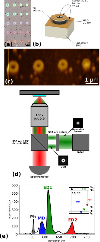
Si nanostructures are fabricated by electron beam lithography followed by reactive ion etching in a single crystal Si layer transferred on a fused silica (SiO2) substrate, referred to as silicon on silica (SOS). We chose nanorings (NRs) for their doughnut-like shape similar to the CVB symmetry. They are characterized by their outer radius and width , their height being fixed by the Si top layer of the SOS ( = 90 nm).
In figure 1a, we show a bright field image of the Si nanoresonators covered by a 20 nm-thick film obtained by low energy cluster beam deposition (LECBD) of Eu3+:Gd2O3 clusters wiecha_enhancement_2019 . The film homogeneity is very good as shown by atomic force microscope (AFM) image (see figure 1c). The distance between the Si-NR top surface and the Eu3+:Gd2O3 deposit is about 20 nm, corresponding to the thickness of the hydrogen silsesquioxane (HSQ) resist, which was left on top of the Si-NRs during the fabrication process to protect the smallest structures from etching or lift-off (see figure 1b). The HSQ resist optical constants are the same as the silica ones.
The photoluminescence (PL) mappings are obtained by raster scanning the sample under a laser beam tightly focused through a microscope objective of numerical aperture .
The excitation wavelength of 532 nm is resonant with the 7F1 5D1 electric dipole (ED) transition in Eu3+, and with a resonance mode of the Si-NRs (see supplemental information, Fig. S1) kasperczyk_excitation_2015 .
The linear polarization of the Gaussian excitation beam, referred to as lin-CVB, can be modified by a half-wave plate. The doughnut beam shape associated to azimuthal or radial polarization (referred to as azi-CVB and rad-CVB, respectively) is obtained by adding a Q-plate after the half-wave plate and before the microscope (figure 1d). We verified that the chosen polarization is conserved after reflection on the dichroic mirror.
In all cases, the power density on the sample was kept low enough to stay below the saturation regime of the excited state (see supplementary information), thus avoiding the PL being governed by the LDOS only. In the low power regime, as previously mentioned, we expect the PL to be dependent mainly on the near-field at the excitation wavelength girard_generalized_2005 ; wiecha_enhancement_2019 ; majorel_quantum_2020 .
A typical PL spectrum is displayed in figure 1. We will focus on three main features corresponding to 5D0 7F1 centered around 590 nm (MD transition), 5D0 7F2 around 610 nm (ED1 transition), and 5D0 7F4 around 690 nm (ED2 transition) aigouy_mapping_2014 ; kasperczyk_excitation_2015 . Notice that, when scanning the Si-NRs, the Raman spectrum due to two optical phonon processes can be detected (grey band in the spectrum), which is helpful defining precisely the position of the Si nanoantennas.
For electro-dynamical simulations, we used either the pyGDM toolkit implementing the Green Dyadic Method wiecha_pygdmpython_2018 , or the Meep software package based on the finite-difference time-domain (FDTD) method oskooi_meep_2010 .
Experimental results
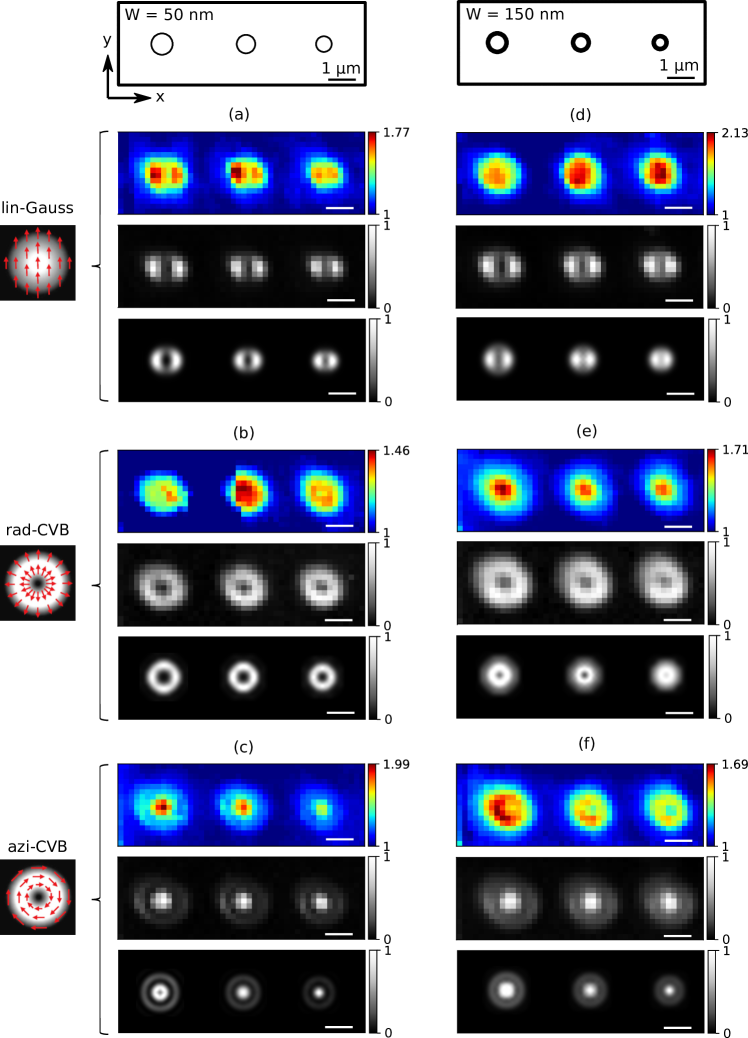
In the following, we address the Si Raman signal and the total PL intensity given by the integrated intensity of the three contributions. Typical PL and Raman scattering (RS) mappings are presented in figure 2. The main results that can be underlined are: (i) the RS maps are dependent on the excitation polarization only, and (ii) the PL maps not only depend of the excitation polarization but also on the Si-NR width .
Raman mappings of Si nanorings.
As shown in figure 2, the Raman mappings give the same signature for all nanorings for a given laser polarization. There are two lobes for the (vertical) linear polarization, a doughnut shape for the radial polarization, and a centered spot for the azimuthal polarization. The fact that the signal intensity map depends only on the laser polarization for a nanoring shape leads us to the assumption that the Raman signal is driven by the local electric field inside the nanoring dmitriev_resonant_2016 ; raza_raman_2021 . To prove this, we calculated by FDTD the electric-field intensity inside the Si-NR in each point of the raster scan of the laser beam. The simulations are also displayed in figure 2 below the experimental RS maps.
Both the experimental Raman maps and the calculated internal field intensity maps are in perfect agreement, validating our hypothesis.
Photoluminescence mappings of Eu3+:Gd2O3 deposited films on nanorings.
Confirming AFM images and previous experiments wiecha_enhancement_2019 , the cluster-deposited film is highly homogeneous as shown by the constant intensity observed in PL mappings far from the Si nanostructures.
There is a slight enhancement of the Eu3+ emission intensity above the Si-NR, but more important we point out a strong modification of the spatial distribution of the PL intensity as function of the excitation polarization. This spatial distribution is also strongly dependent on the nanoring dimensions in the case of the rad-CVB and azi-CVB excitations (See figure 2).
For linear polarized Gaussian beam, the PL enhancement evolves from two lobes for = 50 nm to a large central maximum with increasing width . For radial polarization, the PL enhancement evolves from a doughnut shape for = 50 nm to a narrow dotted maximum in a the ring center with increasing width . This behavior is fully reversed in the case of azimuthal polarization, with an evolution from narrow dotted maximum for = 50 nm to the doughnut shape with increasing width .
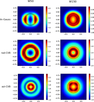
To understand these experimental results, we calculated using FDTD the electric near-field intensity distribution by raster scanning the different CVBs inside the Eu3+-doped film ( following a profile at 10 nm above the substrate surface and the Si-NR top surface including the HSQ layer). The near-field intensity distribution is calculated for each laser spot center position of the raster scan.
The results are given in figure 3 in the case of 400 nm radius Si-NRs with two selected widths = 50 nm and = 150 nm. There is a qualitative agreement between the near-field simulations of figure and the PL experiments. Indeed, in the case of the azi-CVB (bottom line of figures 2 and 3) , there is an obvious tendency for the near-field intensity maximum to form a doughnut above the Si-NR contour for the Si-NR with the largest width = 150 nm, to a reduced spot more centered inside the Si-NR contour for the narrowest = 50 nm. The behavior is reversed in the rad-CVB case (middle line of figures 2 and 3): large doughnut shape for = 50 nm and centered spot for = 150 nm. In the lin-CVB case, we observe an evolution from the two lobes for the narrowest to a larger central spot for the largest as in the PL maps.
As we chose the laser power to stay below the saturation regime (where the emission is driven by the LDOS) girard_generalized_2005 ; majorel_quantum_2020 , and that the excitation wavelength at 532 nm corresponds to an electric dipole transition kasperczyk_excitation_2015 , the good agreement with the electric near-field simulations shows that the PL is governed by the electric near-field distribution around and above the Si nanostructures. Our results also prove that the PL response can be tuned by the combination of Si nanoantennas and excitation beam shape and polarization.
Depending on these parameters, it is thus possible to have a narrow spotted PL maximum, which can be seen in both cases of azi-CVB and = 50 nm diameter Si-NR (Fig. 2c), and rad-CVB and = 150 nm diameter Si-NR (Fig. 2e). By increasing the objective NA or the local electric field intensity (for instance by decreasing both the nanoring and central hole diameters), we could expect an enhanced PL in a reduced spot size, improving considerably the spatial resolution. We point out that this effect could be even higher using the magnetic field with the appropriate excitation wavelength (527.5 nm) resonant with the 7F0 5D1 magnetic dipole transition in Eu3+ kasperczyk_excitation_2015 , as the magnetic field intensity is usually much larger than the electric field inside dielectric nanostructures bakker_magnetic_2015 ; yang_boosting_2017 . There is however an experimental challenge of filling a hole of about 50 nm in diameter by the emitters.
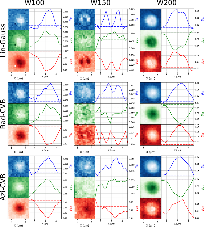
Branching ratios and influence of radiative LDOS and light collection. After having investigated how the total PL intensity could be controlled by the excitation beam, we now focus on the influence of the system on the different competing emission channels, referred to as MD, ED1 and ED2 centered around 590 nm, 610 nm and 700 nm, respectively (See the experimental set-up section and figure 1). The usual parameters used to describe how the emission channels are redistributed are the branching ratios, given by:
| (2) |
where is the integrated intensity of the transition labeled (MD, ED1, or ED2), is the sum of the the three contributions, is the radiative rate of the transition labeled , and is the sum of the radiative rates of each transition.
This method allows to connect the intensity measured in stationary PL experiments to the radiative electric and magnetic LDOS sanz-paz_enhancing_2018 ; rabouw_europium-doped_2016 ; chacon_vectorial_2022 .
We show in figure 4 the BR maps and 1D profiles for a Si-NR of 400 nm radius.
Though the influence of the excitation beam polarization is still visible, we point out the additional influence of the radiative LDOS as the BRs are affected as function of the Si-NR width. For the smallest (100 nm and below, left column of figure 4), the MD and ED1 emitting transitions tend to be favored to the detriment of ED2 transition. For the largest = 200 nm width, the MD is still enhanced while ED1 is now decreased to the benefit of ED2 (right column of figure 4). It seems that the =150 nm case corresponds to the transition between the extreme behaviors described above. Notice that the same behavior is found similar for different Si-NR radii (500-350 nm range) for a given value. The global behavior is also reproducible on different samples. The calculated magnetic and electric LDOS (not shown) do not fit the experiments, as the BRs depend only on the part of the radiative decay that enters the microscope objective rabouw_europium-doped_2016 . According to equation 1, more complex simulations are needed taking into account the LDOS , and the emission directivity and detection geometry .
We thus show that it is possible to shape the PL spatially, favoring different hot spots as function of the excitation beam polarization, while either enhancing or quenching a specific emission line of the Eu3+-doped film.
Conclusions
In conclusion, we investigated the photoluminescence mappings of Eu3+-doped cluster deposited films on Si nanorings using different cylindrical vector beams. In addition to the photon LDOS, we show that the excitation beam shape and polarization have an important effect. Radial and azimuthal polarized beams exciting ring shape nanoantennas allow to tune the near-field hot spots, hence the local PL enhancement. Our results show that it is possible to spatially shape the photoluminescence of quantum emitters coupled to dielectric nanoantennas by both the excitation and emission channels. More complex dielectric nanoantennas could be designed to be resonant at an absorption transition excited by a chosen cylindrical vector beam, and at a specific emitting transition while quenching others. Rare earth ions supporting magnetic transitions at both absorption and emission are very good candidates to benefit from a very high local magnetic field enhancement inside resonant dielectric nanoantennas at the excitation wavelength, combined to magnetic and electric LDOS engineering to control the different emission channels.
Acknowledgements
We acknowledge funding from Agence Nationale de la Recherche under project HiLight (ANR-19-CE24-0020-01), and support by the Toulouse computing facility HPC CALMIP (grants p12167 and p19042), and by the LAAS-CNRS micro and nanotechnologies platform, a member of the French RENATECH network. ICB is partner of the French Investissements d’Avenir program EUR-EIPHI (17-EURE-0002).
Author contributions
Each coauthor contributed.
Competing interests
The authors declare no competing interests.
References
- (1) Krasnok, A., Caldarola, M., Bonod, N. & Alú, A. Spectroscopy and Biosensing with Optically Resonant Dielectric Nanostructures. Advanced Optical Materials 6, 1701094 (2018). URL https://onlinelibrary.wiley.com/doi/10.1002/adom.201701094.
- (2) Koenderink, A. F. Single-Photon Nanoantennas. ACS Photonics 4, 710–722 (2017). URL https://pubs.acs.org/doi/10.1021/acsphotonics.7b00061.
- (3) Bidault, S., Mivelle, M. & Bonod, N. Dielectric nanoantennas to manipulate solid-state light emission. Journal of Applied Physics 126, 094104 (2019). URL http://aip.scitation.org/doi/10.1063/1.5108641.
- (4) Li, J., Verellen, N. & Van Dorpe, P. Enhancing Magnetic Dipole Emission by a Nano-Doughnut-Shaped Silicon Disk. ACS Photonics 4, 1893–1898 (2017). URL https://pubs.acs.org/doi/10.1021/acsphotonics.7b00509.
- (5) Sanz-Paz, M. et al. Enhancing Magnetic Light Emission with All-Dielectric Optical Nanoantennas. Nano Lett. 18, 3481–3487 (2018). URL https://pubs.acs.org/doi/10.1021/acs.nanolett.8b00548.
- (6) Mignuzzi, S. et al. Nanoscale Design of the Local Density of Optical States. Nano Lett. 19, 1613–1617 (2019). URL https://pubs.acs.org/doi/10.1021/acs.nanolett.8b04515.
- (7) Brûlé, Y., Wiecha, P., Cuche, A., Paillard, V. & Colas des Francs, G. Magnetic and electric Purcell factor control through geometry optimization of high index dielectric nanostructures. Opt. Express 30, 20360 (2022). URL https://opg.optica.org/abstract.cfm?URI=oe-30-12-20360.
- (8) Curto, A. G. et al. Unidirectional Emission of a Quantum Dot Coupled to a Nanoantenna. Science 329, 930–933 (2010). URL https://www.science.org/doi/10.1126/science.1191922.
- (9) Poumirol, J.-M. et al. Unveiling the Optical Emission Channels of Monolayer Semiconductors Coupled to Silicon Nanoantennas. ACS Photonics 7, 3106–3115 (2020). URL https://pubs.acs.org/doi/10.1021/acsphotonics.0c01175.
- (10) Wiecha, P. R. et al. Design of plasmonic directional antennas via evolutionary optimization. Opt. Express 27, 29069 (2019). URL https://opg.optica.org/abstract.cfm?URI=oe-27-20-29069.
- (11) Humbert, M. et al. Large-scale controlled coupling of single-photon emitters to high-index dielectric nanoantennas by AFM nanoxerography. Nanoscale 15, 599–608 (2023). URL http://xlink.rsc.org/?DOI=D2NR05526K.
- (12) Girard, C., Martin, O. J., Lévèque, G., Colas des Francs, G. & Dereux, A. Generalized bloch equations for optical interactions in confined geometries. Chemical Physics Letters 404, 44–48 (2005). URL https://linkinghub.elsevier.com/retrieve/pii/S000926140500076X.
- (13) Wiecha, P. R. et al. Enhancement of electric and magnetic dipole transition of rare-earth-doped thin films tailored by high-index dielectric nanostructures. Appl. Opt. 58, 1682 (2019). URL https://opg.optica.org/abstract.cfm?URI=ao-58-7-1682.
- (14) Majorel, C., Girard, C., Cuche, A., Arbouet, A. & Wiecha, P. R. Quantum theory of near-field optical imaging with rare-earth atomic clusters. J. Opt. Soc. Am. B 37, 1474 (2020). URL https://opg.optica.org/abstract.cfm?URI=josab-37-5-1474.
- (15) Kasperczyk, M., Person, S., Ananias, D., Carlos, L. D. & Novotny, L. Excitation of Magnetic Dipole Transitions at Optical Frequencies. Phys. Rev. Lett. 114, 163903 (2015). URL https://link.aps.org/doi/10.1103/PhysRevLett.114.163903.
- (16) Karaveli, S. & Zia, R. Spectral Tuning by Selective Enhancement of Electric and Magnetic Dipole Emission. Phys. Rev. Lett. 106, 193004 (2011). URL https://link.aps.org/doi/10.1103/PhysRevLett.106.193004.
- (17) Aigouy, L., Cazé, A., Gredin, P., Mortier, M. & Carminati, R. Mapping and Quantifying Electric and Magnetic Dipole Luminescence at the Nanoscale. Phys. Rev. Lett. 113, 076101 (2014). URL https://link.aps.org/doi/10.1103/PhysRevLett.113.076101.
- (18) Mivelle, M., Grosjean, T., Burr, G. W., Fischer, U. C. & Garcia-Parajo, M. F. Strong Modification of Magnetic Dipole Emission through Diabolo Nanoantennas. ACS Photonics 2, 1071–1076 (2015). URL https://pubs.acs.org/doi/10.1021/acsphotonics.5b00128.
- (19) Rabouw, F. T., Prins, P. T. & Norris, D. J. Europium-Doped NaYF Nanocrystals as Probes for the Electric and Magnetic Local Density of Optical States throughout the Visible Spectral Range. Nano Lett. 16, 7254–7260 (2016). URL https://pubs.acs.org/doi/10.1021/acs.nanolett.6b03730.
- (20) Kalinic, B. et al. All-Dielectric Silicon Nanoslots for Er 3+ Photoluminescence Enhancement. Phys. Rev. Applied 14, 014086 (2020). URL https://link.aps.org/doi/10.1103/PhysRevApplied.14.014086.
- (21) Baranov, D. G., Savelev, R. S., Li, S. V., Krasnok, A. E. & Alù, A. Modifying magnetic dipole spontaneous emission with nanophotonic structures: Modifying magnetic dipole spontaneous emission with nanophotonic structures. Laser & Photonics Reviews 11, 1600268 (2017). URL https://onlinelibrary.wiley.com/doi/10.1002/lpor.201600268.
- (22) Wiecha, P. R., Arbouet, A., Cuche, A., Paillard, V. & Girard, C. Decay rate of magnetic dipoles near nonmagnetic nanostructures. Phys. Rev. B 97, 085411 (2018). URL https://link.aps.org/doi/10.1103/PhysRevB.97.085411.
- (23) Rolly, B., Bebey, B., Bidault, S., Stout, B. & Bonod, N. Promoting magnetic dipolar transition in trivalent lanthanide ions with lossless Mie resonances. Phys. Rev. B 85, 245432 (2012). URL https://link.aps.org/doi/10.1103/PhysRevB.85.245432.
- (24) Albella, P. et al. Low-Loss Electric and Magnetic Field-Enhanced Spectroscopy with Subwavelength Silicon Dimers. J. Phys. Chem. C 117, 13573–13584 (2013). URL https://pubs.acs.org/doi/10.1021/jp4027018.
- (25) Bakker, R. M. et al. Magnetic and Electric Hotspots with Silicon Nanodimers. Nano Lett. 15, 2137–2142 (2015). URL https://pubs.acs.org/doi/10.1021/acs.nanolett.5b00128.
- (26) Matsumori, A., Sugimoto, H. & Fujii, M. Silicon Nanosphere with Accessible Magnetic Hotspot. Advanced Optical Materials 10, 2102574 (2022). URL https://onlinelibrary.wiley.com/doi/10.1002/adom.202102574.
- (27) Sugimoto, H. & Fujii, M. Magnetic Purcell Enhancement by Magnetic Quadrupole Resonance of Dielectric Nanosphere Antenna. ACS Photonics 8, 1794–1800 (2021). URL https://pubs.acs.org/doi/10.1021/acsphotonics.1c00375.
- (28) Rocco, D., Lamprianidis, A., Miroshnichenko, A. E. & De Angelis, C. Giant electric and magnetic Purcell factor in dielectric oligomers. J. Opt. Soc. Am. B 37, 2738 (2020). URL https://opg.optica.org/abstract.cfm?URI=josab-37-9-2738.
- (29) Dorn, R., Quabis, S. & Leuchs, G. Sharper Focus for a Radially Polarized Light Beam. Phys. Rev. Lett. 91, 233901 (2003). URL https://link.aps.org/doi/10.1103/PhysRevLett.91.233901.
- (30) Woźniak, P., Banzer, P. & Leuchs, G. Selective switching of individual multipole resonances in single dielectric nanoparticles: Selective switching of individual multipole resonances in single dielectric nanoparticles. Laser & Photonics Reviews 9, 231–240 (2015). URL https://onlinelibrary.wiley.com/doi/10.1002/lpor.201400188.
- (31) Montagnac, M., Agez, G., Patoux, A., Arbouet, A. & Paillard, V. Engineered near- and far-field optical response of dielectric nanostructures using focused cylindrical vector beams. Journal of Applied Physics 131, 133101 (2022). URL https://aip.scitation.org/doi/10.1063/5.0085940.
- (32) Wiecha, P. R. pyGDM—A python toolkit for full-field electro-dynamical simulations and evolutionary optimization of nanostructures. Computer Physics Communications 233, 167–192 (2018). URL https://linkinghub.elsevier.com/retrieve/pii/S001046551830225X.
- (33) Oskooi, A. F. et al. Meep: A flexible free-software package for electromagnetic simulations by the FDTD method. Computer Physics Communications 16 (2010).
- (34) Dmitriev, P. A. et al. Resonant Raman scattering from silicon nanoparticles enhanced by magnetic response. Nanoscale 8, 9721–9726 (2016). URL http://xlink.rsc.org/?DOI=C5NR07965A.
- (35) Raza, S. & Kristensen, A. Raman scattering in high-refractive-index nanostructures. Nanophotonics 10, 1197–1209 (2021). URL https://www.degruyter.com/document/doi/10.1515/nanoph-2020-0539/html.
- (36) Yang, Z.-J., Zhao, Q. & He, J. Boosting magnetic field enhancement with radiative couplings of magnetic modes in dielectric nanostructures. Opt. Express 25, 15927 (2017). URL https://opg.optica.org/abstract.cfm?URI=oe-25-14-15927.
- (37) Chacon, R. et al. Vectorial probing of electric and magnetic transitions in variable optical environments and vice-versa. Nanotechnology 33, 385705 (2022). URL https://iopscience.iop.org/article/10.1088/1361-6528/ac7884.