Quasiparticle and Optical Properties of Carrier-Doped Monolayer MoTe2 from First Principles
Abstract
The intrinsic weak and highly non-local dielectric screening of two-dimensional materials is well known to lead to high sensitivity of their optoelectronic properties to environment. Less studied theoretically is the role of free carriers on those properties. Here, we use ab initio GW and Bethe-Salpeter equation calculations, with a rigorous treatment of dynamical screening and local-field effects, to study the doping-dependence of the quasiparticle and optical properties of a monolayer transition metal dichalcogenide, 2H MoTe2. We predict a quasiparticle band gap renormalization of several hundreds meV for experimentally-achievable carrier densities, and a similarly sizable decrease in the exciton binding energy. This results in an almost constant excitation energy for the lowest-energy exciton resonance with increasing doping density. Using a newly-developed and generally-applicable quasi-2D plasmon-pole model and a self-consistent solution of the Bethe-Salpeter equation, we reveal the importance of accurately capturing both dynamical and local-field effects to understand detailed photoluminescence measurements.
LBNL]Materials and Chemical Sciences Division, Lawrence Berkeley National Laboratory, Berkeley, CA 94720, USA \alsoaffiliation[UCBerkeley]Department of Physics, University of California Berkeley, Berkeley, CA 94720, USA UCBerkeley]Department of Physics, University of California Berkeley, Berkeley, CA 94720, USA Stanford1]Department of Materials Science and Engineering, Stanford University, Stanford, CA 94305, USA \alsoaffiliation[Stanford2]Department of Applied Physics, Stanford University, Stanford, CA 94305, USA Yale1]Department of Mechanical Engineering and Materials Science, Yale University, New Haven, CT 06520, USA \alsoaffiliation[Yale2]Energy Science Institute, Yale University, New Haven, CT 06520, USA Caltech]Thomas J. Watson Laboratory of Applied Physics, Caltech, Pasadena, CA 91125, USA Caltech]Thomas J. Watson Laboratory of Applied Physics, Caltech, Pasadena, CA 91125, USA Stanford]Department of Materials Science and Engineering, Stanford University, Stanford, CA 94305, USA LBNL]Materials and Chemical Sciences Division, Lawrence Berkeley National Laboratory, Berkeley, CA 94720, USA \alsoaffiliation[UCBerkeley]Department of Physics, University of California Berkeley, Berkeley, CA 94720, USA \alsoaffiliation[Kavli]Kavli Energy Nanosciences Institute at Berkeley, Berkeley, CA 94720, USA \abbreviations2D, BSE, DFT, PPM, QP
In two-dimensional (2D) semiconducting materials, quantum confinement and weak and highly non-local dielectric screening have lead to unprecedented optoelectronic phenomena, including the existence of strongly bound electron-hole pairs, or excitons 1, 2, 3, 4, with binding energies that can reach several hundreds of meV in monolayer transition metal dichalcogenides (TMDs) 5, 6, 3, 7, 8, 9, 10, 11. While the band gap of bulk semiconductors is usually not strongly affected by extrinsic factors, the weak intrinsic screening of atomically thin materials renders the quasiparticle (QP) gap in 2D materials highly sensitive to their surrounding dielectric and electronic environment 12, 3, 13, 14, 9, 15, 16. In particular, the presence of charged free carriers (electrons or holes) can screen electron-hole interactions and modify the QP band gap, as well as optical properties, i.e., photoexcitation energies and oscillator strengths 9, 17, 18. Experimentally, monolayer TMDs can be unintentionally heavily carrier-doped which renders the interpretation of measurements of their electronic and optical spectra non-trivial 19, 20, 3, 21.
First-principles calculations can guide understanding of the role of screening effects on optoelectronic properties of low-dimensional systems. The ab initio GW and GW plus Bethe-Salpeter equation (GW-BSE) approach is a state-of-the-art method for the accurate prediction of one and two particle excitations, respectively 22, 23, 24, 25. Central to this approach is the computation of the dielectric function which encodes how the many-electron system screens charged and neutral excitations. Plasmon-pole models 24, 26, 27 are commonly used to efficiently capture the dynamical features of the dielectric response of undoped materials. However, for the description of doped semiconductors, these models need to be modified to include the effects of additional low-energy acoustic carrier plasmon that strongly couples with QP and neutral excitations. Moreover, while standard BSE calculations are typically performed in the static limit, where the exciton binding energy is much smaller than the plasma frequency, the static approximation is no longer adequate for semiconductors degenerately doped with a finite carrier density.
Here, we detail the development of a general, accurate, and computationally-efficient approach for predicting excitonic effects in carrier-doped materials using the ab initio GW-BSE method. We illustrate this approach for doped MoTe2 monolayers, a less studied member of the monolayer TMD class, comparing to detailed spectroscopy measurements 28. Central to our approach is a modified plasmon-pole model (PPM) which accurately captures two poles in the frequency-dependent dielectric function, i.e., the high-frequency optical intrinsic plasmon and the low-frequency acoustic carrier plasmon (Figure 1). Our modified PPM only requires the explicit calculation of the dielectric function at two real frequencies, significantly reducing the computational time and memory usage with respect to an explicit, fully frequency-dependent (FF) calculation without any PPM. Our model reveals the importance of including dynamical effects and local-field effects in the effective screened electron-hole interaction, as well as a self-consistent solution to the BSE, to obtain a good agreement with experimental photoluminescence spectra. Our new PPM approach should be applicable for obtaining the optical absorption spectrum of a variety of doped 2D materials with delocalized excitons or van der Waals homobilayers.

In the GW approximation, the self-energy operator, , is expanded to first-order in the screened Coulomb interaction, , and single-particle Green’s function, , explicitly 22, 23, 24. In reciprocal space and with a plane-wane basis, the screened Coulomb interaction is related to the inverse dielectric matrix through
| (1) |
where is the bare Coulomb interaction, and and are reciprocal lattice vectors. The inverse dielectric function, , is typically computed within the random phase approximation 30 which captures both dynamical () and local-field (off diagonal in ) effects. While an explicit FF calculation would give an accurate QP band gap for doped semiconductors, in practice both the fine frequency sampling necessary to capture the carrier plasmon pole as well as the ultra-fine Brillouin zone -point sampling required to cover the experimentally-accessible doping concentrations render such explicit calculations impractical. Low-rank approximations to dielectric function, like the one used in the static subspace approach, can speed-up full-frequency GW calculations times 31, 32, 33; however, even so, calculations still remain computationally expensive for doped systems. A practical alternative is to extend the static dielectric function to finite frequencies using a plasmon-pole model, such as, for example, Hybertsen-Louie 24 or Godby-Needs 26, 27. Such models are routinely used to study intrinsic semiconductors, and have been partially adapted for doped systems to capture the carrier plasmon-pole at low frequency (Figure 1) 34, 35, 36, 37, 17. An important first step was taken by Gao et al. 18 to study the effects of carrier doping in monolayer MoS2. In their approach, they include two important approximations: first, they use a single plasmon-pole model which effectively lumps together the intrinsic and carrier plasmons; and second, when solving the BSE, they consider a spatially uniform screening background approximation, shown schematically in Figure 1c, where they assume the additional charge carriers modify only the head of the dielectric matrix, . While such an approach has been successful to qualitatively and quantitatively describe the renormalization of the optical absorption spectrum of monolayer MoS2 with carrier doping, the validity of these two critical approximations has not been assessed. Below we describe our new PPM that maintains two physically distinct poles for the intrinsic and carrier plasmon, and explicitly incorporates how carrier doping changes the entire dielectric matrix, resulting in greater accuracy and predictive power for the exciton energy as well as for the QP band gap and the exciton binding energy. In particular, we find that for monolayer MoTe2 it is crucial to include local-field effects to describe the screening from the free carriers, otherwise the renormalization of the exciton binding energy may be underestimated by a factor from to .
Neutral excitations of 2D semiconductors can be obtained by solving the BSE for the two-particle Green’s function in the electron-hole subspace. When performed atop a GW calculation with and constructed from density functional theory (DFT) calculations, the method is commonly referred to as the ab initio GW-BSE approach 22, 23, 25. Within the Tamm-Dancoff approximation, the BSE can be cast as a generalized eigenvalue problem in a basis of electron-hole product states. Explicitly, in reciprocal space
| (2) |
where in the first term, is the energy difference between the conduction () and valence () Kohn-Sham states corrected within the GW approximation, with crystal momentum . The second term contains the interaction between electron-hole pairs, with , the energy dependent electron-hole interaction kernel. When solved, we obtain exciton eigenenergies, , where is the principal quantum number, and are the exciton expansion coefficients. The latter can be used to construct a real-space representation of the exciton, , where denote single-particle Kohn-Sham Bloch eigenstates. For 2D TMDs, the kernel is dominated by the attractive direct term
| (3) |
where are the plane-wave matrix elements, and is the effective inverse dielectric function that contains the important dynamical and local-field effects 23, 38, 39, 36, 37:
| (4) |
For intrinsic semiconductors, is small in comparison to the plasmon energy and the second term on the right-hand side of Eq. 4 can be neglected 25; this is the so-called static approximation to the BSE. For example, in the case of organic crystals for which the difference between exciton binding energy and plasma frequency is about a factor of ten, Zhang et al. showed that corrections due to dynamical screening are about 15% of the exciton binding energy. 40 For doped semiconductors, when the carrier plasmon energies are below or nearly resonant with the exciton binding energy, the plasmon and exciton are dynamically coupled and the static approximation fails dramatically 41, 42, 18. An accurate dynamical treatment 36, 37, 34, which both retains local-field effects and elucidates the role of exciton eigenvalue self-consistency, is required to predict and interpret optical spectra of low-dimensional systems at experimentally relevant doping concentrations.
Here, we develop a PPM for the real part of the dielectric function with the form
| (5) |
where is the real part of inverse dielectric matrix computed for the intrinsic system using a plasmon-pole model as described in the SI, is the plasmon-pole strength, and corresponds to the carrier plasmon frequency, which depends on both the wavevector and the reciprocal lattice vectors and . In order to parameterize and , we constrain the PPM to exactly recover the computed value of for two real frequencies and , in analogy with the Godby-Needs approach 26, 27 but adapted here for doped systems. We note here that the choice of the reference frequency is arbitrary, as verified in Figure S1. The plasmon pole strength is given by
| (6) |
and the plasmon frequency by
| (7) |
In principle, the off-diagonal components of the dielectric function of systems without inversion symmetry have non-zero imaginary components, as indeed observed for both the intrinsic and doped MoTe2 monolayers (Figure S2a). Including the imaginary components in our PPM is however not trivial 43. However, as discussed in Ref. 29 for 2D materials, most off-diagonal matrix elements () have non-zero and components and integrating out the screening in the out-of-plane direction zeroes out the imaginary components of the dielectric matrix. This is verified by computing the effective 2D inverse dielectric function, , defined in Ref. 29, shown in Figure S2b. Additional details are reported in the SI. In Figure 1b, we show the frequency dependence of the difference in the effective 2D inverse dielectric matrix, for a series of small wavevectors , for monolayer MoTe2. Our PPM reproduces the frequency dependence of the effective 2D dielectric function obtained from a FF calculation for the considered series of wavevectors. With increasing , the carrier plasmon-pole shifts to higher frequency, while its amplitude decreases and becomes negligible for bohr-1. This effect is further highlighted in Figure 2a, where the head matrix elements () of are represented for small wavevectors . For the intrinsic MoTe2 monolayer, the static head matrix element goes to unity as , which reflects the absence of screening at long wavelengths in 2D semiconductors where the only extrinsic dielectric medium is vacuum 44, 45. For the doped systems, the static head matrix element goes to zero as , reflecting the larger screening induced by the presence of the charged free carriers.
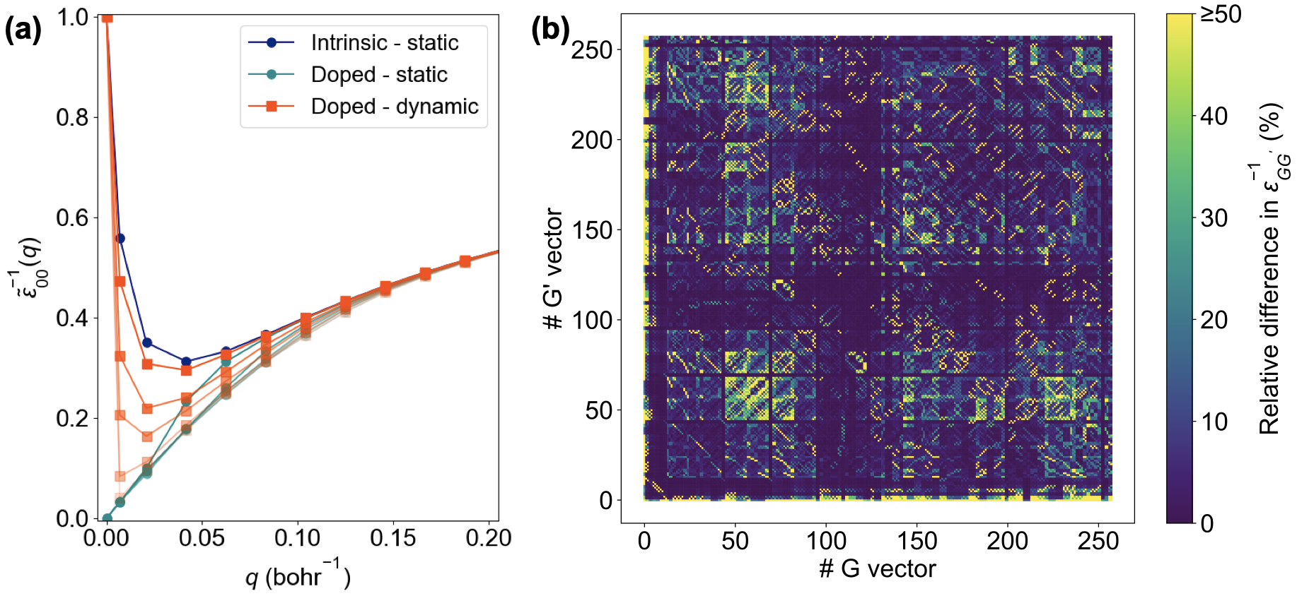
While previous GW-BSE calculations of carrier-doped TMD monolayers assumed that only the head matrix element was strongly modified with doping 17, 18, we find significant differences between the matrix elements of a doped and intrinsic MoTe2 monolayer for several and combinations. In Figure 2b, we show, for all and combinations, the relative variation in the static matrix elements , for a wavevector bohr-1. While the largest absolute difference is indeed found for the head matrix element (), we find non-negligible contributions from carrier screening to all matrix elements, ultimately giving rise to local-field effects and highlighting the importance of going beyond the spatially uniform screening background approximation when modeling the carrier screening in doped low-dimensional systems (Figure 1cd).
Next, we use our new PPM to obtain the frequency-dependent dielectric matrix of a doped monolayer MoTe2 for six different doping densities. The inverse dielectric matrix is then used to compute the screened Coulomb interaction (Eq. 1), used itself to obtain the QP energies, within the GW approximation.
Solving the BSE with the fully frequency-dependent dielectric matrix with the form of Eq. 4 is impractical, and a PPM can greatly reduce computational complexity without loss of accuracy. Assuming that the carrier plasmon-pole dominates the low-frequency screening and that the exciton is well-localized in -space, such that , where can be approximated as the exciton binding energy , Eq. 4 can be simplified to
| (8) |
with
| (9) |
where and are defined in Eqs. 6 and 7, respectively, and the exciton binding energy is self-consistently computed. This expression only requires calculation of the intrinsic and doped static dielectric matrix, a considerable simplification and storage memory reduction relative to treating the full-frequency dielectric matrix.
The head () of the inverse effective dielectric matrix for doped monolayer MoTe2 evaluated at is depicted in Figure 2a, revealing noticeable deviations from the static case, with a sharp increase to unity as . Such behavior is accurately described only when the effective inverse dielectric function is computed self-consistently, as shown in Figure S4. This sharp increase to unity is consistent with the carrier plasmon pole frequency tending to zero for very long wavelength (), hence removing any screening contribution from the charged free carriers.
Next, the effective dynamical dielectric matrix defined in Eq. 89 is used to solve the BSE and compute the excited state properties of a doped monolayer MoTe2. There is a limited number of works that have investigated the electronic and optical properties of monolayer 2H MoTe2 5, 46, 47, 48, 49, 50, whose structure is shown in Figure 3ab. Moreover, a spread of QP gap values are reported in prior computational studies, which reflect either an insufficient level of theory or a lack of convergence, as pointed our in Ref. 29, further motivating our calculations.
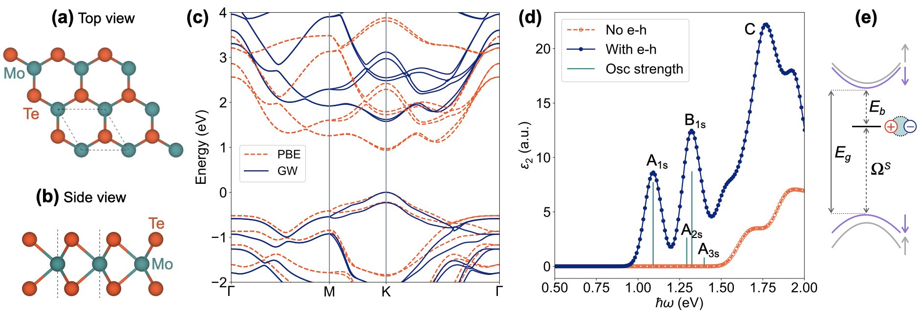
Here, we compute the QP band structure within the GW approximation (Figure 3c), and report a direct gap at of eV ( eV) with (without) spin-orbit coupling (SOC). Compared with other Mo-based monolayer TMDs, MoTe2 has a stronger SOC which splits the valence band maximum (VBM) by meV and the conduction band minimum (CBM) by meV, at the point of the Brillouin zone 50.
The presence of strongly bound excitons in MoTe2 explains the large difference between the QP gap and the measured optical gap of eV 28, 46. Indeed, for 2D TMDs, the photoluminescence spectrum is dominated by exciton transitions, rather than band-to-band recombination (Figure 3e) 6. The imaginary part of the frequency-dependent dielectric function , obtained from a GW-BSE calculation assuming incident light polarized in the plane of the monolayer, is displayed in Figure 3d. As expected, the inclusion of electron-hole interactions leads to good agreement with the experimental optical gap of eV 28, 46. The spin-orbit splitting of the VBM and CBM, depicted in Figure 3e, leads to two distinct exciton series, with the and exciton peak, respectively, at eV and eV. Transitions associated with the and states of the excitons are included under this second peak, and fall at an energy of and eV, respectively. Relevant results for the exciton states are reported in Table 1 and are in very good agreement with energies obtained from our photoluminescence measurements, which are detailed elsewhere (Ref. 28). The slight remaining discrepancy is likely due to the dielectric environment, i.e., hBN substrate, present in the experimental setup and not considered in the calculations. Computational parameters are reported in the SI.
| Excited | BSE | EXP 28 | ||
|---|---|---|---|---|
| states | (eV) | (meV) | Dip. Mom. (a.u.) | (eV) |
The presence of charged free carriers significantly affects both the electronic and optical properties of 2D semiconductors, as it strongly modifies the electric background of the monolayer. As a result of two competing effects, a weakening of the electron-electron interaction and a decrease in the carrier-occupation energy 17, we observe a large renormalization of the QP gap with increasing doping density (Figure 4a). At relatively low carrier density, the gap drops sharply from eV down to eV at a carrier density of cm-2, eventually reaching eV at a higher carrier density of cm-2. At even higher doping concentration, the QP gap is expected to increase, due to the Burstein-Moss shift of the continuum energy 51, 52 as free carriers populate the conduction band. Our PPM works remarkably well to predict the band gap renormalization, with a maximal deviation of 17 meV with respect to a FF calculation performed within the static subspace approximation. Figure 4a also highlights the underestimation in the screening when assuming that only the head of the dielectric function is modified by the presence of free carriers; the use of a single plasmon pole 18 overestimates the screening and, hence, the QP gap renormalization (Figure S5a).
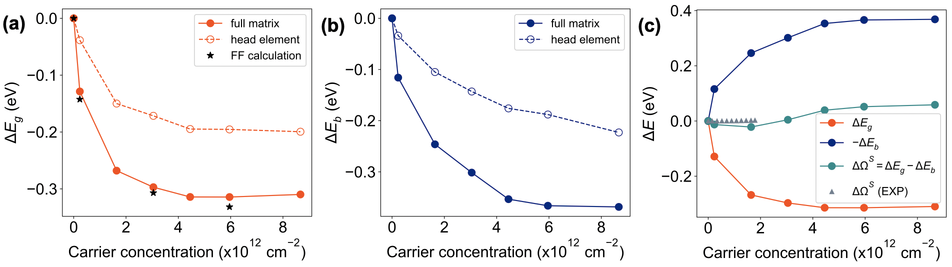
Excitonic and optical properties, including exciton binding energy, exciton energy, and oscillator strength, are also altered by the presence of charged free carriers, as shown in Figures 4 and 5. As expected from the carrier-induced screening of the electron-hole Coulomb interaction combined with Pauli blocking effects that prevent direct vertical transitions at the valley (Figure 5), the exciton binding energy decreases with doping, by as much as meV at a doping density of cm-2, and eventually saturates at higher carrier concentration. Figure 4b also shows that restricting inclusion of dynamical effects from carrier plasmon screening to the head matrix element (instead of the full matrix) leads to a much smaller reduction in exciton binding energy, highlighting the importance of off-diagonal matrix elements and, hence, local-field effects. In contrast, a static calculation clearly overestimates the screening for free carriers and so does a single plasmon-pole approach 18, as reported in Figure S5b. Notably, omitting to self-consistently (SC) compute the exciton binding energy in Eq. 9 underestimates both the screening and reduction in exciton binding energy with increasing doping (Figure S4 and S5b).
The reduction in exciton binding energy almost exactly compensates for the renormalization of the QP gap, resulting in an almost constant exciton energy with doping density. This is shown in Figure 4c, which also validates the efficiency of our PPM, as the theoretical results are in good qualitative and quantitative agreement with photoluminescence data reported in Ref. 28, in the experimentally-accessible doping region. The corresponding computed absorption spectra can be found in Figure S7. A similar conclusion for a doped MoS2 monolayer was reported in a prior work 18, with a more approximate treatment of the dynamical screening associated with the free carriers, as emphasized in Figure S4c. Here, we go beyond these approximations and obtain good agreement with experiments for the exciton energy, and quantitative predictions for QP band gap, as verified with a FF calculation.
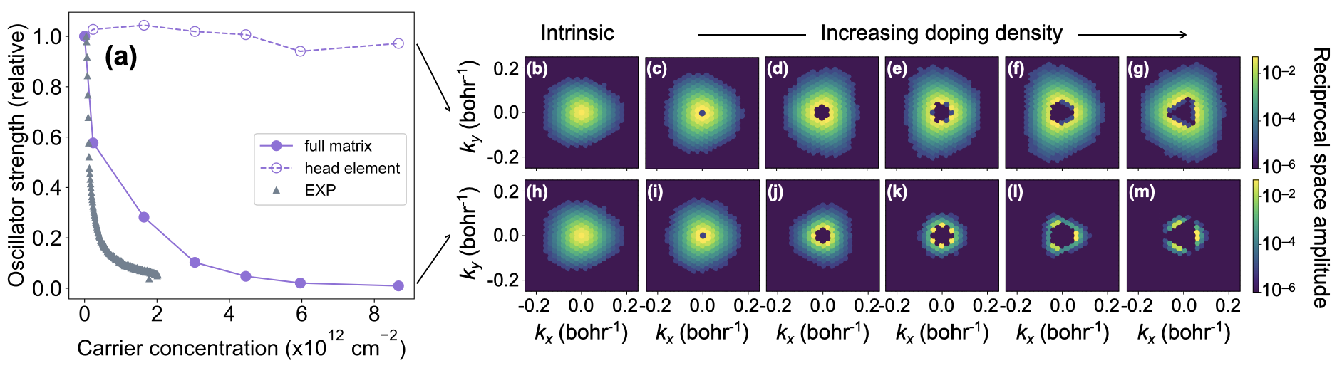
Figure 5a shows the change in oscillator strength for the first exciton, relative to the intrinsic system, compared to experimental data obtained for a carrier-doped MoTe2 monolayer 28. A decrease in oscillator strength with increasing doping density is observed and can be explained as originating from two effects: Pauli blocking and delocalization of the exciton in real space, due to a weakening of the electron-hole interaction from carrier screening. The latter is further verified by plotting the exciton wavefunction, shown at various doping densities in Figure 5hm; the exciton becomes more localized in -space, corresponding to a delocalization in real-space. Since optical absorption occurs when the electron and hole positions are identical, the probability for absorption is reduced as the exciton delocalizes, explaining the reduced oscillator strength. The importance of solving the BSE self-consistently for the doped systems is evidenced from Figure S6. Moreover, while neglecting local-field effects leads to an incorrect doping-dependence of the oscillator strength and exciton wavefunction (Figure 5bg), our modified PPM shows remarkable agreement with photoluminescence peak intensity at low doping density.
In conclusion, we have developed a new, computationally-efficient approach to predict the electronic and optical properties of doped semiconductors within the ab initio GW-BSE framework, and we have applied it to monolayer MoTe2, a 2D material of significant interest and compared it to detailed spectroscopy experiments 28. We find that as a function of carrier density, the band gap renormalization and the reduction of the exciton binding energy have a similar doping dependence, resulting in an almost constant exciton energy for the lowest excited state. This is in agreement with recent photoluminescence measurements where the onset of the optical spectrum remains unchanged with increased doping density. This agreement is made possible by careful treatment of the dynamical effects in the effective screened electron-hole interaction, accounting for the off-diagonal terms responsible for local-field effects. As our new PPM can further be applied to treat the charge carrier screening in any 2D material with delocalized excitons or van der Waals homobilayer, we expect it will deepen our understanding of the underlying physics in realistic intrinsically doped 2D devices.
The Supporting Information is available free of charge.
-
•
Ab initio calculations parameters; effective 2D dielectric function; parametrization, performance, and efficiency of the PPM; absorption spectra for doped MoTe2 monolayers (PDF).
The calculations in this work were primarily supported by the Center for Computational Study of Excited-state Phenomena in Energy Materials (C2SEPEM), funded by the US Department of Energy (DOE) under contracts No. DE-AC02-05CH11231 and DE-FG02-07ER46405. The Theory of Materials FWP at LBNL, funded by the DOE under contract No. DE-AC02-05CH11231, supported the development of the plasmon-pole model. Computational resources are provided by the National Energy Research Scientific Computing Center (NERSC). A.C acknowledges the support from Wallonie Bruxelles International under contract No. SUB/2021/512815.
References
- Keldysh 1979 Keldysh, L. V. Coulomb interaction in thin semiconductor and semimetal films. Soviet Journal of Experimental and Theoretical Physics Letters 1979, 29, 658
- Splendiani et al. 2010 Splendiani, A.; Sun, L.; Zhang, Y.; Li, T.; Kim, J.; Chim, C.-Y.; Galli, G.; Wang, F. Emerging photoluminescence in monolayer MoS2. Nano Letters 2010, 10, 1271–1275
- Mak et al. 2013 Mak, K. F.; He, K.; Lee, C.; Lee, G. H.; Hone, J.; Heinz, T. F.; Shan, J. Tightly bound trions in monolayer MoS2. Nature Materials 2013, 12, 207–211
- Thygesen 2017 Thygesen, K. S. Calculating excitons, plasmons, and quasiparticles in 2D materials and van der Waals heterostructures. 2D Materials 2017, 4, 022004
- Ramasubramaniam 2012 Ramasubramaniam, A. Large excitonic effects in monolayers of molybdenum and tungsten dichalcogenides. Phys. Rev. B 2012, 86, 115409
- Qiu et al. 2013 Qiu, D. Y.; da Jornada, F. H.; Louie, S. G. Optical spectrum of MoS2: Many-body effects and diversity of exciton states. Phys. Rev. Lett. 2013, 111, 216805
- Chernikov et al. 2014 Chernikov, A.; Berkelbach, T. C.; Hill, H. M.; Rigosi, A.; Li, Y.; Aslan, O. B.; Reichman, D. R.; Hybertsen, M. S.; Heinz, T. F. Exciton binding energy and nonhydrogenic Rydberg series in monolayer WS2. Phys. Rev. Lett. 2014, 113, 076802
- Ye et al. 2014 Ye, Z.; Cao, T.; O’Brien, K.; Zhu, H.; Yin, X.; Wang, Y.; Louie, S. G.; Zhang, X. Probing excitonic dark states in single-layer tungsten disulphide. Nature 2014, 513, 214–218
- Ugeda et al. 2014 Ugeda, M. M.; Bradley, A. J.; Shi, S.-F.; da Jornada, F. H.; Zhang, Y.; Qiu, D. Y.; Ruan, W.; Mo, S.-K.; Hussain, Z.; Shen, Z.-X.; Wang, F.; Louie, S. G.; Crommie, M. F. Giant bandgap renormalization and excitonic effects in a monolayer transition metal dichalcogenide semiconductor. Nature Materials 2014, 13, 1091–1095
- He et al. 2014 He, K.; Kumar, N.; Zhao, L.; Wang, Z.; Mak, K. F.; Zhao, H.; Shan, J. Tightly bound excitons in monolayer WSe2. Phys. Rev. Lett. 2014, 113, 026803
- Wang et al. 2015 Wang, G.; Marie, X.; Gerber, I.; Amand, T.; Lagarde, D.; Bouet, L.; Vidal, M.; Balocchi, A.; Urbaszek, B. Giant enhancement of the optical second-harmonic emission of WSe2 monolayers by laser excitation at exciton resonances. Phys. Rev. Lett. 2015, 114, 097403
- Mak et al. 2012 Mak, K. F.; He, K.; Shan, J.; Heinz, T. F. Control of valley polarization in monolayer MoS2 by optical helicity. Nature Communications 2012, 7, 494–498
- Ross et al. 2013 Ross, J. S.; Wu, S.; Yu, H.; Ghimire, N. J.; Jones, A. M.; Aivazian, G.; Yan, J.; Mandrus, D. G.; Xiao, D.; Yao, W.; Xu, X. Electrical control of neutral and charged excitons in a monolayer semiconductor. Nature Communications 2013, 4, 1474
- Hüser et al. 2013 Hüser, F.; Olsen, T.; Thygesen, K. S. Quasiparticle GW calculations for solids, molecules, and two-dimensional materials. Phys. Rev. B 2013, 87, 235132
- Plechinger et al. 2015 Plechinger, G.; Nagler, P.; Kraus, J.; Paradiso, N.; Strunk, C.; Schuller, C.; Korn, T. Identification of excitons, trions and biexcitons in single-layer WS2. Rapid Research Letter 2015, 9, 457–461
- Shang et al. 2015 Shang, J.; Shen, X.; Cong, C.; Peimyoo, N.; Cao, B.; Eginligil, M.; Yu, T. Observation of excitonic fine structure in a 2D transition-metal dichalcogenide semiconductor. ACS Nano 2015, 9, 647–655
- Liang and Yang 2015 Liang, Y.; Yang, L. Carrier plasmon induced nonlinear band gap renormalization in two-dimensional semiconductors. Phys. Rev. Lett. 2015, 114, 063001
- Gao et al. 2016 Gao, S.; Liang, Y.; Spataru, C. D.; Yang, L. Dynamical excitonic effects in doped two-dimensional semiconductors. Nano Letters 2016, 16, 5568–5573
- Radisavljevic et al. 2011 Radisavljevic, B.; Radenovic, A.; Brivio, J.; Giacometti, V.; Kis, A. Single-layer MoS2 transistors. Nature Nanotechnology 2011, 6, 147–150
- Radisavljevic and Kis 2013 Radisavljevic, B.; Kis, A. Mobility engineering and a metal–insulator transition in monolayer MoS2. Nature Materials 2013, 12, 815–820
- Mouri et al. 2013 Mouri, S.; Miyauchi, Y.; Matsuda, K. Tunable photoluminescence of monolayer MoS2 via chemical doping. Nano Letters 2013, 13, 5944–5948
- Hedin 1965 Hedin, L. New method for calculating the one-particle Green’s function with application to the electron-gas problem. Phys. Rev. 1965, 139, A796–A823
- Strinati et al. 1982 Strinati, G.; Mattausch, H. J.; Hanke, W. Dynamical aspects of correlation corrections in a covalent crystal. Phys. Rev. B 1982, 25, 2867–2888
- Hybertsen and Louie 1986 Hybertsen, M. S.; Louie, S. G. Electron correlation in semiconductors and insulators: Band gaps and quasiparticle energies. Phys. Rev. B 1986, 34, 5390–5413
- Rohlfing and Louie 2000 Rohlfing, M.; Louie, S. G. Electron-hole excitations and optical spectra from first principles. Phys. Rev. B 2000, 62, 4927–4944
- Godby and Needs 1989 Godby, R. W.; Needs, R. J. Metal-insulator transition in Kohn-Sham theory and quasiparticle theory. Phys. Rev. Lett. 1989, 62, 1169–1172
- Oschlies et al. 1995 Oschlies, A.; Godby, R. W.; Needs, R. J. GW self-energy calculations of carrier-induced band-gap narrowing in n-type silicon. Phys. Rev. B 1995, 51, 1527–1535
- Biswas et al. 2023 Biswas, S.; Champagne, A.; Haber, J. B.; Pokawanvit, S.; Wong, J.; Akbari, H.; Krylyuk, S.; Watanabe, K.; Taniguchi, T.; Davydov, A. V.; Balushi, Z. Y. A.; Qiu, D. Y.; da Jornada, F. H.; Neaton, J. B.; Atwater, H. A. Rydberg excitons and trions in monolayer MoTe2. 2023; http://arxiv.org/abs/2302.03720, arXiv:2302.03720 [cond-mat, physics:physics]
- Qiu et al. 2016 Qiu, D. Y.; da Jornada, F. H.; Louie, S. G. Screening and many-body effects in two-dimensional crystals: Monolayer MoS2. Phys. Rev. B 2016, 93, 235435
- Hybertsen and Louie 1987 Hybertsen, M. S.; Louie, S. G. Ab initio static dielectric matrices from the density-functional approach. I. Formulation and application to semiconductors and insulators. Phys. Rev. B 1987, 35, 5585–5601
- Nguyen et al. 2012 Nguyen, H.-V.; Pham, T. A.; Rocca, D.; Galli, G. Improving accuracy and efficiency of calculations of photoemission spectra within the many-body perturbation theory. Phys. Rev. B 2012, 85, 081101
- Del Ben et al. 2019 Del Ben, M.; da Jornada, F. H.; Antonius, G.; Rangel, T.; Louie, S. G.; Deslippe, J.; Canning, A. Static subspace approximation for the evaluation of quasiparticle energies within a sum-over-bands approach. Phys. Rev. B 2019, 99, 125128
- Shao et al. 2016 Shao, M.; Lin, L.; Yang, C.; Liu, F.; Da Jornada, F. H.; Deslippe, J.; Louie, S. G. Low rank approximation in calculations. Science China Mathematics 2016, 59, 1593–1612
- Ando et al. 1982 Ando, T.; Fowler, A. B.; Stern, F. Electronic properties of two-dimensional systems. Rev. Mod. Phys. 1982, 54, 437–672
- Das Sarma and Hwang 1996 Das Sarma, S.; Hwang, E. H. Dynamical response of a one-dimensional quantum-wire electron system. Phys. Rev. B 1996, 54, 1936–1946
- Spataru and Léonard 2010 Spataru, C. D.; Léonard, F. Tunable band gaps and excitons in doped semiconducting carbon nanotubes made possible by acoustic plasmons. Phys. Rev. Lett. 2010, 104, 177402
- Spataru and Léonard 2013 Spataru, C. D.; Léonard, F. Quasiparticle and exciton renormalization effects in electrostatically doped semiconducting carbon nanotubes. Chemical Physics 2013, 413, 81–88
- Strinati 1984 Strinati, G. Effects of dynamical screening on resonances at inner-shell thresholds in semiconductors. Phys. Rev. B 1984, 29, 5718–5726
- Strinati 1988 Strinati, G. Application of the Green’s functions method to the study of the optical properties of semiconductors. Riv. Nuovo Cim. 1988, 11, 1–86
- Zhang et al. 2023 Zhang, X.; Leveillee, J. A.; Schleife, A. Effect of dynamical screening in the Bethe-Salpeter framework: Excitons in crystalline naphthalene. 2023; http://arxiv.org/abs/2302.07948, arXiv:2302.07948 [cond-mat]
- Lischner et al. 2013 Lischner, J.; Vigil-Fowler, D.; Louie, S. G. Physical origin of satellites in photoemission of doped graphene: An ab initio plus cumulant study. Phys. Rev. Lett. 2013, 110, 146801
- Zhou et al. 2015 Zhou, J. S.; Kas, J. J.; Sponza, L.; Reshetnyak, I.; Guzzo, M.; Giorgetti, C.; Gatti, M.; Sottile, F.; Rehr, J. J.; Reining, L. Dynamical effects in electron spectroscopy. The Journal of Chemical Physics 2015, 143, 184109
- Zhang et al. 1989 Zhang, S. B.; Tománek, D.; Cohen, M. L.; Louie, S. G.; Hybertsen, M. S. Evaluation of quasiparticle energies for semiconductors without inversion symmetry. Phys. Rev. B 1989, 40, 3162–3168
- Deslippe et al. 2012 Deslippe, J.; Samsonidze, G.; Strubbe, D. A.; Jain, M.; Cohen, M. L.; Louie, S. G. BerkeleyGW: A massively parallel computer package for the calculation of the quasiparticle and optical properties of materials and nanostructures. Computer Physics Communications 2012, 183, 1269–1289
- Ismail-Beigi 2006 Ismail-Beigi, S. Truncation of periodic image interactions for confined systems. Phys. Rev. B 2006, 73, 233103
- Ruppert et al. 2014 Ruppert, C.; Aslan, O. B.; Heinz, T. F. Optical properties and band gap of single- and few-Layer MoTe2 crystals. Nano Letters 2014, 14, 6231–6236
- Lezama et al. 2015 Lezama, I. G.; Arora, A.; Ubaldini, A.; Barreteau, C.; Giannini, E.; Potemski, M.; Morpurgo, A. F. Indirect-to-direct band gap crossover in few-layer MoTe2. Nano Letters 2015, 15, 2336–2342
- Yang et al. 2015 Yang, J.; Lü, T.; Myint, Y. W.; Pei, J.; Macdonald, D.; Zheng, J.-C.; Lu, Y. Robust excitons and trions in monolayer MoTe2. ACS Nano 2015, 9, 6603–6609
- Koirala et al. 2016 Koirala, S.; Mouri, S.; Miyauchi, Y.; Matsuda, K. Homogeneous linewidth broadening and exciton dephasing mechanism in MoTe2. Phys. Rev. B 2016, 93, 075411
- Robert et al. 2016 Robert, C.; Picard, R.; Lagarde, D.; Wang, G.; Echeverry, J. P.; Cadiz, F.; Renucci, P.; Högele, A.; Amand, T.; Marie, X.; Gerber, I. C.; Urbaszek, B. Excitonic properties of semiconducting monolayer and bilayer MoTe2. Phys. Rev. B 2016, 94, 155425
- Moss 1954 Moss, T. S. The interpretation of the properties of indium antimonide. Proceedings of the Physical Society. Section B 1954, 67, 775–782
- Burstein 1954 Burstein, E. Anomalous optical absorption limit in InSb. Phys. Rev. 1954, 93, 632–633
