Wafer-scale method for amorphizing superconducting thin films
Abstract
We demonstrate ion irradiation as a wafer-scale method for the fabrication of amorphous superconducting thin films. We explore irradiation using argon and gallium ions on single-element and compound materials. Our results indicate that both ions increase disorder in the atomic structure in a qualitatively similar manner, i.e., they destroy the grain structure, increase resistivity and alter the superconducting transition temperature. However, argon irradiation tends to yield gas pockets that can be detrimental for applications. We show that gallium irradiation allows to produce a thin, uniform, and amorphous molybdenum silicide film that is promising, e.g., for superconducting nanowire single-photon detectors.
I Introduction
Nanoscale superconducting structures allow both new functionalities [1, 2, 3, 4, 5] and opportunities for improving the packaging density and scaling up quantum technologies [6]. Typical superconducting devices are fabricated from polycrystalline thin films, such as sputter deposited Nb or evaporated Al. However, the geometries of nanostructures become irreproducible when their critical dimensions approach the grain size of the material. One promising way to solve this problem is to use novel, single-crystalline two-dimensional superconductors [7, 8] whose processing, however, is not sufficiently mature to allow large-scale fabrication. Here we study an opposite approach to improve reproducibility: decreasing the grain size, ultimately down to that of an amorphous material.
Increase of atomic disorder typically enhances the normal-state resistivity which, at nanoscale thickness, enables films with high sheet resistance and kinetic inductance in the normal and superconducting states, respectively. Here, is the Planck constant and is the superconducting energy gap. These properties allow, e.g., compact superinductors based on high for quantum information processing [9, 10], quantum phase slip (QPS) devices for quantum metrology [3, 4, 5], and superconducting nanowire single-photon detectors (SNSPD) for quantum communication [1, 2]. Typical may span roughly 1–4 for superinductors or QPS and 100–200 for SNSPDs. These ranges should be compared to the limit in which superconductivity is destroyed by fluctuations: k [11, 12] where is the quantum resistance of Cooper pairs and is the elementary charge.
Because conventional superconductivity arises from the interplay between electrons and lattice, it is expected that the increase of disorder may affect the critical temperature , but the direction of the change is less obvious. Already since the 1950s, several studies on single-element materials, e.g., Al, W, Ga, and Mo, have demonstrated an increase of when the growth of large grains has been prevented, e.g., by evaporating on a cold substrate or in the presence of oxygen, or by creating a layered structure with other materials [13, 14, 15, 16, 17, 11]. Evaporating with oxygen is a key fabrication step for the modern superinductors based on granular aluminium [9, 10]. In contrast, applying neutron irradiation to increase disorder in several high- compounds with an -15 lattice yields a dramatic decrease of [18]. Other examples of the subtle interplay between disorder and superconductivity include, e.g., the dependence of on the crystalline phase of tantalum [19], and that proton irradiation decreases , but increases the upper critical field of Nb [20].
The disordered structure is unstable in many single-element materials, and already room temperature conditions are sufficient to crystallize the material into relatively large grains. Disorder can be stabilized, e.g., with oxidized grain surfaces or with alloyed compounds, which may already be of interest in terms of increased [21].
One such compound with a metastable disordered phase is MoSi, which is a well-known material for SNSPDs and can be fabricated by, e.g, sputtering from an alloy-target to a cooled substrate [22] or by co-sputtering at room temperature [23, 24]. In the referred experiments, the optimal stoichiometry was found to be about 80% Mo and 20% Si, as a result of a trade-off between maintaining the stability of an amorphous phase, which requires Si, and maximizing , which would favour pure electron-dense amorphous Mo. Other methods for fabricating disordered MoSi and other silicides include mixing a deposited metal film into a silicon substrate by ion irradiation [25] or by annealing, a technique that was used in the observation of QPS [26]. Recently, it was shown that focused ion beam (FIB) irradiation by gallium or helium ions increases the disorder, , and of MoSi formed by thermal annealing [27]. The FIB method is a relatively slow direct-writing process, with time consumption that scales linearly with the processed area.
In this article, we explore ion irradiation as a wafer-scale process for increasing disorder in superconducting thin films with high throughput and reproducibility. We study both single-element materials and compounds in two common groups of superconductors: nitrides and silicides. The films studied in this paper have been fabricated by sputtering, which typically yields polycrystalline films. In the present work, our focus is two-fold: (i) tentative testing for a wide range of materials and (ii) systematically investigating MoSi, which has shown promising results under local irradiation treatment [27].
II Materials and methods
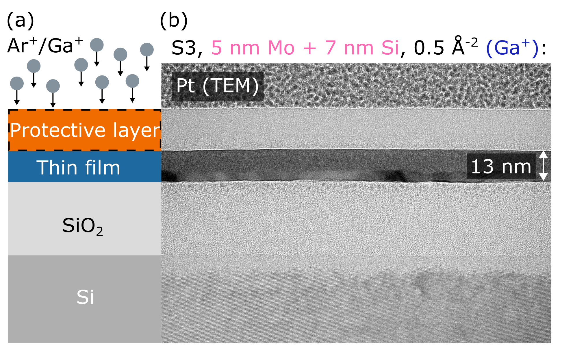
Figure 1 illustrates the wafer structure and ion implantantion treatment and shows the corresponding transmission electron microscope (TEM) image of a MoSi wafer which was taken after the ion irradiation treatment. The thin films were sputtered on top of a silicon wafer terminated by a silicon dioxide layer. A dielectric layer was added on top of some of the wafers to protect the superconducting film from, e.g., oxidation. The wafers were irradiated with argon or gallium ions. As a noble gas, argon should irradiate without any doping of the superconducting film. On the other hand, gallium had provided promising results in Ref. [27] without any evidence of doping problems.
We used Monte Carlo simulations (not shown) to choose an acceleration voltage for each wafer that is expected to maximize the fraction of kinetic energy deposited into the superconduting film. Therefore, also the majority of the irradiation ions are deposited into the film. We report the irradiation fluences in units of Å cm-2, which roughly corresponds to the number of ions deposited on the area of a single atom. It also yields a rough estimate for the percentage of impurity atoms deposited into the superconducting film, since our films of about have the thickness of the order of 100 atoms.
| Material | Thickness (nm) | Protective layer | Ion |
| Single-elements | |||
| Al | none | ||
| V | – | none | |
| Nb | Al2O3/none | ||
| Nitrides | |||
| TiN | Al2O3/none | ||
| NbN | Al2O3/none | ||
| Silicides | |||
| MoSi (M-series) | SiO2/Al2O3 | / | |
| MoSi (S-series) | Al2O3 | / | |
| MoSi (S-series) | Al2O3 | / | |
Table 1 provides an overview of the thin film materials, their targeted sputtering thicknesses, protective layers, and the ions of the irradiation treatment. We studied 3 single-element materials (Al, V, and Nb), 2 nitrides (TiN and NbN), and 1 silicide (MoSi). For MoSi, we performed a study of the effect of ion fluence for Mo-rich stoichiometry (M-series wafers), and a smaller number of process variants for Si-rich stoichiometry (S-series).
Nitrides were deposited by reactive sputtering of Nb or Ti in a flow of argon and nitrogen. For TiN, we used a recipe that typically produces . For NbN, the maximum of is obtained with 1:1 stoichiometry [28], but in this work, we intentionally used two higher nitrogen flow values to increase and decrease to about 8 K or 6 K, respectively. For MoSi films, first a layer of molybdenum and then a layer of silicon was deposited, which allowed tuning the stoichiometry by changing the ratio of the film thicknesses. The thickness estimates are based on longer depositions using the same sputtering parameters, and measuring the resulting thicker films. However, the short deposition times of thin films yield a significant uncertainty of the film thickness. We estimate the stoichiometries of about 65% Mo + 35% Si, 48% Mo + 52% Si, and 35% Mo + 65% Si for our film variants with , , and of Mo (and of Si), respectively.
We experimented with two types of protective dielectric films: SiO2 grown by plasma enhanced chemical vapor deposition (PECVD) or of Al2O3 grown by atomic layer deposition (ALD). The MoSi compounds were formed by annealing in nitrogen environment at for minutes after the deposition of the protective layer. Other materials were not annealed. After thin film fabrication, the wafers went through a wafer-scale broad beam ion irradiation treatment. We varied the ion fluence to observe potential progressive effects of irradiation and used higher fluences when using argon ions because their impact is smaller due to the smaller atomic weight. The protective layers were deposited on many wafers at a time significantly after sputtering the superconducting films, which exposed the superconducting films for native oxide growth before the protection, but not during the irradiation process.
In total, we produced 46 irradiated wafers and measured their at room temperature. Most of the films were also imaged with a scanning electron microscope (SEM). We used data from this fast characterization to select an illustrative set of samples for the more elaborate cryogenic characterization (presented in Sec. IV). Based on all these data, a set of 9 films were selected for TEM imaging (Sec. III): NbN with and without protective layer, identical MoSi films with varied ion fluence, films that seemed visually defective in SEM, MoSi with highest Tc, and MoSi films that were promising in all of the initial measurements.
III Imaging
Figure 2(a) shows the TEM image of a Mo-poor MoSi film irradiated with argon, which yielded the highest K of all our MoSi films (see Sec. IV below). There are gas pockets both in the substrate and protective layer, which deform and alter the thickness of the MoSi film. The energy-dispersive X-ray spectroscopy (EDS) data (not shown) relate the gas pockets to argon. The film is continuous, with grains not resolvable with TEM. Fast Fourier transform (FFT) analysis shows a broad ring at 0.23 nm/cycle. This suggests that the film is amorphous with short-range order.
Figures 2(b–d) show TEM images of Mo-rich MoSi films treated with an increasing fluence of ions. The films are heterogeneous and have a bilayer structure, with a polycrystalline bottom and an amorphous top layer. Inset of FFT analysis of the bottom layer confirms the crystallinity of the grains. Inset of EDS data indicates that the bottom layer consists mostly of molybdenum whereas the top layer is a MoSi alloy. Higher fluences of gallium result in less heterogeneous films.
Figure 1(b) shows the TEM image of Mo-poor film (S3) with of Mo. The image shows a bilayer structure, similarly as for the Mo-rich films (Fig. 2(b–c)).
Figures 2(e–f) show TEM images of Mo-poor MoSi films (S1–S2) with of Mo. The thinner layer of molybdenum yields a better intermixing with the silicon top layer (compare Fig. 1(b) and Fig. 2(e)). Further increasing the gallium fluence to 1.0 Å-2 leads to a continuous, homogeneous film of molybdenum and silicon, without resolvable grains by TEM. The FFT analysis shows a broad ring at 0.23 nm/cycle, suggesting that the film is amorphous with short-range order.
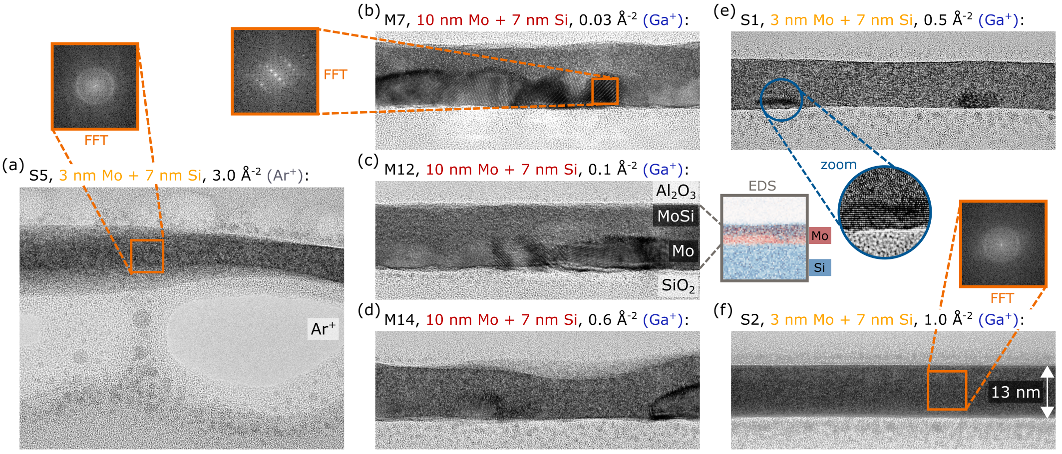
Figure 2 indicates that our annealing process did not result in complete mixing of Mo and Si especially for the Mo-rich stoichiometries. This problem could be overcome, for example, by sputtering from a MoSi compound target or by cosputtering [22, 23, 24]. Ion irradiation improves mixing, but its efficiency is expected to depend on the fact that the irradiation atoms yield the largest impact on atoms with a roughly similar atomic mass. For Ga+ (70 u), the order of our Mo and Si layers is non-optimal, since the ions should be more effective at driving Mo atoms (96 u) into the substrate than Si atoms (28 u) into the Mo layer. On the other hand, Ar+ (40 u) is a closer match to Si.
Figures 3(a–b) show the TEM images of NbN films without and with an Al2O3 protective layer (films NbN5–NbN6), respectively. Both films were irradiated with the same fluence of argon. The film with a protective layer (NbN6) shows rotated domains and polycrystalline grains. There are well-defined peaks over a diffuse background in FFT analysis performed on the area highlighted with orange square. The unprotected film (NbN5) shows a thin amorphized layer over polycrystalline NbN (see FFT and zoom insets). However, the amorphization of the top-most layer may also result from the deposition of platinum instead of the original irradiation process.
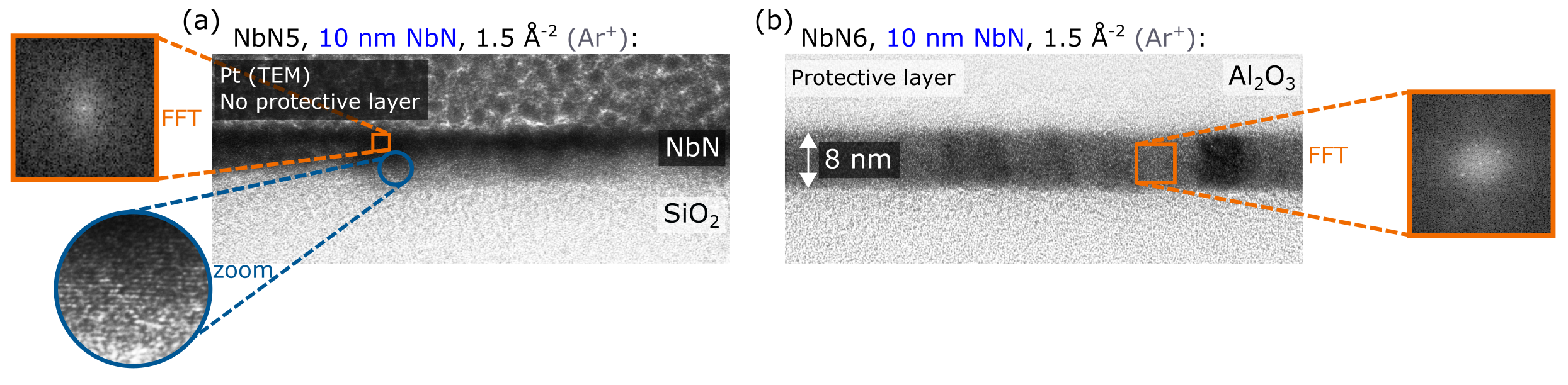
While irradiation seemed to yield detrimental gas pockets into the substrate of MoSi films, it did not into that of NbN films. One potential explanation is in the higher fluence of film S5 (3 Å-2) than our NbN films (1.5 Å-2), but the acceleration voltage has an effect on both the required fluence and the stopping range of the implanted ions. The present amount of data does not rule out the use of ions for irradiation, but it would also be interesting to explore noble gases with higher atomic masses.
IV Sheet resistance and critical temperature
We measured the room temperature sheet resistance with a wafer-scale prober. For cryogenic measurements, we cleaved the wafers into small chips that were fully covered with the film on the top surface. The relative temperature dependence of down to the base temperature of 0.3 K of our cryostat is recorded through 4-probe measurements. Combining these data sets yields sheet resistance as a function of temperature . Figure 4 shows cryogenic measurements of MoSi, Nb and NbN films that provide data for and . The most relevant data is collated into Table 2, which excludes V and TiN that were not superconducting in our experiments.

| Label | Material | Prot. | Ion | Fluence (Å-2) | / | (K) | |||
| M1 | Mo Si | SiO2 | 1 | – | 115 | – | 120 | 4.8 | |
| M7 | Mo Si | Al2O3 | 0.03 | – | 48 | – | 43 | 4.0 | |
| M12 | Mo Si | Al2O3 | 0.1 | – | 71 | – | 69 | 4.3 | |
| M14 | Mo Si | Al2O3 | 0.6 | – | 105 | – | 109 | 4.8 | |
| S1 | Mo Si | Al2O3 | 0.5 | – | 166 | – | 176 | 5.0 | |
| S2 | Mo Si | Al2O3 | 1 | – | 177 | – | 188 | 4.9 | |
| S3 | Mo Si | Al2O3 | 0.5 | – | 169 | – | 177 | 4.1 | |
| S5 | Mo Si | Al2O3 | 3 | – | 177 | – | 187 | 5.7 | |
| NbN3 | NbN | none | 1.5 | 474 | 2080 | 4.4 | 3340 | 2.5 | |
| NbN5 | NbN | none | 1.5 | 535 | 2960 | 5.5 | 4760 | 2.4 | |
| NbN6 | NbN | Al2O3 | 1.5 | 530 | 1220 | 2.3 | 2200 | 1.9 | |
| NbN7 | NbN | none | 1.5 | 694 | 5090 | 7.3 | – | – | |
| NbN8 | NbN | Al2O3 | 1.5 | 694 | 1550 | 2.2 | – | – | |
| Nb1 | Nb | none | 0.5 | 13 | 30 | 2.3 | 21 | 4.7 | |
| Nb2 | Nb | Al2O3 | 0.5 | 13 | 40 | 3.0 | 33 | 2.9 | |
| Nb3 | Nb | none | 1.5 | 13 | 71 | 5.7 | 68 | 1.7 | |
| Nb4 | Nb | Al2O3 | 1.5 | 13 | 64 | 5.0 | 63 | 1.6 | |
| Al1 | Al | none | 1.5 | 3 | 25 | 9.5 | 19 | 1.7 |
In the MoSi films of Fig. 4, the resistance of Mo-rich films containing a layer of polycrystalline Mo decreases slightly when cooled down from room temperature toward . Film M14 had only separate spots of Mo and the resistance increases slightly when cooled down. In addition, there is a slight increase of for the most disordered films (S2 and S5, Mo-poor MoSi). The most disordered films also have the highest at 300 K. A similar trend can be observed for Nb: The of the most disordered film Nb4 (highest ) is constant above whereas of the less disordered Nb films decreases at low temperatures. The NbN films, which are the most resistive of our wafers, become even more resistive at low temperatures before a broad transition into the superconducting state, but the low-temperature increase of is larger for film NbN6 that is less disordered than NbN5.
The main trend in Table 2 is that the ion irradiation process and a higher ion fluence generally increase . For NbN, there is a significant difference in also between films with and without a protective layer, which is in agreement with Fig. 3.
Increasing disorder correlates with the increased of Al and MoSi. For MoSi, however, the interpretation of the results is less straightforward, since most of the films are not homogeneous. The increase of ion fluence also reduces the amount of polycrystalline Mo, which may affect the of the MoSi layer through the promiximity effect. The highest in MoSi, 5.7 K, was obtained for film S5, which is a Mo-poor film irradiated by ions.
In the case of Nb and NbN, the increase of disorder correlates with decreased . In TiN and V, we were not able to observe superconductivity at and above . We studied Nb, NbN, and TiN samples both with and without protective layers, and therefore the effect is not likely due to oxidation during the irradiation process. Vanadium did not have any protective layer, and it is not clear whether the lack of superconductivity was due to oxidation, impurities or disorder.
One of the limitations of our technique is that it requires a stable disordered phase, whereas some materials, including Al, tend to grow grains already at room temperature [15]. Our experiments on aluminium increased up to 1.7 K compared to the bulk value of about 1.2 K and to a reference value of about 1.4 K for 14 nm film deposited on a room temperature substrate [29]. There was no intended oxidation in our process, but as there was no protective layer, some oxidation of grain boundaries is possible.

Even small irradiation fluence in niobium seems to decrease , which makes the material less promising as a disordered superconductor. On the other hand, lithography-defined irradiation may allow Nb structures of different in the same layer. A significantly smaller decrease of , 0.16 K, has been observed in Nb films irradiated with protons [20], which was in agreement with theoretical calculations [31]. However, the proton-irradiated Nb films had an order of magnitude smaller resistivity than films Nb3–4.
One should also note that the protective layer of films Nb2 and Nb4 were fabricated after the deposition of the films as a separate step. Hence we cannot outrule in any of our Nb films the role of growth of native oxides, such as Nb2O5 that is known to have paramagnetic vacancies [32, 33]. Experiments on Nb have also reported a significant amount of quasiparticle states in the superconducting gap, which makes the material unsuitable for electronic cooling [34] and is associated with an anomalously high heat conductivity of the material [35]. Our results may contribute to these observations: If superconductivity in niobium is very sensitive to disorder, any defects in the material might locally suppress the superconductivity and introduce quasiparticle states in the material through the proximity effect.
Figure 5 illustrates our results on and . Figure 5(a) shows of M-series MoSi wafers as a function of ion fluence. As expected, increases as a function of fluence, but there is significant spread between several films with the same fluence. It is probable that the lowest resistance path in these films is through the Mo grains seen in Fig. 2.
Figure 5(b) shows of M- and S-series MoSi as a function of ion fluence. The values of are between and , and the highest values are obtained for the most disordered Mo-poor films. Films irradiated with argon have higher than those irradiated with gallium, but the present amount of data does not allow a definite conclusion. Our results indicate, though, that the potential doping of MoSi with does not explain the increase of , which is supported also by the small fluences, e.g., 1 Å-2 for our most promising MoSi film, labeled S2.
Figure 5(b) shows one film that had SiO2 as a protective dielectric (see Table 2, wafer M1). All other films in Fig. 5 have Al2O3 or no protective layer. However, several films similar to M1, protected with SiO2 and irradiated with the same fluence had reproducible values of between 98–120. The of wafer M1 is also the same as the highest measured from gallium-treated M-series films with Al2O3 layer. These results indicate that both materials, Al2O3 and SiO2, are suitable for the protective layer. Both layers can also be removed by selective etching.
Finally, Fig. 5(c) shows the relationship between and of MoSi, NbN, Nb, and Al wafers. We consider it as an application-oriented map into disordered superconductors, from which one could pick suitable materials for each purpose. Since ion irradiation is in principle suitable for increasing disorder of any superconducting thin film, future research on other materials may help to fill the empty parts of the map, e.g., in the regime . As examples of alternative techniques, tuning the oxidation of granular aluminium provides a wide range of at K [30], while reducing the thickness of ALD-grown NbN can provide values from about K and to K and k [28]. These value ranges of the alternative techniques are illustrated in Fig. 5(c) by the green and blue lines, respectively. Other interesting materials include, e.g., ALD-grown NbTiN [36].
V Conclusions and outlook
We present a wafer-scale method for the amorphization of superconducting thin films by using broad beam ion irradiation. Our treatment can be used independently of the material and its fabrication method. It would also be possible to obtain different levels of disorder in different areas of the same thin film by using lithography and, e.g., a thicker protective layer to block ion irradiation.
We use both gallium and argon ions and have studied various single-element (Al, V, Nb) and compound materials (NbN, TiN, MoSi), with the largest effort on MoSi films. Both ions increased the disorder and sheet resistance of the films, but in some cases, argon yielded gas pockets that may be detrimental for applications. As a result of disorder, the critical temperature increased in MoSi and Al, but decreased in TiN, NbN, and Nb. The critical temperature did not have significant dependence on the choice of ions, which indicates that the effect is not dominated by doping.
Both ions were used to produce a MoSi film that is amorphous with some short-range order. Our results show that relatively high can be achieved also with Mo-poor MoSi films (35% Mo, 65% Si), which was not expected based on literature [22, 23]. Our Mo-rich MoSi films had the tendency of forming a two-layer structure of polycrystalline Mo and amorphous MoSi. Further research on the effect of stoichiometry would benefit from better mixing of the material before ion irradiation, which could be achieved, e.g., through co-sputtering from Mo and Si targets or sputtering from a MoSi compound target. Such methods may also improve the uncertainty and reproducibility of the stoichiometry for nanoscale films.
The ion irradiation method enables tuning of and of superconducting thin films, potentially expanding the range of promising materials for different devices in quantum technology. In this work, we have demonstrated amorphous and uniform MoSi that is promising for superconducting nanowire single-photon detectors.
Acknowledgements.
We thank J. A. Sauls for useful discussions. For funding of our research project, we acknowledge the European Union’s Horizon 2020 Research and Innovation Programme under the Grant Agreement Nos. 862660/Quantum e-leaps, 899558/aCryComm, and 766853/EFINED. This project has also received funding from Business Finland through Quantum Technologies Industrial (QuTI) project No. 128291 and from Academy of Finland through Grant Nos. 310909 and 350220. This work was performed as part of the Academy of Finland Centre of Excellence program (project 336817 and 336819). We also acknowledge funding from an internal strategic innovation project of VTT related to the development of quantum computing technologies. This research was supported by the Scientific Service Units of IST Austria through resources provided by Electron Microscopy Facility. J. Senior acknowledges funding from the European Union’s Horizon 2020 Research and Innovation Programme under the Marie Skłodowska-Curie Grant Agreement No. 754411.References
- Gol’tsman et al. [2001] G. N. Gol’tsman, O. Okunev, G. Chulkova, A. Lipatov, A. Semenov, K. Smirnov, B. Voronov, A. Dzardanov, C. Williams, and R. Sobolewski, Picosecond superconducting single-photon optical detector, Applied Physics Letters 79, 705 (2001), 10.1063/1.1388868.
- Esmaeil Zadeh et al. [2021] I. Esmaeil Zadeh, J. Chang, J. W. N. Los, S. Gyger, A. W. Elshaari, S. Steinhauer, S. N. Dorenbos, and V. Zwiller, Superconducting nanowire single-photon detectors: A perspective on evolution, state-of-the-art, future developments, and applications, Applied Physics Letters 118, 190502 (2021), 10.1063/5.0045990.
- Astafiev et al. [2012] O. V. Astafiev, L. B. Ioffe, S. Kafanov, Y. A. Pashkin, K. Y. Arutyunov, D. Shahar, O. Cohen, and J. S. Tsai, Coherent quantum phase slip, Nature 484, 355 (2012), 10.1038/nature10930.
- Lehtinen et al. [2012] J. S. Lehtinen, K. Zakharov, and K. Y. Arutyunov, Coulomb Blockade and Bloch Oscillations in Superconducting Ti Nanowires, Physical Review Letters 109, 187001 (2012), 10.1103/PhysRevLett.109.187001.
- Shaikhaidarov et al. [2022] R. S. Shaikhaidarov, K. H. Kim, J. W. Dunstan, I. V. Antonov, S. Linzen, M. Ziegler, D. S. Golubev, V. N. Antonov, E. V. Il’ichev, and O. V. Astafiev, Quantized current steps due to the a.c. coherent quantum phase-slip effect, Nature 608, 45 (2022), 10.1038/s41586-022-04947-z.
- Zhao et al. [2020] R. Zhao, S. Park, T. Zhao, M. Bal, C. R. H. McRae, J. Long, and D. P. Pappas, Merged-Element Transmon, Physical Review Applied 14, 064006 (2020), 10.1103/PhysRevApplied.14.064006.
- Zou et al. [2017] Y.-C. Zou, Z.-G. Chen, E. Zhang, F. Xiu, S. Matsumura, L. Yang, M. Hong, and J. Zou, Superconductivity and magnetotransport of single-crystalline NbSe2 nanoplates grown by chemical vapour deposition, Nanoscale 9, 16591 (2017), 10.1039/C7NR06617A.
- Cao et al. [2018] Y. Cao, V. Fatemi, S. Fang, K. Watanabe, T. Taniguchi, E. Kaxiras, and P. Jarillo-Herrero, Unconventional superconductivity in magic-angle graphene superlattices, Nature 556, 43 (2018), 10.1038/nature26160.
- Maleeva et al. [2018] N. Maleeva, L. Grünhaupt, T. Klein, F. Levy-Bertrand, O. Dupre, M. Calvo, F. Valenti, P. Winkel, F. Friedrich, W. Wernsdorfer, A. V. Ustinov, H. Rotzinger, A. Monfardini, M. V. Fistul, and I. M. Pop, Circuit quantum electrodynamics of granular aluminum resonators, Nature Communications 9, 3889 (2018), 10.1038/s41467-018-06386-9.
- Grünhaupt et al. [2019] L. Grünhaupt, M. Spiecker, D. Gusenkova, N. Maleeva, S. T. Skacel, I. Takmakov, F. Valenti, P. Winkel, H. Rotzinger, W. Wernsdorfer, A. V. Ustinov, and I. M. Pop, Granular aluminium as a superconducting material for high-impedance quantum circuits, Nature Materials 18, 816 (2019), 10.1038/s41563-019-0350-3.
- Jaeger et al. [1986] H. M. Jaeger, D. B. Haviland, A. M. Goldman, and B. G. Orr, Threshold for superconductivity in ultrathin amorphous gallium films, Physical Review B 34, 4920 (1986), 10.1103/PhysRevB.34.4920.
- Sacépé et al. [2011] B. Sacépé, T. Dubouchet, C. Chapelier, M. Sanquer, M. Ovadia, D. Shahar, M. Feigel’man, and L. Ioffe, Localization of preformed Cooper pairs in disordered superconductors, Nature Physics 7, 239 (2011), 10.1038/nphys1892.
- Buckel and Hilsch [1954] W. Buckel and R. Hilsch, Einfluß der Kondensation bei tiefen Temperaturen auf den elektrischen Widerstand und die Supraleitung für verschiedene Metalle, Zeitschrift für Physik 138, 109 (1954), 10.1007/BF01337903.
- Kammerer and Strongin [1965] O. F. Kammerer and M. Strongin, Superconductivity in tungsten films, Physics Letters 17, 224 (1965), 10.1016/0031-9163(65)90496-8.
- Abeles et al. [1966] B. Abeles, R. W. Cohen, and G. W. Cullen, Enhancement of Superconductivity in Metal Films, Physical Review Letters 17, 632 (1966), 10.1103/PhysRevLett.17.632.
- Strongin et al. [1967] M. Strongin, O. F. Kammerer, D. H. Douglass, and M. H. Cohen, Effect of Dielectric and High-Resistivity Barriers on the Superconducting Transition Temperature of Thin Films, Physical Review Letters 19, 121 (1967), 10.1103/PhysRevLett.19.121.
- Pettit and Silcox [1976] R. B. Pettit and J. Silcox, Film structure and enhanced superconductivity in evaporated aluminum films, Physical Review B 13, 2865 (1976), 10.1103/PhysRevB.13.2865.
- Sweedler et al. [1974] A. R. Sweedler, D. G. Schweitzer, and G. W. Webb, Atomic Ordering and Superconductivity in High-Tc A-15 Compounds, Physical Review Letters 33, 168 (1974), 10.1103/PhysRevLett.33.168.
- Lita et al. [2005] A. E. Lita, D. Rosenberg, S. Nam, A. J. Miller, D. Balzar, L. M. Kaatz, and R. E. Schwall, Tuning of tungsten thin film superconducting transition temperature for fabrication of photon number resolving detectors, IEEE Transactions on Applied Superconductivity 15, 3528 (2005), 10.1109/TASC.2005.849033.
- Tanatar et al. [2022] M. A. Tanatar, D. Torsello, K. R. Joshi, S. Ghimire, C. J. Kopas, J. Marshall, J. Y. Mutus, G. Ghigo, M. Zarea, J. A. Sauls, and R. Prozorov, Anisotropic superconductivity of niobium based on its response to nonmagnetic disorder, Physical Review B 106, 224511 (2022), 10.1103/PhysRevB.106.224511.
- Osofsky et al. [2001] M. S. Osofsky, R. J. Soulen, J. H. Claassen, G. Trotter, H. Kim, and J. S. Horwitz, New Insight into Enhanced Superconductivity in Metals near the Metal-Insulator Transition, Physical Review Letters 87, 197004 (2001), 10.1103/PhysRevLett.87.197004.
- Bosworth et al. [2015] D. Bosworth, S.-L. Sahonta, R. H. Hadfield, and Z. H. Barber, Amorphous molybdenum silicon superconducting thin films, AIP Advances 5, 087106 (2015), 10.1063/1.4928285.
- Banerjee et al. [2017] A. Banerjee, L. J. Baker, A. Doye, M. Nord, R. M. Heath, K. Erotokritou, D. Bosworth, Z. H. Barber, I. MacLaren, and R. H. Hadfield, Characterisation of amorphous molybdenum silicide (MoSi) superconducting thin films and nanowires, Superconductor Science and Technology 30, 084010 (2017), 10.1088/1361-6668/aa76d8.
- Zhang et al. [2021] X. Zhang, I. Charaev, H. Liu, T. X. Zhou, D. Zhu, K. K. Berggren, and A. Schilling, Physical properties of amorphous molybdenum silicide films for single-photon detectors, Superconductor Science and Technology 34, 095003 (2021), 10.1088/1361-6668/ac1524.
- Tsaur et al. [1979] B. Y. Tsaur, Z. L. Liau, and J. W. Mayer, Ion‐beam‐induced silicide formation, Applied Physics Letters 34, 168 (1979), 10.1063/1.90716.
- Lehtinen et al. [2017] J. S. Lehtinen, A. Kemppinen, E. Mykkänen, M. Prunnila, and A. J. Manninen, Superconducting MoSi nanowires, Superconductor Science and Technology 31, 015002 (2017), 10.1088/1361-6668/aa954b.
- Mykkänen et al. [2020] E. Mykkänen, A. Bera, J. S. Lehtinen, A. Ronzani, K. Kohopää, T. Hönigl-Decrinis, R. Shaikhaidarov, S. E. de Graaf, J. Govenius, and M. Prunnila, Enhancement of Superconductivity by Amorphizing Molybdenum Silicide Films Using a Focused Ion Beam, Nanomaterials 10, 950 (2020), 10.3390/nano10050950.
- Linzen et al. [2017] S. Linzen, M. Ziegler, O. V. Astafiev, M. Schmelz, U. Hübner, M. Diegel, E. Il’ichev, and H.-G. Meyer, Structural and electrical properties of ultrathin niobium nitride films grown by atomic layer deposition, Superconductor Science and Technology 30, 035010 (2017), 10.1088/1361-6668/aa572a.
- Meservey and Tedrow [1971] R. Meservey and P. M. Tedrow, Properties of Very Thin Aluminum Films, Journal of Applied Physics 42, 51 (1971), 10.1063/1.1659648.
- Grünhaupt [2019] L. Grünhaupt, Granular aluminium superinductors (KIT Scientific Publishing, 2019) 10.5445/KSP/1000097320.
- Zarea et al. [2022] M. Zarea, H. Ueki, and J. A. Sauls, Effects of anisotropy and disorder on the superconducting properties of Niobium, arXiv:2201.07403 (arXiv, 2022).
- Altoé et al. [2022] M. V. P. Altoé, A. Banerjee, C. Berk, A. Hajr, A. Schwartzberg, C. Song, M. Alghadeer, S. Aloni, M. J. Elowson, J. M. Kreikebaum, E. K. Wong, S. M. Griffin, S. Rao, A. Weber-Bargioni, A. M. Minor, D. I. Santiago, S. Cabrini, I. Siddiqi, and D. F. Ogletree, Localization and Mitigation of Loss in Niobium Superconducting Circuits, PRX Quantum 3, 020312 (2022), 10.1103/PRXQuantum.3.020312.
- Proslier et al. [2011] T. Proslier, M. Kharitonov, M. Pellin, J. Zasadzinski, and Ciovati, Evidence of Surface Paramagnetism in Niobium and Consequences for the Superconducting Cavity Surface Impedance, IEEE Transactions on Applied Superconductivity 21, 2619 (2011), 10.1109/TASC.2011.2107491.
- Nevala et al. [2012] M. R. Nevala, S. Chaudhuri, J. Halkosaari, J. T. Karvonen, and I. J. Maasilta, Sub-micron normal-metal/insulator/superconductor tunnel junction thermometer and cooler using Nb, Applied Physics Letters 101, 112601 (2012), 10.1063/1.4751355.
- Feshchenko et al. [2017] A. V. Feshchenko, O.-P. Saira, J. T. Peltonen, and J. P. Pekola, Thermal conductance of Nb thin films at sub-kelvin temperatures, Scientific Reports 7, 41728 (2017), 10.1038/srep41728.
- Burdastyh et al. [2020] M. V. Burdastyh, S. V. Postolova, T. Proslier, S. S. Ustavshikov, A. V. Antonov, V. M. Vinokur, and A. Y. Mironov, Superconducting phase transitions in disordered NbTiN films, Scientific Reports 10, 1471 (2020), 10.1038/s41598-020-58192-3.