On the effects of strain, defects, and interactions on the topological properties of HfTe5
Topological insulators are characterized by spin-momentum-locked massless surface states which are robust under various perturbations. Manipulating such surface states is a topic of vigorous research, as a possible route for the realization of emergent many-body physics in topological systems. Thus far, time-reversal symmetry breaking via Coulomb and magnetic perturbations has been a dominant approach for the tuning of topological states. However, the effect of the structural degrees of freedom on quasi-particle dynamics in topological materials remains elusive. In this work, we demonstrate a transition in HfTe5 between distinct topological phases as a function of either Te vacancy concentration or applied strain; these phases are characterized theoretically as a transition from strong to weak topological insulator and experimentally by a transition from sharp surface states and Dirac crossing to a Fermi-liquid-like quasiparticle state in which these surface-localized features are heavily suppressed. Although vacancies can result in various consequences such as scattering, doping, and structural distortions, we show that changes in the lattice constants play the foremost role in determining the electronic structure, self-energy, and topological states of HfTe5. Our results demonstrate the possibility of using both defect chemistry and strain as control parameters for topological phase transitions and associated many-body physics.
Unlike traditional phase transitions, which are described by symmetry breaking and the onset of an order parameter, quantum spin Hall (QSH) phases arise only for electronic states of particular topologies. The change in the electronic topology between a bulk material and the vacuum gives rise to protected surface states. Ever since topological insulators were realized in three-dimensional bulk materials, tuning their associated QSH edge states has been of great interest. Although such gapless surface states are robust with respect to various perturbations, time-reversal-symmetry (TRS) breaking through Coulomb and magnetic perturbations is known to open a gap, for example in the presence of randomly distributed Fe atoms [1]. Recent studies further imply that exotic states, such as axion insulators, can arise in the presence of ordered magnetic atoms with certain crystalline symmetries [2, 3, 4, 5, 6]. While controlling topological states with the spin degree of freedom has been thoroughly explored, other degrees of freedom, including lattice, charge, and orbital orders, are less prevalent in the literature.
After the discovery of topological materials in the 2010s, HfTe5 and ZrTe5 gained attention due to the range in their reported, and often conflicting, topological properties. Experimentally, HfTe5 and ZrTe5 were variously reported to be Dirac semimetals, weak topological insulators (WTIs), or strong topological insulators (STIs)[7, 8, 9, 10, 11, 12, 13, 14, 15, 16, 17, 18, 19]. Discrepancies exist between reports not only for the reported topological properties but also regarding temperature-dependent band changes[20, 21, 22, 16, 12] and novel magnetotransport properties[23, 24, 25]. These discrepancies have been attributed to either different sample defects or different measurement conditions. Considering the most recent hydrostatic pressure and uniaxial strain studies on ZrTe5 [26, 27, 28], which demonstrate tuning the topological phases with strain/pressure, the lattice must also have a significant effect on these materials. Diverging claims from first-principles calculations have revealed the sensitivity of the electronic and topological properties to the structural parameters, choice of exchange-correlation functional, and often-neglected finite-temperature effects[29, 30]. Nonetheless, these works all highlight the extreme sensitivity of HfTe5 and ZrTe5 to external perturbations, placing them near critical points for electronic and topological phase transitions. In fact ZrTe5 has been suggested as a low-mass dark matter detection target owing to its proximity to this critical point, motivating the accurate characterization and control of its topological and electronic properties[29]. Because the vacancy defects alter the local bonding environment as well as the local bond lengths, it remains unclear which of these factors has a more pronounced effect on the electronic structure and hence on the observed topological phase of these systems.
In this work, we successfully synthesized single crystals of HfTe5 with different vacancy densities. We studied the impact of Te vacancy concentration using a combination of electronic transport and angle-resolved photoemission spectroscopy (ARPES). Dramatic transformations in the band structure, including the appearance and disappearance of surface-localized states meeting at a Dirac crossing, were observed with an increasing number of vacancies. Crucially, we were able to reverse such changes in the band structure with applied uniaxial stress characterized by a liquid-like quasiparticle spectral function. We present density functional theory (DFT) calculations incorporating either different strains or Te vacancies, demonstrating similar bandstructure transformations with lattice constant, and supporting the existence of a topological phase transition in HfTe5 with either strain or Te vacancies. This study establishes structural degrees of freedom such as strain and vacancies as promising control parameters for topology, akin to other orders in quantum materials.
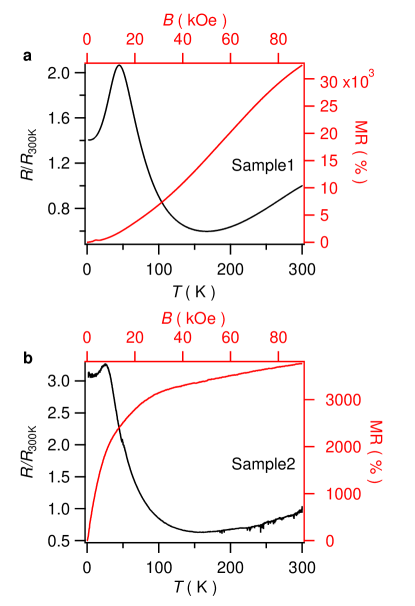
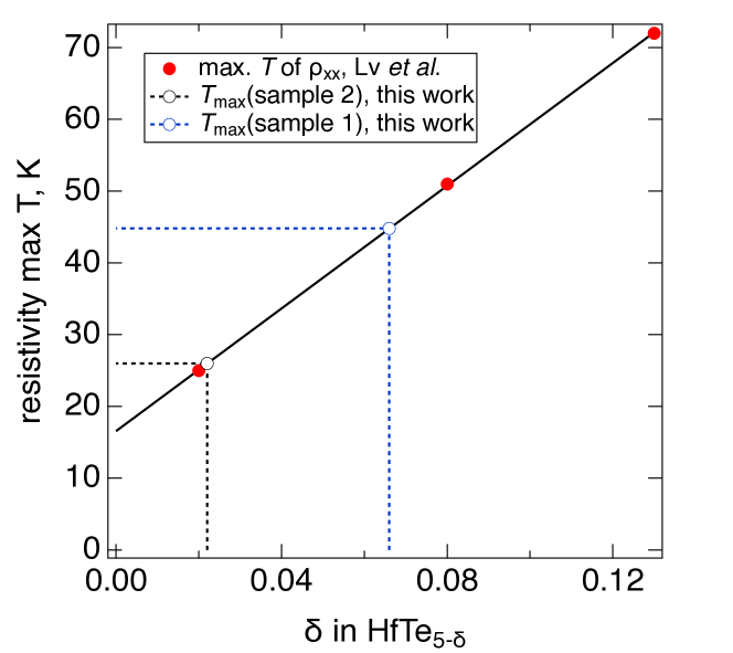
We grew single crystals of HfTe5 with different concentrations of Te-vacancies [31] by adjusting annealing temperatures after the growth (details can be found in Methods). Electrical transport measurements were performed to characterize those samples. As shown in Fig. 1, the temperature of maximum relative resistance, , for sample 1 is higher () than that of sample 2 (). Additionally, magnetoresistance (MR=100)) behaviors are very different: first, sample 1 has almost one order higher MR value at 90 kOe compared to the MR of sample 2. Second, MR saturates around 20 kOe for sample 2, while it does not saturate until 90 kOe for sample 1. These electrical transport behavior reproduce the results of reference [31] quite well. By comparing our transport results to [31], it is clear that sample 2 has fewer Te vacancies than sample 1, likely a result of its lower post-annealing temperature. The observed linear relationship between and [31] in HfTe5-δ[31] was used to estimate (0.066, 0.022) for samples (1,2), respectively (see Fig. S3).
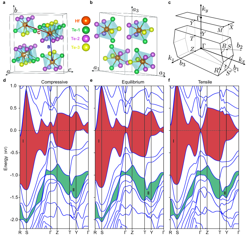
We first consider the influence of Te vacancies on our structural and electronic properties via DFT calculations for HfTe5 in the structure. The conventional unit cell consists of four Hf-Te zig-zag chains along the unit cell direction, as indicated in Fig. 2(a). Within each chain, the atoms are strongly bonded, while the chain-chain bonding is of a weak van der Waals type. There are three unique Te sites (Te-1, Te-2, Te-3). Each Hf atom is bonded to two singly-coordinated Te-1 atoms perpendicular to the chains, while Te-2 and Te-3 are doubly coordinated to Hf and participate in the zig-zag chain structures. We define three relevant Hf-Hf distances: (intra-chain separation), and (inter-chain separations roughly along conventional unit cell axes , respectively, see Fig. 2(a)).
The results of our full structural optimizations with vacancies are summarized in Fig.S7. We find that Te-2 is the lowest energy defect site; in comparison, Te-1 and Te-3 have energies 2.29 meV and 8.54 meV higher per atom, respectively. Te-1 vacancies reduce the intra-chain separation and inter-chain separation by about 3%, while the Te-2 vacancy has minimal effect on those two distances. Both vacancies lead to a slight increase in the Hf-Hf inter-chain separation. Since both vacancies are overall quite close in energy, and much more favorable than the Te-3 vacancy, we can conclude that defects induce a compression along , accompanied by a slight increase in the Hf-Hf inter-chain separation and another reduction in the Hf-Hf inter-chain separation.
| 2% Compressive | Equilibrium | 2% Tensile | ||||
|---|---|---|---|---|---|---|
| Gap | Class | Class | Class | |||
| I | (1;110) | Strong | (1;110) | Strong | (0;110) | Weak |
| II | (0;110) | Weak | (0;110) | Weak | (0;110) | Weak |
Considering the association of Te vacancies with compaction of the Hf-Hf inter-chain distance , we hypothesize that compressive uniaxial strain along the crystallographic direction is a proxy for Te vacancies, or conversely, tensile uniaxial stress along may suppress the effects of Te vacancies. To simulate strain along the -axis in our calculations (i.e., along the Hf-Hf chain direction), we artificially fixed the lattice parameter, and found the corresponding optimal lattice parameters for and for each value of strain considered (2% uniaxial compressive and tensile strain). For all cases, full internal coordinate optimizations were performed.
The bulk primitive electronic structures at the three different levels of strain are shown in Fig. 2(d-f). We find two topological gaps of interest, labeled (I) and (II), whose topological invariants are summarized in Table 1. Gap (I) is a strong gap in the -2% (compressive) and 0% (equilibrium) strain cases, and a weak gap in the case of +2% (tensile) strain. Gap (II) is a weak gap at all strain levels. We conclude that in the absence of defects, HfTe5 undergoes a STI WTI topological phase transition between 0 and 2% tensile strain. Note that the 2% compressive strain case cannot be rigorously labeled a strong topological insulator since the bulk system is metallic, as shown in Fig. 2(d). However, the band structure in Fig. 2(d) can be adiabatically deformed so that no bands cross the Fermi level. Thus, HfTe5, under 2% compressive strain is equivalent to a strong topological insulator from the perspective of band topology. We expect that HfTe5 remains an insulator when smaller compressive strains are applied.
A topological surface state at the point at the Fermi energy is shown in Fig. 3 (b), (d), and (e). This state lies in gap (I), which is a strong topological gap at equilibrium and with compressive strain, so we expect an odd number of topological surface states [32, 33] (namely, one topological state at equilibrium in this system). With tensile strain, gap (I) becomes weak and the topological surface state at is gapped out (Fig. 3 (c) and (f)). No topological surface states are present on the surface in gap (I) with tensile strain, however. If we identify the surface with the reciprocal lattice vector, then we have , where . Thus, in the weak TI state, the surface cannot host any topological surface states [32, 33] in gap (I).
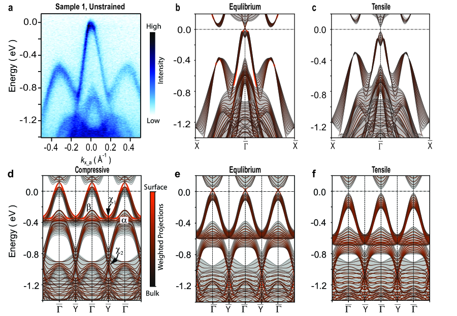
To experimentally verify the DFT predictions, we performed strain-dependent ARPES experiments on samples with different Te vacancy densities. Fig. 3 (a) shows a band structure cut along the , which corresponds to the direction. The topological surface state at the Fermi energy is not clearly resolved from the bulk states, similar to previous ARPES studies for ZrTe5 and HfTe5 [12, 16, 18], but overall band structures are amazingly well matched with the DFT calculations. More detailed measurements were performed along the direction. Figs. 4(b-f) are band structure cuts along the high symmetry line , which corresponds to the -axis or direction perpendicular to the Hf chains. Each band structure map corresponds to a different defect density and strain, as summarized schematically in Fig. 4(a) for sample 1 (more defects, blue symbols) and sample 2 (fewer defects, red symbols).
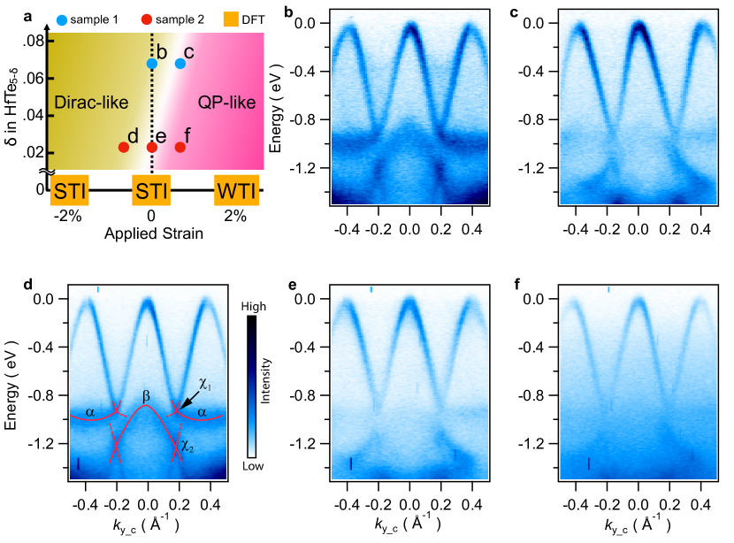
We first discuss the effect of defect density for unstrained samples (Figs. 4(b,e)). Although there is little observed difference between the band structures near the Fermi energy, clear differences can be observed near binding energy 1 eV. Interestingly, two Dirac-like band crossings labelled (), appear at =0.2 and 0.95eV and 1.2 eV in Fig. 4(b). These linear crossings (labelled in Fig. 4(d) where they also appear) are connected, respectively, by relatively flat bands and a hole band . It should be noted that, while in a repeated zone scheme and bands are present in every BZ, matrix element effects modulate the strength of these bands such that is suppressed in the central zone and is suppressed in the second (outer) BZs.
A primary finding of this work is that the features , , and in Fig. 4(b) vanish when defect density is reduced, Fig. 4(e). These results demonstrate that these features are strongly enhanced by defects in unstrained samples, a counter-intuitive result since one usually expects defects to weaken, not enhance, spectral weight. Close inspection of Fig. 4(e) reveals some weak remnant intensity of the , bands, but the crossings are replaced by some states around -1.3 eV with clearly different dispersion.
Now we discuss the application of uniaxial stress along the direction, i.e., in the Hf-Hf chain direction. The resulting strains are estimated to be in the range 0.7% based on strain gauge measurements with the same experimental configuration. (see Fig. S2 and Fig. S4(a).) For a high defect density combined with tensile strain (sample 1, Fig. 4(c)), the , , and bands are greatly diminished, similar to unstrained sample 2 (Fig. 4(e)). In fact the spectral functions in Figs. 4(c,e) are practically indistinguishable, the main difference being that the spectra from the sample with more defects (1) has a higher diffuse background. On the other hand, applying compressive strain to sample 2 results in the re-appearance of the , , and bands (Fig. 4(d)), with spectral function very similar to Fig. 4(b). On the other hand, in the case of tensile strain, the surface bands are completely extinguished and there is a notable rise in the diffuse background (Fig. 4(f)), which increases systematically towards higher binding energies. The changes in Figs. 4(d-f) are fully reversible (see Fig. S4). These changes indicate that with compressive strain, the quasiparticle scattering rate dramatically diminishes, while with tensile strain, there is a large enhancement of the quasiparticle scattering rate, suggestive of enhanced Fermi liquid-type excitations.
From these observations we can conclude the following: (1) The similarity of Figs. 4(b,d) and of Figs. 4(c,e) confirms our hypothesis that defects play a similar role as compressive strain along the chain with respect to promoting the appearance of the states , , and ; (2) these bands appear in HfTe5-δ as a consequence of the lattice changes induced by defects and are not derived from local electronic states directly associated with the defects; (3) defects and tensile strain independently increase the scattering rate, while compression reduces it; (4) up to the maximum applied strain we do not increase the number of defects; this follows from the reversibility of the changes in Figs. 4(d-f) and S4.
The phase diagram in Fig. 4(a) summarizes the observed phases. The upper left region (more defects and/or compressive strain) has a Dirac-like spectrum characterized by the appearance of the and bands connecting linear crossings around eV. The lower right region (fewer defects and/or tensile strain) is characterized by the absence of these states. Furthermore, there is a strong correlation between tensile strain applied along the -axis and the quasiparticle scattering rate. The latter represents a transition towards a liquid-like quasiparticle (QP) phase, characterized by spectral weight transfer from the bands to a strong diffuse background that increases systematically with binding energy.
To understand these features around eV, we next compare our ARPES results to the DFT results. We note that the strain considered in the DFT calculations is about three times the strain on the sample in the experimental measurements, thus the changes are more pronounced between the compressive strain, equilibrium, and tensile strain band structures. However, the equilibrium DFT calculation results (Fig. 4(h)) reproduce the essential features of unstrained sample 1 (Fig. 4(b)) and compressed sample 2 (Fig. 4(d)), namely the shapes and relative locations of bands and crossings . Since the calculation does not include photoemission matrix element effects, the bands appear equally in all BZs.
From these surface electronic structure calculations, we next interrogate the surface projected bands for the presence of topologically protected states. Although both are suggestive of Dirac crossings, neither of them are predicted by DFT to be a topological surface state. Since gap (II) is a weak gap, we expect an even number of topological surface states [32, 33]. However, since we have , similar to gap (I), no topologically non-trivial surface states can be expected on the surface of HfTe5 in gap (I) for the same reason previously discussed.
Considering the and crossings bands are not directly related to the TI surface states, the enhancement of the spectral weight of the bands with more defects is counter-intuitive. Thus, it leads us to connect with the topological phase transition near the Fermi energy. For TI surface states at/near the Fermi energy, the interplay between topology and disorder effects has been well studied [33]: surface states of a strong/weak TI are robust/vulnerable against charge disorders and thus the surface is expected to be conductive/insulating. In contrast, at energy far away from the Fermi energy (e.g., in the gap between two valence bands), impurities also have some nontrivial impact on surface states, through a different mechanism: broadening of line width due to disorder potentials. In contrast to a homogeneous electric potential, which shifts the energy of all bands by a constant amount, random potentials created by charge impurities provide random shifts, which results in a broadening of the line width. For the surface of a strong TI, the conducting topological surface state screens the Coulomb potential from charge impurities, reducing the disorder potential and thus leading to a sharper spectrum. This effect applies equally to surface states both near and away from the Fermi energy. In contrast, for weak TIs, such screening effects are absent, and thus the spectrum becomes more diffusive. As a result, if a material undergoes a topological phase transition from a strong TI to a weak TI, this effect implies that surface states away from the Fermi energy shall suffer more from impurity potential in the weak TI phase. This surface screening effect will logically affect the surface states most strongly. This is largely consistent with what was observed in the ARPES measurement, where the surface states ( and crossings ) become diffusive in the weak TI phase, while bulk states at the same energy range remain largely unchanged.
What remains to be explained is the reversible correlation between the topological class and the notable changes to the diffuse scattering background, which reflect coherence-limiting scattering processes that occur during photoemission. While a quantitative explanation for this effect is beyond the scope of this study, we can suggest three qualitative explanations: (1) the screening near the surface is reduced by the absence of metallic topological states in the WTI phase, thus the scattering of bulk states near the surface (that dominate the ARPES signal) is enhanced in the WTI phase. This leads to the QP-like increase in scattering rates towards higher binding energy in the WTI phase; (2) tensile strain reduces the electron density along the Hf chains, thus similarly reducing the bulk screening and enhancing the QP scattering rate in the bulk; (3) defects such as dislocations are created upon tensile strain and reversibly destroyed when strain is relieved or compressive strain applied. (We find this explanation unlikely given that we are below the plastic deformation regime, but we mention the possibility for completeness.)
Since we can assume that the diffuse background is dominated by the QP scattering of bulk state[34], the key to distinguishing effects (1) and (2) is the behavior of the momentum broadening of the bulk states with strain. For weakly-correlated systems, the bulk states’ momentum width at binding energy from ARPES is directly proportional to the imaginary part of the self-energy function, which reflects the electron lifetime to all scattering from phonons, defects, or other electrons. For (1), we would expect an abrupt general increase in as we transition from STI to WTI, and for (2) we would expect a continual decrease in scattering as we go from tensile to compressive strain, regardless of topological phase transition.
While our analysis of the bulk states’ momentum spread has not revealed a clear evolution with strain (see Fig. S8), favoring explanation (1), it remains possible that the changes in are below our experimental resolution, or that the observed is dominated by inhomogeneous broadening effects.
Nevertheless, our results strongly suggest that the self-energy of both surface and bulk electronic (trivial) states are strongly impacted by the presence of topological surface states, an effect not seen before in ARPES to our knowledge. Our results further demonstrate strain control of topological states as a new method to tune or optimize the coherence of electronic excitations, even overcoming scattering by unavoidably present defects, to improve the performance of quantum materials in new device schemes.
I Data availability
Data underlying these results are available from the authors, see Additional Information below.
II References and notes
References
- Chen et al. [2010] Y. Chen, J.-H. Chu, J. Analytis, Z. Liu, K. Igarashi, H.-H. Kuo, X. Qi, S.-K. Mo, R. Moore, D. Lu, et al., Massive Dirac fermion on the surface of a magnetically doped topological insulator, Science 329, 659 (2010).
- Zhang et al. [2019] D. Zhang, M. Shi, T. Zhu, D. Xing, H. Zhang, and J. Wang, Topological Axion States in the Magnetic Insulator MnBi2Te4 with the Quantized Magnetoelectric Effect, Phys. Rev. Lett. 122, 206401 (2019).
- Li et al. [2019] J. Li, Y. Li, S. Du, Z. Wang, B.-L. Gu, S.-C. Zhang, K. He, W. Duan, and Y. Xu, Intrinsic magnetic topological insulators in van der Waals layered MnBi2Te4-family materials, Science Advances 5, eaaw5685 (2019).
- Otrokov et al. [2019] M. M. Otrokov, I. I. Klimovskikh, H. Bentmann, D. Estyunin, A. Zeugner, Z. S. Aliev, S. Gaß, A. Wolter, A. Koroleva, A. M. Shikin, et al., Prediction and observation of an antiferromagnetic topological insulator, Nature 576, 416 (2019).
- Jo et al. [2020] N. H. Jo, L.-L. Wang, R.-J. Slager, J. Yan, Y. Wu, K. Lee, B. Schrunk, A. Vishwanath, and A. Kaminski, Intrinsic axion insulating behavior in antiferromagnetic MnBi6Te10, Phys. Rev. B 102, 045130 (2020).
- Frey et al. [2020] N. C. Frey, M. K. Horton, J. M. Munro, S. M. Griffin, K. A. Persson, and V. B. Shenoy, High-throughput search for magnetic and topological order in transition metal oxides, Science advances 6, eabd1076 (2020).
- Li et al. [2016a] Q. Li, D. E. Kharzeev, C. Zhang, Y. Huang, I. Pletikosić, A. Fedorov, R. Zhong, J. Schneeloch, G. Gu, and T. Valla, Chiral magnetic effect in ZrTe5, Nature Physics 12, 550 (2016a).
- Chen et al. [2015a] R. Y. Chen, Z. G. Chen, X.-Y. Song, J. A. Schneeloch, G. D. Gu, F. Wang, and N. L. Wang, Magnetoinfrared Spectroscopy of Landau Levels and Zeeman Splitting of Three-Dimensional Massless Dirac Fermions in ZrTe5, Phys. Rev. Lett. 115, 176404 (2015a).
- Chen et al. [2015b] R. Y. Chen, S. J. Zhang, J. A. Schneeloch, C. Zhang, Q. Li, G. D. Gu, and N. L. Wang, Optical spectroscopy study of the three-dimensional Dirac semimetal ZrTe5, Phys. Rev. B 92, 075107 (2015b).
- Zheng et al. [2016] G. Zheng, J. Lu, X. Zhu, W. Ning, Y. Han, H. Zhang, J. Zhang, C. Xi, J. Yang, H. Du, K. Yang, Y. Zhang, and M. Tian, Transport evidence for the three-dimensional Dirac semimetal phase in ZrTe5, Phys. Rev. B 93, 115414 (2016).
- Shen et al. [2017] L. Shen, M. Wang, S. Sun, J. Jiang, X. Xu, T. Zhang, Q. Zhang, Y. Lv, S. Yao, Y. Chen, M. Lu, Y. Chen, C. Felser, B. Yan, Z. Liu, L. Yang, and Y. Chen, Spectroscopic evidence for the gapless electronic structure in bulk ZrTe5, Journal of Electron Spectroscopy and Related Phenomena 219, 45 (2017).
- Wu et al. [2016] R. Wu, J.-Z. Ma, S.-M. Nie, L.-X. Zhao, X. Huang, J.-X. Yin, B.-B. Fu, P. Richard, G.-F. Chen, Z. Fang, X. Dai, H.-M. Weng, T. Qian, H. Ding, and S. H. Pan, Evidence for Topological Edge States in a Large Energy Gap near the Step Edges on the Surface of ZrTe5, Phys. Rev. X 6, 021017 (2016).
- Li et al. [2016b] X.-B. Li, W.-K. Huang, Y.-Y. Lv, K.-W. Zhang, C.-L. Yang, B.-B. Zhang, Y. B. Chen, S.-H. Yao, J. Zhou, M.-H. Lu, L. Sheng, S.-C. Li, J.-F. Jia, Q.-K. Xue, Y.-F. Chen, and D.-Y. Xing, Experimental Observation of Topological Edge States at the Surface Step Edge of the Topological Insulator ZrTe5, Phys. Rev. Lett. 116, 176803 (2016b).
- Manzoni et al. [2015a] G. Manzoni, A. Sterzi, A. Crepaldi, M. Diego, F. Cilento, M. Zacchigna, P. Bugnon, H. Berger, A. Magrez, M. Grioni, and F. Parmigiani, Ultrafast Optical Control of the Electronic Properties of ZrTe5, Phys. Rev. Lett. 115, 207402 (2015a).
- Zhang et al. [2017a] Y. Zhang, C. Wang, L. Yu, G. Liu, A. Liang, J. Huang, S. Nie, X. Sun, Y. Zhang, B. Shen, et al., Electronic evidence of temperature-induced Lifshitz transition and topological nature in ZrTe5, Nature communications 8, 1 (2017a).
- Moreschini et al. [2016] L. Moreschini, J. C. Johannsen, H. Berger, J. Denlinger, C. Jozwiak, E. Rotenberg, K. S. Kim, A. Bostwick, and M. Grioni, Nature and topology of the low-energy states in ZrTe5, Phys. Rev. B 94, 081101 (2016).
- Manzoni et al. [2016] G. Manzoni, L. Gragnaniello, G. Autès, T. Kuhn, A. Sterzi, F. Cilento, M. Zacchigna, V. Enenkel, I. Vobornik, L. Barba, F. Bisti, P. Bugnon, A. Magrez, V. N. Strocov, H. Berger, O. V. Yazyev, M. Fonin, F. Parmigiani, and A. Crepaldi, Evidence for a Strong Topological Insulator Phase in ZrTe5, Phys. Rev. Lett. 117, 237601 (2016).
- Liu et al. [2018] S. Liu, M. Wang, C. Chen, X. Xu, J. Jiang, L. Yang, H. Yang, Y. Lv, J. Zhou, Y. Chen, et al., Experimental observation of conductive edge states in weak topological insulator candidate HfTe5, APL Materials 6, 121111 (2018).
- Nair et al. [2018] N. L. Nair, P. T. Dumitrescu, S. Channa, S. M. Griffin, J. B. Neaton, A. C. Potter, and J. G. Analytis, Thermodynamic signature of dirac electrons across a possible topological transition in , Phys. Rev. B 97, 041111 (2018).
- McIlroy et al. [2004] D. N. McIlroy, S. Moore, D. Zhang, J. Wharton, B. Kempton, R. Littleton, M. Wilson, T. M. Tritt, and C. G. Olson, Observation of a semimetal-semiconductor phase transition in the intermetallic ZrTe5, Journal of Physics: Condensed Matter 16, L359 (2004).
- Manzoni et al. [2015b] G. Manzoni, A. Sterzi, A. Crepaldi, M. Diego, F. Cilento, M. Zacchigna, P. Bugnon, H. Berger, A. Magrez, M. Grioni, and F. Parmigiani, Ultrafast Optical Control of the Electronic Properties of ZrTe5, Phys. Rev. Lett. 115, 207402 (2015b).
- Zhang et al. [2017b] Y. Zhang, C. Wang, L. Yu, G. Liu, A. Liang, J. Huang, S. Nie, X. Sun, Y. Zhang, B. Shen, et al., Electronic evidence of temperature-induced Lifshitz transition and topological nature in ZrTe5, Nature communications 8, 1 (2017b).
- Tang et al. [2019] F. Tang, Y. Ren, P. Wang, R. Zhong, J. Schneeloch, S. A. Yang, K. Yang, P. A. Lee, G. Gu, Z. Qiao, et al., Three-dimensional quantum Hall effect and metal–insulator transition in ZrTe5, Nature 569, 537 (2019).
- Liu et al. [2016] Y. Liu, X. Yuan, C. Zhang, Z. Jin, A. Narayan, C. Luo, Z. Chen, L. Yang, J. Zou, X. Wu, et al., Zeeman splitting and dynamical mass generation in Dirac semimetal ZrTe5, Nature communications 7, 1 (2016).
- Galeski et al. [2021] S. Galeski, T. Ehmcke, R. Wawrzyńczak, P. M. Lozano, K. Cho, A. Sharma, S. Das, F. Küster, P. Sessi, M. Brando, et al., Origin of the quasi-quantized Hall effect in ZrTe5, Nature communications 12, 1 (2021).
- Zhou et al. [2016] Y. Zhou, J. Wu, W. Ning, N. Li, Y. Du, X. Chen, R. Zhang, Z. Chi, X. Wang, X. Zhu, P. Lu, C. Ji, X. Wan, Z. Yang, J. Sun, W. Yang, M. Tian, Y. Zhang, and H. kwang Mao, Pressure-induced superconductivity in a three-dimensional topological material ZrTe5, Proceedings of the National Academy of Sciences 113, 2904 (2016).
- Mutch et al. [2019] J. Mutch, W.-C. Chen, P. Went, T. Qian, I. Z. Wilson, A. Andreev, C.-C. Chen, and J.-H. Chu, Evidence for a strain-tuned topological phase transition in ZrTe5, Science advances 5, eaav9771 (2019).
- Zhang et al. [2021] P. Zhang, R. Noguchi, K. Kuroda, C. Lin, K. Kawaguchi, K. Yaji, A. Harasawa, M. Lippmaa, S. Nie, H. Weng, et al., Observation and control of the weak topological insulator state in ZrTe5, Nature communications 12, 1 (2021).
- Hochberg et al. [2018] Y. Hochberg, Y. Kahn, M. Lisanti, K. M. Zurek, A. G. Grushin, R. Ilan, S. M. Griffin, Z.-F. Liu, S. F. Weber, and J. B. Neaton, Detection of sub-mev dark matter with three-dimensional dirac materials, Physical Review D 97, 015004 (2018).
- Monserrat and Narayan [2019] B. Monserrat and A. Narayan, Unraveling the topology of by changing temperature, Phys. Rev. Res. 1, 033181 (2019).
- Lv et al. [2018] Y.-Y. Lv, X. Li, L. Cao, D. Lin, S.-H. Yao, S.-S. Chen, S.-T. Dong, J. Zhou, Y. B. Chen, and Y.-F. Chen, Tunable Resistance or Magnetoresistance Cusp and Extremely Large Magnetoresistance in Defect-Engineered HfTe5-δ Single Crystals, Phys. Rev. Applied 9, 054049 (2018).
- Fu and Kane [2007] L. Fu and C. L. Kane, Topological insulators with inversion symmetry, Physical Review B 76 (2007).
- Fu et al. [2007] L. Fu, C. L. Kane, and E. J. Mele, Topological insulators in three dimensions, Physical Review Letters 98 (2007).
- Cai et al. [2018] S. Cai, J. Guo, V. A. Sidorov, Y. Zhou, H. Wang, G. Lin, X. Li, Y. Li, K. Yang, A. Li, Q. Wu, J. Hu, S. K. Kushwaha, R. J. Cava, and L. Sun, Independence of topological surface state and bulk conductance in three-dimensional topological insulators, npj Quantum Materials 3, 62 (2018).
- Jo et al. [2019] N. H. Jo, L.-L. Wang, P. P. Orth, S. L. Bud’ko, and P. C. Canfield, Magnetoelastoresistance in WTe2: Exploring electronic structure and extremely large magnetoresistance under strain, Proceedings of the National Academy of Sciences 116, 25524 (2019).
- Kresse and Hafner [1993] G. Kresse and J. Hafner, Ab initio molecular dynamics for liquid metals, Phys. Rev. B 47, 558 (1993).
- Kresse and Hafner [1994] G. Kresse and J. Hafner, Ab initio molecular-dynamics simulation of the liquid-metal–amorphous-semiconductor transition in germanium, Phys. Rev. B 49, 14251 (1994).
- Kresse and Furthmüller [1996] G. Kresse and J. Furthmüller, Efficiency of ab-initio total energy calculations for metals and semiconductors using a plane-wave basis set, Computational Materials Science 6, 15 (1996).
- Kresse and Furthmüller [1996] G. Kresse and J. Furthmüller, Efficient iterative schemes for ab initio total-energy calculations using a plane-wave basis set, Phys. Rev. B 54, 11169 (1996).
- Kresse and Joubert [1999] G. Kresse and D. Joubert, From ultrasoft pseudopotentials to the projector augmented-wave method, Phys. Rev. B 59, 1758 (1999).
- Fjellvåg and Kjekshus [1986] H. Fjellvåg and A. Kjekshus, Structural properties of ZrTe5 and HfTe5 as seen by powder diffraction, Solid State Communications 60, 91 (1986).
- Pizzi et al. [2020] G. Pizzi, V. Vitale, R. Arita, S. Blügel, F. Freimuth, G. Géranton, M. Gibertini, D. Gresch, C. Johnson, T. Koretsune, J. Ibañez-Azpiroz, H. Lee, J. Lihm, D. Marchand, A. Marrazzo, Y. Mokrousov, J. Mustafa, Y. Nohara, Y. Nomura, L. Paulatto, S. Poncé, T. Ponweiser, J. Qiao, F. Thöle, S. Tsirkin, M. Wierzbowska, N. Marzari, D. Vanderbilt, I. Souza, A. Mostofi, and J. Yates, Wannier90 as a community code: new features and applications., J Phys Condens Matter 32, 165902 (2020).
- Wu et al. [2018] Q. Wu, S. Zhang, H.-F. Song, M. Troyer, and A. A. Soluyanov, Wanniertools : An open-source software package for novel topological materials, Computer Physics Communications 224, 405 (2018).
- He et al. [2019] Y. He, Y. Jiang, T. Zhang, H. Huang, C. Fang, and Z. Jin, Symtopo:an automatic tool for calculating topological properties of nonmagnetic crystalline materials, Chinese Physics B 28, 087102 (2019).
- Iraola et al. [2022] M. Iraola, J. L. Mañes, B. Bradlyn, M. K. Horton, T. Neupert, M. G. Vergniory, and S. S. Tsirkin, Irrep: Symmetry eigenvalues and irreducible representations of ab initio band structures, Computer Physics Communications 272, 108226 (2022).
- Elcoro et al. [2017] L. Elcoro, B. Bradlyn, Z. Wang, M. G. Vergniory, J. Cano, C. Felser, B. A. Bernevig, D. Orobengoa, G. de la Flor, and M. I. Aroyo, Double crystallographic groups and their representations on the Bilbao Crystallographic Server, Journal of Applied Crystallography 50, 1457 (2017).
- Vergniory et al. [2022] M. G. Vergniory, B. J. Wieder, L. Elcoro, S. S. P. Parkin, C. Felser, B. A. Bernevig, and N. Regnault, All topological bands of all nonmagnetic stoichiometric materials, Science 376, eabg9094 (2022), https://www.science.org/doi/pdf/10.1126/science.abg9094 .
- Hicks et al. [2014] C. W. Hicks, M. E. Barber, S. D. Edkins, D. O. Brodsky, and A. P. Mackenzie, Piezoelectric-based apparatus for strain tuning, Review of Scientific Instruments 85, 065003 (2014).
III Acknowledgement
This material is based upon work at the QSA, supported by the U.S. Department of Energy, Office of Science, National Quantum Information Science Research Centers. This research used resources of the Advanced Light Source, which is a DOE Office of Science User Facility under contract no. DE-AC02-05CH11231. This work was also supported by the DOE’s Quantum Information Science Enabled Discovery (QuantISED) for High Energy Physics (KA2401032). Computational resources were provided by the National Energy Research Scientific Computing Center and the Molecular Foundry, DOE Office of Science User Facilities supported under Contract No. DEAC02-05-CH11231. The work performed at the Molecular Foundry was supported by the Office of Science, Office of Basic Energy Sciences, of the U.S. Department of Energy under the same contract. O.A.A. acknowledges helpful discussions with I. Na and E. Banyas.
IV Author contributions
N.H.J. and E.R. conceived of the presented idea. A.S. and T.K. synthesized the single crystal and performed X-ray diffraction and electrical transport measurements. N.H.J, C.J., A.B., S.H.R, and E.R. conducted the ARPES experiment. O.A.A. and S.M.G. performed the DFT calculations and topological characterization. O.A.A., K.S., and S.M.G. carried out theoretical analysis. N.H.J., O.A.A., K.S., T.K., S.M.G., and E.R. wrote the manuscript in consultation with Z.S., C.J. A.B., and S.H.R.
V Competing financial interests
The authors declare no competing financial interests.
VI Additional information
Correspondence and requests for materials should be addressed to N. H. Jo, S. M. Griffin, and E. Rotenberg.
VII Methods
Crystal growth. Single crystals of HfTe5 were grown using tellurium flux. Hafnium powder (Alfa Aesar, 99.6 metals basis excluding Zr, Zr nominal 2-3.5 ) and a tellurium lump (Alfa Aesar, 99.999), in the atomic ratio of Hf:Te = 1:99, were sealed in a silica tube under vacuum. The growth was heated up to 650 oC in 3 hours, dwell for 10 hours, and then slowly cooled to 460∘C over 78 hours before decanting. Low temperature annealing was conducted at 380∘C and 250∘C for 5 days in a sealed silica tube for sample 1 and sample 2, respectively. The samples crystallize in space group number 63 (). The lattice parameters for the single crystals are 3.97 Å-1, 14.5 Å-1, and 13.7 Å-1.
Electrical transport measurements. Resistance measurements down to 1.8 K were conducted using a Quantum Design physical property measurement system (PPMS) Dynacool using the resistivity option. Pt wires were attached to the samples using DuPont silver paint (4929N) in a standard 4-probe configuration. Magnetic field (0-90 kOe) was applied perpendicular to -axis.
ARPES measurements. ARPES experiments were conducted at the Beamline 7.0.2 (MAESTRO) at the Advanced Light Source. The data were acquired using the micro-ARPES endstation, which consists of an Omicron Scienta R4000 electron analyzer. Samples were cleaved by carefully knocking off an alumina post that is attached on top of each sample with silver epoxy. Data were collected with photon energies of 101 eV, which accesses near the plane of the Brillouin Zone (BZ). The beam size was 15m 15m. ARPES measurements were performed at 200 K under ultra-high vacuum (UHV) better than 4 10-11 torr.
As shown in Fig. 2(a), HfTe5 has a weak van der Waals bonding along the crystallographic direction; thus, the cleaved surface was -plane. Note that, by ARPES convention, is normal to the cleaved surface. Therefore, we define , , and as directed along the crystallographic , , and , respectively.
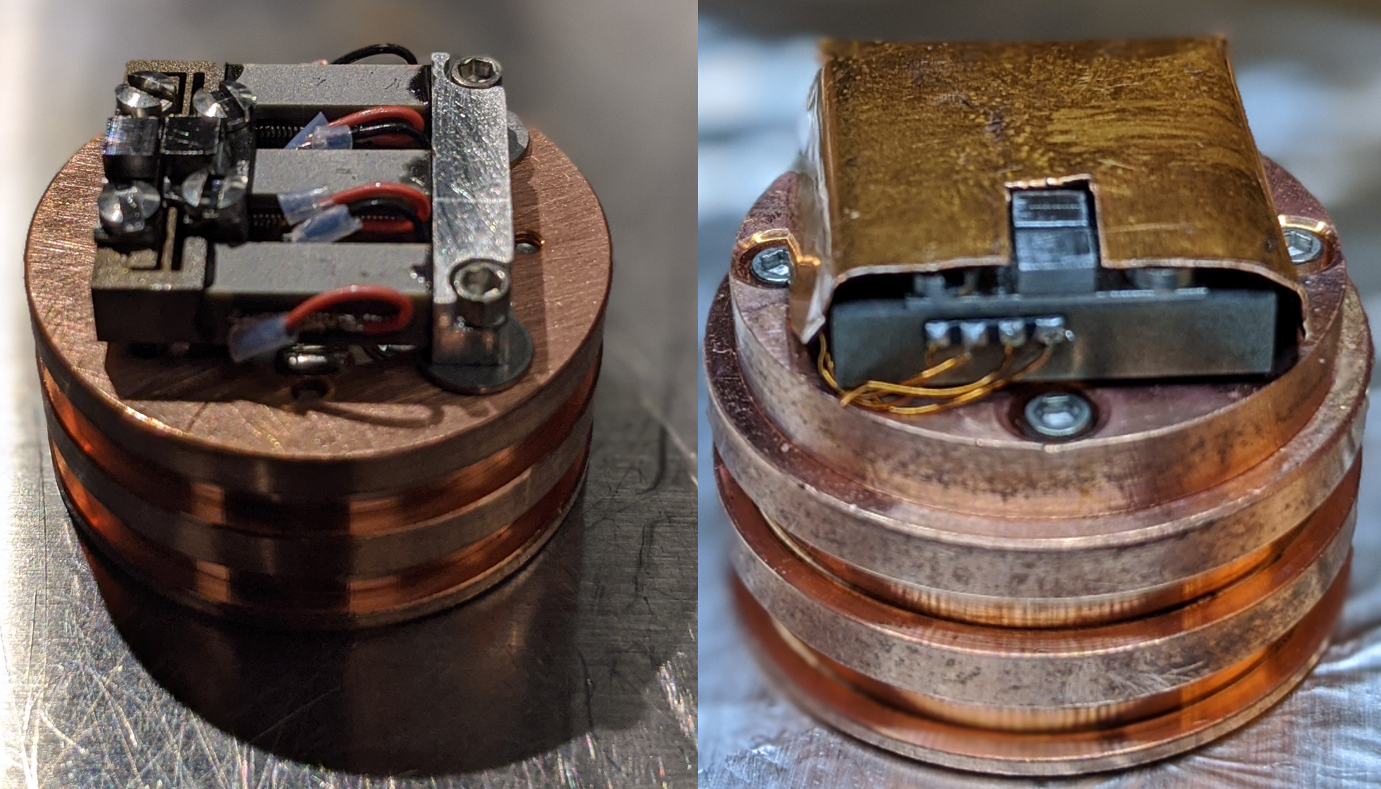
Uniaxial stress. ARPES measurements under uniaxial stress were carried out using a custom-built uniaxial stress cell, as shown in Fig. S1. Samples were mounted with Stycast epoxy (2850FT). After curing the epoxy, we put silver paste (Dupont, 4929N) on top to ground the sample. The uniaxial stress was applied on samples along the crystallographic direction. In this experimental configuration, three strain tensor components were nonzero in Voigt notation[35]. We measured the strain tensor component with a strain gauge (Fig. S2), and the maximum tensile/compress strain was 0.7%. Detailed information about the cell can be found in SI. In order to keep the same beam spot on the sample, we used a microscope in the -ARPES chamber. In addition, we performed scan on the sample with 10m step size and slit-deflector scan each and every time we change the strain on the sample. Note that we obtained the unstrained data after cooling down the cell but before applying any voltages on the piezo actuators. Even though no voltages are applied, the thermal contraction of the cell, which is most likely different from the thermal contraction of the sample, does slightly exist.
DFT calculations. Our DFT calculations were performed using the Vienna Ab initio Simulation Package (vasp) [36, 37, 38, 39] using the projector augmented wave (PAW) method [40]. All calculations in the main text use the primitive cell, except those for Fig. S7 which used a supercell of 96 atoms. Hf(5p, 6s, 5d) and Te(5s, 5p); electrons were treated as valence. We expanded the wavefunction plane waves to an energy cutoff of 600 eV, and used -centered k-point grids of for the conventional cell, for the primitive cell for structural optimizations, and for the supercell defect structural optimizations. An grid was used with the conventional cell for accurate electronic structure calculations and to generate the Wannier-based tight-binding model. We did not include spin-orbit coupling in our structural optimizations as it was found to have minimal influence on the calculated lattice parameters, however, we included spin-orbit coupling self-consistently in the electronic structure calculations where specified. The electronic convergence criterion is set to eV and the force convergence criterion is set to 0.005 eV / Å.
Prior DFT calculations on ZrTe5 and HfTe5 highlighted the importance of accurate calculations of the structural parameters, particularly owing to the extreme sensitivity of details of the electronic and topological properties on the volume and structure [29]. Therefore, we carefully chose our exchange-correlation functional by benchmarking against reported low-temperature X-ray diffraction measurements, finding PBEsol to give good agreement with the experiment. We calculated the lattice parameters to be a = 3.953 Å, b = 14.564 Å, and c = 13.622 Å using PBEsol, compared to the measured values of 3.964 Å, b = 14.443 Å, and c = 13.684 Åat 10 Km[41].
For the slab calculations, an 11-layer (132-atom) centrosymmetric slab with 15 Å of vacuum was utilized. We used a -centered k-grid, and spin-orbit coupling was included self-consistently. Line thickness and color scale in the slab band structures (Fig. 4 (b-f)) are given by Eq. (1) below
| (1) |
where is the Bloch function of band at k-point . is a localized atomic state with orbital quantum numbers (), centered at an atom with coordinates , where is the non-periodic direction of the slab. For a given band and -point in the band structure, we first sum over all quantum numbers () of atomic states , from all atoms with coordinates on a given plane . We finally sum over all the planes with various , with an exponential weighting factor that decays away from the surface of the slab at . The last sum is performed over the top half of the centrosymmetric slab, giving the weighted projections from one of the surfaces at . Here, we used Å-1.
Using our first-principles electronic structure, we constructed our Wannier function-based tight-binding models using the WANNIER90 package[42], including the Hf-d and Te-p orbitals as basis. Besides the explicit DFT slab calculations mentioned above, we further calculated the surface states by generating a semi-infinite slab configuration from our tight-binding model using the iterative Green’s function (IGF) method to generate surface Te-projected bands using the WannierTools [43] package. Finally, our topological invariants were calculated using symmetry indicators and DFT-calculated eigenvalues as implemented in the symtopo [44] package, irrep [45, 46] package and the Check Topological Mat. tool on the Bilbao Crystallographic Server [47].
Gaps (I) and (II) were checked across the entire irreducible Brillouin zone (IBZ) at all levels of strain to ensure the bands do not touch (i.e., the gap remains open) using a -grid of 363612. In all cases but one, the minimum gap size was on the order of 10 meV. However, the bands got closer than 10 meV in the case of gap (II) at equilibrium, so it was further checked with a dense cubic ‘patch’ centered around the k-point with the gap minimum. This calculation showed that the bands almost touch within 1 meV, which is beyond the resolution of DFT. Thus, gap (II) practically closes at this level of strain at the DFT level. However, since gap (II) is finite for both compressive and tensile strain, we expect any small deviation from the equilibrium structure calculated in DFT to result in gap (II) opening.
VIII Supplementary Information
S8.1 Uniaxial stress cell
The uniaxial stress cell we used for this experiment is based on three piezoelectric stacks, similar to Ref. [48]. As we have eight available electrical channels on our system, we used four to control the piezoelectric stacks and the rest of the four channels for strain gauge measurements. We attached a Cu thermal braiding near the sample in order to ground the sample and achieve better temperature control. In addition, we put a Cu shielding on top of the cell to shield the field from the piezoelectric stacks, as shown in Fig. S1 on the right side.
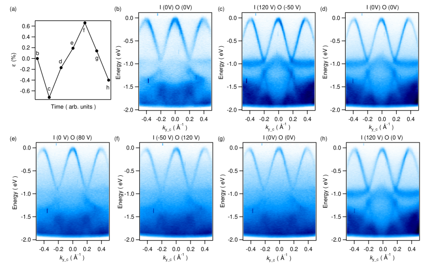
S8.2 Strain measurements
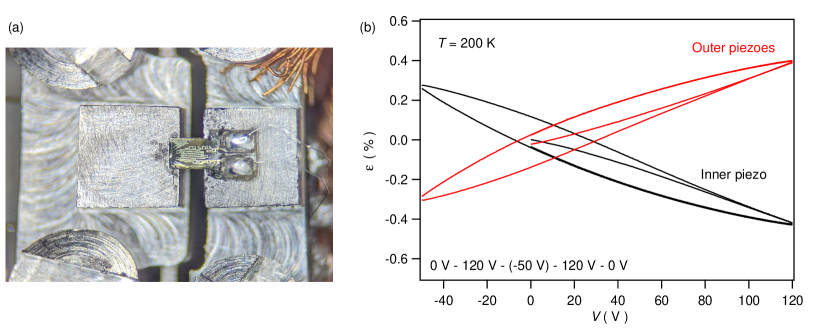
The strain was measured using a strain gauge (C5K-XX-S5198-350/39F, Micro-Measurements.) mounted with the Stycast epoxy (2850FT) underneath. We first drive the inner piezo actuator from 0 V to 120 V, followed by -50 V, back to 120 V, and ended up at 0 V. While applying voltage on the inner piezo actuator; the outer piezo actuators were connected in a short circuit. At the same time, we measured changes in the resistance of the strain gauge. With the given gauge factor of 1.84 from the manufacturer, the strain was calculated. The results are shown in Fig. S2 (b) in the black line. A clear hysteresis was detected with the maximum compressive strain of at 120 V and maximum tensile strain of at -50 V. We then put the inner piezo actuator in a short circuit and derive the outer piezo actuators with the same applied voltage sequence. The red line in Fig. S2 (b) shows a similar hysteresis loop but the opposite sign compared to the hysteresis loop from the inner piezo actuator. The maximum compressive strain of at -50 V and the maximum tensile strain of at 120 V were observed.
S8.3 Estimate of Defect Density
For the Te-poor compound HfTe5-δ, Lv et al. [31] have reported a linear relationship between the Te deficit with the temperature of the maximum longitudinal resistivity , which is plotted in Fig. S3 (red dots). Since this temperature is very similar to as defined in our main text, we have used their transport measurements to derive estimates of for our samples (1,2), which are = (.066, .022), respectively.
S8.4 Strain dependent band structure
Figure S4 presents band structure changes with full-cycle piezo actuator movements. (0 V - compress - tensile - compress) It demonstrates not only apparent changes in band structure with the applied uniaxial stress but also reproducible results.
S8.5 Comparison between ARPES and IGF calculations
Figures S5 (a)-(c) and (g)-(i) show constant energy contour plots of HfTe5 under compressive strain (sample 2). Corresponding IGF calculations are also plotted in Figs. S5 (d)-(f) and (j)-(l). The binding energies of each plot, Figs. S5 (a)-(l), are marked in Figs. S5 (m) and (n). Comparing ARPES and IGF calculations, we find that sample 2 with compressive strain (or unstrained sample 1) is very close to but not exactly the same as the equilibrium IGF calculation results. First of all, the chemical potential is shifted about 150 meV downward in ARPES data compared to the IGF calculations. More specifically, the Fermi surface from ARPES measurement is composed of dots which are the residual intensities from the top of the hole bands below (Fig. S5 (a)). On the other hand, crosses the hole bands in the IGF calculation. As a result, the astroid shape of the Fermi surface is observed in the IGF calculations (Fig. S5 (d)). The astroids become more clear at higher binding energies in both ARPES and IGF calculation results (Fig. S5 (b), (c), and (d)-(f)). ARPES results at the binding energies of 250 meV and 500 meV are very similar to the IGF calculation results at 100 meV and 300 meV, respectively. This means 150 meV - 200 meV band shifts in ARPES data. Secondly, the spacing between two surface bands, , and , gets larger with tensile strain in the IGF calculations. (See Fig. 4 (h) and (i)) In fact, the spacing between the surface bands in compressed sample 2 and unstrained sample 1 is slightly larger than that of the IGF calculation at equilibrium, which means the samples at those conditions are slightly stretched.
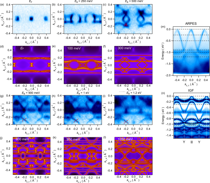
S8.6 Linear band crossings away from high symmetry points
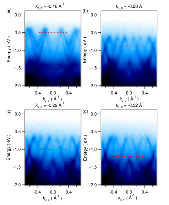
The astroids shown in Fig. S5 start to cross at = 500 meV. Crossing points are marked with red dashed lines in Figs. S5(c), and (g)-(i). With larger binding energy, the points move outwards in the direction. Interestingly, the crossing points of the steroids marked in Fig. S5 with red dashed lines correspond to linear crossing in the band structure as shown in Fig. S6.
S8.7 Effect of vacancies and strain on bond lengths
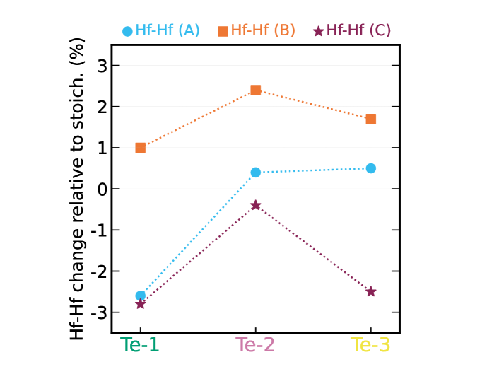
The structural changes are quantified by comparing the Hf-Hf nearest-neighbor distances in the A, B, and C directions as indicated on the crystal structure in Fig. 2(a) with the values for the stoichiometric case. For each calculation, one Te vacancy was included in a super cell comprising 16 formula units of HfTe5 resulting in a 1.25% defect density.
| Structure | A | B | C |
|---|---|---|---|
| 2% Compressive | 3.876 | 7.547 | 7.337 |
| Equilibrium | 3.953 | 7.545 | 7.327 |
| 2% Tensile | 4.034 | 7.554 | 7.311 |
| Te-1 Vacancy | 3.927 | 7.555 | 7.299 |
| Te-2 Vacancy | 3.956 | 7.568 | 7.322 |
| Te-3 Vacancy | 3.958 | 7.561 | 7.302 |
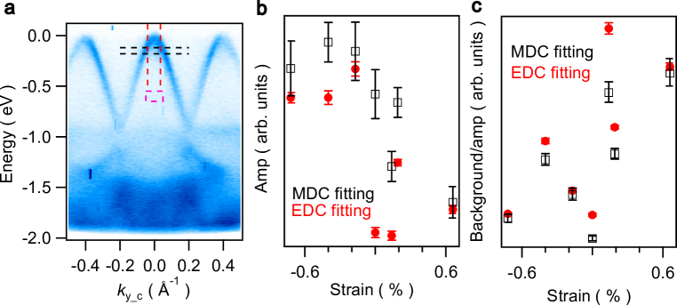
S8.8 Detailed analysis of ARPES data at different strains
Fig. S8 (b) and (c) indicate a decrease in the amplitude of the bands and an increase of background noise with tensile strain in HfTe5.