Large active-area superconducting microwire detector array with single-photon sensitivity in the near-infrared
Abstract
Superconducting nanowire single photon detectors (SNSPDs) are the highest-performing technology for time-resolved single-photon counting from the UV to the near-infrared. The recent discovery of single-photon sensitivity in micrometer-scale superconducting wires is a promising pathway to explore for large active area devices with application to dark matter searches and fundamental physics experiments. We present 8-pixel 1mm2 superconducting microwire single photon detectors (SMSPDs) with -wide wires fabricated from WSi and MoSi films of various stoichiometries using electron-beam and optical lithography. Devices made from all materials and fabrication techniques show saturated internal detection efficiency at 1064 nm in at least one pixel, and the best performing device made from silicon-rich WSi shows single-photon sensitivity in all 8 pixels and saturated internal detection efficiency in 6/8 pixels. This detector is the largest reported active-area SMSPD or SNSPD with near-IR sensitivity published to date, and the first report of an SMSPD array. By further optimizing the photolithography techniques presented in this work, a viable pathway exists to realize larger devices with cm2- scale active area and beyond.
I Introduction
Superconducting nanowire single photon detectors (SNSPDs) are a leading detector technology for time-correlated single photon counting from the UV to the near-infrared. They have become essential components in optical communication Biswas et al. (2017); Boroson et al. (2014); Li et al. (2020), Quantum Information Science Valivarthi et al. (2020); Takesue et al. (2007); Chen et al. (2008); Clausen et al. (2011); Stevens et al. (2010); Bussières et al. (2014); Shalm et al. (2015); Khasminskaya et al. (2016), and LIDAR McCarthy et al. (2013); Zhu et al. (2017); Chen et al. (2013); Zhou et al. (2015) experiments due to their unique combination of high timing resolution and high efficiency.
In recent years, the active areas of SNSPDs have steadily increased from the scale of a single-mode optical fiber diameter () towards the regime Wollman et al. (2019, 2021); Steinhauer, Gyger, and Zwiller (2021). As new applications for SNSPDs that leverage these large active areas emerge, there is a growing interest in exploring novel materials and device architectures. For applications in high energy physics such as dark matter (DM) searches, it is necessary to realize SNSPDs with larger active areas than the current state-of-the-art, by at least an order of magnitude. Scaling devices beyond the regime remains an open question that presents many challenges in terms of design, fabrication, and readout.
Traditional SNSPDs are comprised of nanowires with widths () meandered over the photoactive area and are fabricated using electron-beam lithography (EBL) to achieve the required resolution and optimal performance. Recent advances in the preparation of thin superconducting films have enabled the fabrication of a novel class of single-photon detectors with wire widths of several micrometers. We refer to these as superconducting microwire single-photon detectors (SMSPDs). In the near-IR, single-photon sensitivity in SMSPDs was first shown in niobium nitride (NbN) microstrips Korneeva et al. (2018) and shortly after in MoSi microstrip structures Korneeva et al. (2020). Following this, large area meander devices with saturated internal detection efficiency at were demonstrated in both silicon-rich tungsten silicide (WSi) Chiles et al. (2020) and molybdenum silicide (MoSi) Charaev et al. (2020), where the wire widths were on the order of 1-3 . UV detection at an elevated temperature of 3.4 K has also been demonstrated for large area MoSi SMSPDs Lita et al. (2021) and TaN SMSPDs have been developed for X-ray detection Yang et al. (2021). The timing resolution in NbN strips with widths up to Vodolazov et al. (2020) has been studied in a broad range of wavelengths and remains an important topic of fundamental research due to the complex role of vortex dynamics in the detection mechanism. Additionally, micron-scale wires are amenable to patterning with broadly available photolithography, which enables stable wafer-scale fabrication of devices. Direct laser writing has already been explored for micron-wide wires Protte et al. (2022), while the use of a deep-UV stepper is introduced in this work. Because of these developments, SMSPDs are promising to explore for -scale arrays in the future.
In this work, we investigate the feasibility a variety of materials for large active-area SMSPDs, including WSi of various stoichiometries and MoSi. An 8-pixel SMSPD array with meander geometry, -wide wires, 25 fill factor, and a total active area of 1 mm2 was fabricated from each material for comparison. The devices fabricated from WSi and MoSi films were patterned using EBL and photolithography, respectively. This work paves the way to realize cm2-active area devices which can have transformative capabilities in high energy physics.
The arrays fabricated in this work are a promising photosensor for a novel DM search experiment using cryogenic scintillating targets. Scintillating n-type GaAs doped with silicon and boron has recently been proposed as a target for detecting sub-GeV DM via electron recoils Derenzo et al. (2017, 2018, 2021). The emission bands of n-type GaAs are centered at 860 nm, 930 nm, 1070 nm, 1335 nm, with the 930 nm band having the highest luminosity. This application requires coupling the target to a single-photon detector with both near-IR sensitivity and a large active area to achieve high optical coupling efficiency. With this application in mind, the devices in this work were characterized at nm. The photoresponse at and dark count rates (DCR) were characterized at 0.8 K. Saturated internal detection efficiency at nm was achieved for all devices. The same mm2 array makes an ideal photosensor for new searches for axion- and dark photon-DM such as the BREAD experiment Liu et al. (2022). The proposed BREAD design consists of a cylindrical metal barrel for broadband conversion of DM into photons with an internal parabolic reflector that focuses the converted photons onto a photosensor with an active area of approximately 1 mm2. The current device with saturated internal detection efficiency at nm is able probe the unexplored region of parameter space with DM masses around 1.2 eV while meeting the active area requirements.
II Materials
Recent work by Xu et. al. Xu et al. (2021) demonstrates that NbN can be used in combination with an optical cavity to achieve a high system detection efficiency in small active area SMSPDs. WSi and MoSi are also promising materials for large active-area detectors since the films are amorphous and are thus expected to be very homogeneous.
A long saturation plateau in the photon count rate (PCR) curve allows for device operation at a bias current (), much lower than the detector critical current (), which decreases the amount of intrinsic detector dark counts. This can be achieved in a device by decreasing the density of charge carriers in the material, or by decreasing the superconducting energy gap of the material Colangelo et al. (2022). Decreasing the density of states reduces the number of Cooper pairs that need to be broken in order to weaken the superconducting state sufficiently for the nucleation of vortices. Once nucleated, vortices traverse the microwire and dissipate energy, which ultimately breaks the superconductivity across the whole microwire and leads to a detection event Vodolazov (2017). This enhancement in sensitivity can be achieved by increasing the material resistivity or by reducing the thickness of the film. Decreasing the superconducting gap of a material increases the number of quasiparticles that can be excited by a photon of a given energy. The gap energy is directly proportional to the critical temperature () of the device. In WSi, increasing the silicon content of the film both increases the resistivity and reduces Chiles et al. (2020); Verma et al. (2021); Colangelo et al. (2022).
One drawback of high resistivity materials is that the increased resistivity results in a larger kinetic inductance () of the material, which makes the recovery timescale of the device slower (, where is the load resistance). Additional challenges introduced by lowering of the device include a decreased output signal level, and a reduced operation temperature, which increases the level of complexity of the cryogenics.
We investigated 8-pixel meander SMSPD arrays made from three WSi films with different stoichiometries and thicknesses, and one made from a MoSi film. The sheet resistances were measured using a 4 probe setup at room temperature. The was defined as the temperature at the inflection point of the measured resistance–temperature curve. The composition of Film 1 was determined using Secondary Ion Mass Spectroscopy (SIMS), while Film 2 and 3 were analyzed using Rutherford Backscattering Spectrometry (EBS). The properties of the films are listed in table 1.
| Name | Substrate | Film | Stoichiometry (W:Si) | Thickness | Sheet Resistance | Fabrication | ||
|---|---|---|---|---|---|---|---|---|
| Film1 | Si | WSi | 52:48 | e-beam lithography | ||||
| Film2 | WSi | 70:30 | e-beam lithography | |||||
| Film3 | WSi | 42:58 | e-beam lithography | |||||
| Film4 | MoSi | unknown | photolithograpy |
Film 1 was co-sputtered from tungsten and silicon targets using the procedures outlined in Ref. Chiles et al. (2020). Films 2, 3 and 4 were deposited onto an oxidized Si(100) substrate with a -thick thermal oxide. Film 2 was sputtered from a target in an Ar atmosphere at a pressure of and a sputter power of . Film 3 was sputtered from a target in an Ar atmosphere at a pressure of and a sputter power of . Film 4 was made by co-sputtering process from Mo and Si targets in an argon atmosphere at a pressure of 2.5 mTorr. The Mo target was DC biased with a current of 130 mA, while 73 W of RF power was applied to the Si target.
III Design and Fabrication
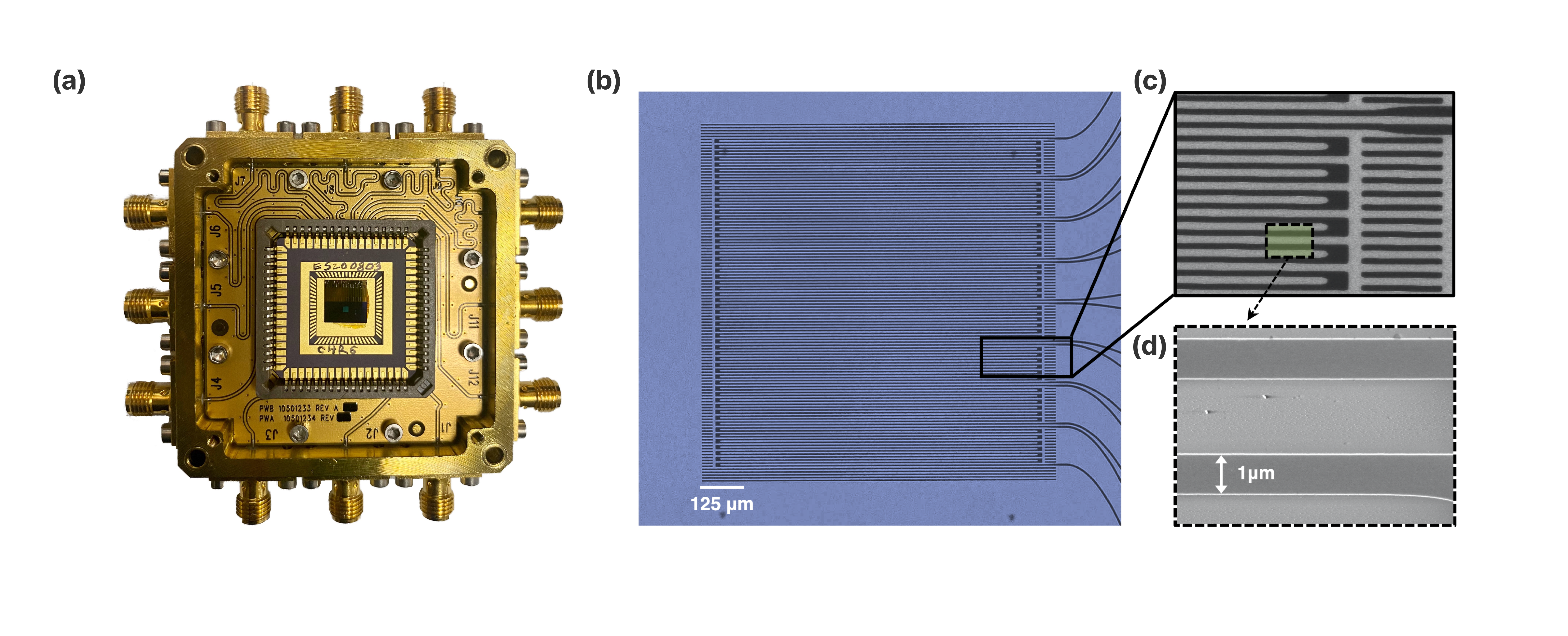
The SMSPDs in this work were designed as -wide meanders with a active area and a fill factor of 0.25. The area was chosen to be as large as possible while still fitting into a single write field of the EBL tool, to avoid stitching errors. The device was not put into a cavity, but a natural future extension of this work would be to embed the microwires in a standard, front-side illuminated cavity in order to increase the detection efficiency.
To investigate uniformity and yield, the detector was divided into pixels, each with an active area of . The pixels were designed with contact pads on either side, which enables the interconnection of all pixels in an arbitrary fashion and also allows for the use of differential readout Colangelo et al. (2021) if desired. In this work, we connected one side of each pixel to GND and the other to an individual readout line. In this single-ended configuration, the timing jitter of the Film 3 device was measured to be . Details on this measurement can be found in the supplementary information.
We patterned microwires with using EBL (Films 1,2,3) and optical lithography (Film 4). The EBL was done with the negative tone ma-N2401 resist at an acceleration voltage of and a dose of . The development was performed using AZ 300 MIF developer. The optical lithography was performed using a deep-UV stepper with a wavelength of in off-axis alignment mode. In addition, a backside anti-reflection coating (BARC) was used to prevent unwanted reflections from the wafer, which can cause a widening or constriction of the patterned wires. More details on the optical lithography of SNSPDs can be found in Beyer et al. (2015). In addition, dummy wires were added to either side of the active area for proximity effect correction to allow for a homogeneous exposure of the microwire pattern. The pattern was transferred via inductively-coupled plasma reactive-ion etching using and . After etching, the microwires were covered with of for passivation.
IV Readout
Typical readout of SNSPDs is based on room temperature, low-noise RF amplifiers with AC-coupling Marsili et al. (2013). An AC-coupled readout can prevent SNSPDs from reaching their maximum due to an early onset of latching Kerman et al. (2013). If the recovery timescale of the SNSPD is significantly longer than the timescale corresponding to the low-frequency cut-off of the amplifier, there is a significant undershoot in the readout signal, which results in additional current being sent to the detector during the recovery phase, causing the detector to latch. The low frequency cut-off of low-noise RF amplifiers is typically (), which is compatible with SNSPD recovery times (). In the case of the -wide wire devices in this work, the sheet-inductance is 650 pH/square and H for the device, thus the reset timescale is (). To overcome this limitation, we developed a DC-coupled amplifier based on a HEMT first stage, similar to the one described in Ref. Kerman et al. (2013), operating at . With the addition of a second stage SiGe amplifier, the total gain at is with a nominal bandwidth of 600 MHz. An overview diagram of the readout can be found in the supplemental information.
V Results
For characterization, the devices were cooled to a temperature of . The optical response was characterized with a pulsed laser at a wavelength of , attenuated to the single-photon level. The light was coupled to the detector using an SMF28 single-mode fiber.
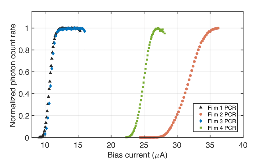
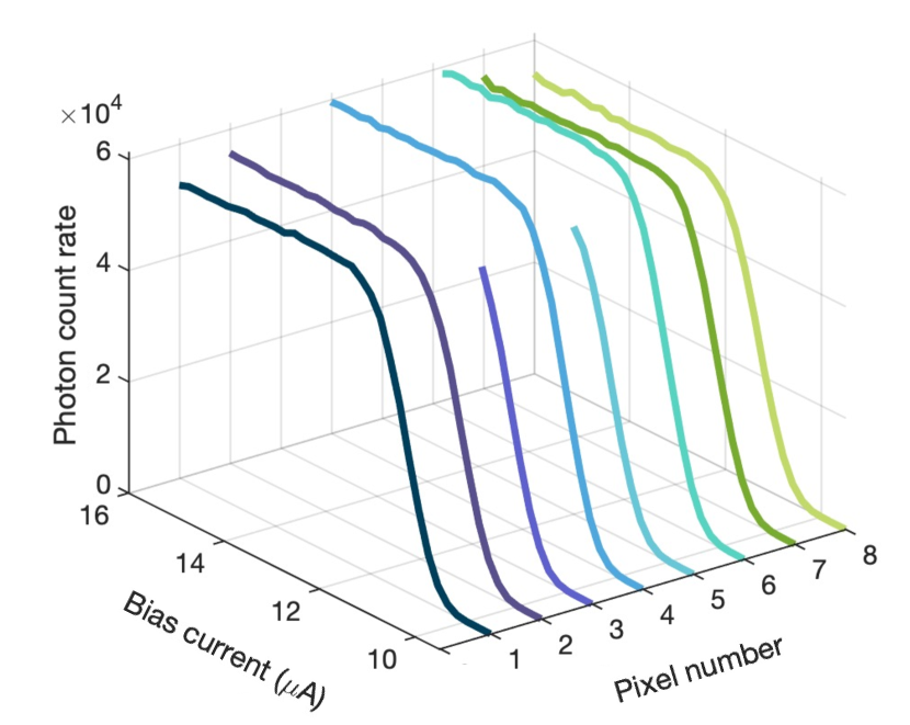
Detectors made from all investigated films using both EBL and optical lithography reach a saturation plateau (FIG. 2), with the longest plateau reached for devices made from Film 1 and Film 3 using EBL. The PCR as a function of for all 8 pixels of the best performing device (made from Film 3) is shown in figure 3. Six of the pixels display saturated internal detection efficiency; pixels 3 and 5 have suppressed switching currents, and they exhibit single-photon sensitivity at low but don’t reach a plateau.
.
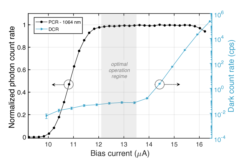
Figure 4 compares the DCR to the PCR as a function of for one of the pixels in the Film 3 device. The dark counts were recorded after implementing a lid to block stray light. The DCR at operational , determined to be the region in which the PCR is on the plateau with the lowest DCR ( to ), is cps.
In summary, all materials yielded functional detectors, and the detectors made from the films with the highest resistivity show the longest plateau. In addition, the detector made from Film 4 shows that large area SMSPDs can be fabricated with photolithography.
VI Discussion
All materials investigated in this work performed well and are viable approaches for future SMSPDs with active areas beyond . When operating a device, it is optimal to reach high fractions of the intrinsic depairing current Frasca et al. (2019), and it has been shown that the maximum achievable fraction of the depairing current (referred to as the constriction factor) is achieved when the operation temperature is Frasca et al. (2019); Colangelo et al. (2022). Thus, for a fixed operating temperature of 0.8 K, the optimal is expected to be 2.4 K, and further decreasing the of Film 3 is not feasible. To mitigate this, one option is to make devices from films which have a higher than Film 3 ( K compared to K), and decrease the film thickness to maintain the sensitivity.
The measured DCR in the Film 3 device has two distinct regions - the exponential portion at high , which is the expected intrinsic DCR scaling, and a plateau region at lower that approaches cps. The plateau suggests that background photons are reaching the active area, which can be mitigated via a more light-tight enclosure. For example, photons might be guided down the coaxial cables connected to the sample box (see Fig. 1). In future work, more light-tight enclosures will be investigated, to reach the expected intrinsic counts of the detector.
Since vortex crossing plays a crucial role in the detection mechanism for micron-wide SMSPDs Vodolazov (2017), the origin of intrinsic dark counts is expected to be thermally activated single-vortex crossing events Bulaevskii et al. (2011); Bulaevskii, Graf, and Kogan (2012), the rate of which has an exponential dependence on the bias current. We observe exponential behaviour of intrinsic dark counts in this work, in agreement with previous studies for narrower wires Bartolf et al. (2010); Yamashita et al. (2011). By extrapolating the exponential fit of the intrinsic DCR (see supplementary information Fig. 6), at the optimal operational bias current, it is expected to be - cps). We also note that operation at a lower temperature (0.8 K in this work) can significantly reduce the thermally-activated dark count events. This temperature dependence has been observed for narrow wires Bartolf et al. (2010); Yamashita et al. (2011), and operation at 0.3 K has been shown to lead to a cps dark count rate for 140 nm-wide WSi SNSPDs Chiles et al. (2022). Thus, similar performance is expected for SMSPDs in the future.
Another important component of reducing background counts is the implementation of coincidence monitoring between pixels, as this can be used as a veto for large events, such as cosmic rays, which is an additional motivation for multi-element arrays of SMSPDs. The observed timing resolution of 325 ps will enable such coincidence monitoring in the future.
Many developing applications for SNSPDs such as sub-GeV DM searches using n-type GaAs as cryogenic scintillating targets Derenzo et al. (2017, 2018, 2021); Derenzo (2022) and nanowires directly as target masses Hochberg et al. (2022) require large sensor active areas (cm2-scale) to realize a robust experiment Chou et al. (2022); Allmaras et al. (2021); Berggren et al. (2021). As a nanofabrication technique, the serial nature of EBL becomes unfeasible to write dense micron-scale patterns over large active areas, and the 1 mm2 devices are at the limit of EBL’s scope. Optical lithography allows for many microwire structures to be written in parallel, which greatly reduces the time and resources required to fabricate large pixels. Future work will focus on further optimizing the optical lithography processes implemented in this work, to scale to larger active areas. As the active areas are scaled in these devices, it will also be important to implement higher fill-factor designs that avoid performance degradation by current crowding effects in the bends. Known approaches to this include increasing the thickness of bends Xiong et al. (2022); Baghdadi et al. (2021) and placing bends outside of a high fill-factor active area Reddy et al. (2022). At 25% fill-factor and without an optical stack, the arrays characterized in this work have a system detection efficiency of approximately 4.2% (see supplemental information for details). Increasing the fill factor and embedding the microwires in an optical stack will increase the efficiency of the arrays significantly.
Another consideration toward cm2-scale active area arrays is the need for simultaneous readout of many channels. The direct, single-ended readout scheme employed in this work has been scaled to 64-pixel arrays Biswas et al. (2017); however, in the pursuit of cm2-scale devices with thousands of pixels, the high heat load associated with each readout channel and overall system complexity limit the scalability of this approach. The recently developed thermally-coupled imager (TCI) multiplexing architecture McCaughan et al. (2022) can be readily extended to devices with micron-scale wire widths and requires as few as 2 microwave readout lines to operate. The TCI architecture is particularly attractive for DM detection applications, where the overall maximum count rate of the experiment is low. Frequency domain multiplexing techniques have been demonstrated for 16-pixel SNSPDs with both DC and AC biasing schemes Doerner et al. (2017); Sinclair et al. (2019) and have superior current sensitivity, which is particularly important for SNSPDs with low energy thresholds approaching .
VII Conclusion
We fabricated 8 pixel, 1mm2 active area superconducting microwire single photon detector arrays with -wide wires from WSi films of various stoichiometries using EBL, and from MoSi using optical lithography to pattern the meander. All of these devices show single-photon sensitivity and saturated internal detection efficiency at nm. To our knowledge, this is the largest reported active area for an SMSPD or SNSPD with near-IR sensitivity to date, and the first report of an SMSPD array. In upcoming experiments, these arrays will be coupled to n-type GaAs crystals for scintillation lifetime and light yield measurements via optical and x-ray excitation.
This work elucidates a pathway to scale the active area of SMSPDs to the cm2 regime using optical lithography on high resistivity, amorphous films. These devices will have particular significance in low mass DM searches and other high energy physics applications. Future work will focus on developing large active area arrays with high system efficiency by implementing higher fill factor designs and integrating optical stacks to enhance absorption.
supplementary material
See supplementary material for more information on the experimental setup, readout, jitter and efficiency measurements, and intrinsic dark count rate.
Acknowledgements.
We would like to thank Richard Muller from Jet Propulsion Laboratory for the electron-beam lithography of our samples. Part of this research was performed at the Jet Propulsion Laboratory, California Institute of Technology, under contract with the National Aeronautics and Space Administration (80NM0018D0004). The authors acknowledge support from the JPL Strategic Research and Technology Development program, the DARPA Defense Sciences Office, and the Quantum Information Science Enabled Discovery (QuantISED) program for High Energy Physics (KA2401032). The authors are also grateful to Sahil Patel for his help in editing the final manuscript.Data Availability Statement
The data the support the findings of this study are openly available in Zenodo at https://doi.org/10.5281/zenodo.7644721 and available from the corresponding author upon reasonable request.
References
- Biswas et al. (2017) A. Biswas, M. Srinivasan, R. Rogalin, S. Piazzolla, J. Liu, B. Schratz, A. Wong, E. Alerstam, M. Wright, W. T. Roberts, J. Kovalik, G. Ortiz, A. Na-Nakornpanom, M. Shaw, C. Okino, K. Andrews, M. Peng, D. Orozco, and W. Klipstein, “Status of NASA’s deep space optical communication technology demonstration,” in 2017 IEEE International Conference on Space Optical Systems and Applications (ICSOS) (2017) p. 23.
- Boroson et al. (2014) D. M. Boroson, B. S. Robinson, D. V. Murphy, D. A. Burianek, F. Khatri, J. M. Kovalik, Z. Sodnik, and D. M. Cornwell, “Status of the Lunar Laser Communication Demonstration,” (SPIE International Society for Optics and Photonics Proceedings, 2014) p. 89710S.
- Li et al. (2020) X. Li, J. Tan, K. Zheng, L. Zhang, L. Zhang, W. He, P. Huang, H. Li, B. Zhang, Q. Chen, R. Ge, S. Guo, T. Huang, X. Jia, Q. Zhao, X. Tu, L. Kang, J. Chen, and P. Wu, “Enhanced photon communication through Bayesian estimation with an SNSPD array,” Photon. Res. 8, 637 (2020).
- Valivarthi et al. (2020) R. Valivarthi, S. I. Davis, C. Peña, S. Xie, N. Lauk, L. Narváez, J. P. Allmaras, A. D. Beyer, Y. Gim, M. Hussein, G. Iskander, H. L. Kim, B. Korzh, A. Mueller, M. Rominsky, M. Shaw, D. Tang, E. E. Wollman, C. Simon, P. Spentzouris, D. Oblak, N. Sinclair, and M. Spiropulu, “Teleportation systems toward a quantum internet,” PRX Quantum 1, 020317 (2020).
- Takesue et al. (2007) H. Takesue, S. W. Nam, Q. Zhang, R. H. Hadfield, T. Honjo, K. Tamaki, and Y. Yamamoto, “Quantum key distribution over a 40-dB channel loss using superconducting single-photon detectors,” Nature Photonics 1, 343 (2007).
- Chen et al. (2008) J. Chen, J. B. Altepeter, M. Medic, K. F. Lee, B. Gokden, R. H. Hadfield, S. W. Nam, and P. Kumar, “Demonstration of a quantum controlled-NOT gate in the telecommunications band,” Phys. Rev. Lett. 100, 133603 (2008).
- Clausen et al. (2011) C. Clausen, I. Usmani, F. Bussières, N. Sangouard, M. Afzelius, H. de Riedmatten, and N. Gisin, “Quantum storage of photonic entanglement in a crystal,” Nature 469, 508 (2011).
- Stevens et al. (2010) M. J. Stevens, B. Baek, E. A. Dauler, A. J. Kerman, R. J. Molnar, S. A. Hamilton, K. K. Berggren, R. P. Mirin, and S. W. Nam, “High-order temporal coherences of chaotic and laser light,” Opt. Express 18, 1430 (2010).
- Bussières et al. (2014) F. Bussières, C. Clausen, A. Tiranov, B. Korzh, V. B. Verma, S. W. Nam, F. Marsili, A. Ferrier, P. Goldner, H. Herrmann, C. Silberhorn, W. Sohler, M. Afzelius, and N. Gisin, “Quantum teleportation from a telecom-wavelength photon to a solid-state quantum memory,” Nature Photonics 8, 775 (2014).
- Shalm et al. (2015) L. K. Shalm, E. Meyer-Scott, B. G. Christensen, P. Bierhorst, M. A. Wayne, M. J. Stevens, T. Gerrits, S. Glancy, D. R. Hamel, M. S. Allman, K. J. Coakley, S. D. Dyer, C. Hodge, A. E. Lita, V. B. Verma, C. Lambrocco, E. Tortorici, A. L. Migdall, Y. Zhang, D. R. Kumor, W. H. Farr, F. Marsili, M. D. Shaw, J. A. Stern, C. Abellán, W. Amaya, V. Pruneri, T. Jennewein, M. W. Mitchell, P. G. Kwiat, J. C. Bienfang, R. P. Mirin, E. Knill, and S. W. Nam, “Strong loophole-free test of local realism,” Phys. Rev. Lett. 115, 250402 (2015).
- Khasminskaya et al. (2016) S. Khasminskaya, F. Pyatkov, K. Słowik, S. Ferrari, O. Kahl, V. Kovalyuk, P. Rath, A. Vetter, F. Hennrich, M. M. Kappes, G. Gol’tsman, A. Korneev, C. Rockstuhl, R. Krupke, and W. H. P. Pernice, “Fully integrated quantum photonic circuit with an electrically driven light source,” Nature Photonics 10, 727 (2016).
- McCarthy et al. (2013) A. McCarthy, N. J. Krichel, N. R. Gemmell, X. Ren, M. G. Tanner, S. N. Dorenbos, V. Zwiller, R. H. Hadfield, and G. S. Buller, “Kilometer-range, high resolution depth imaging via 1560 nm wavelength single-photon detection,” Opt. Express 21, 8904 (2013).
- Zhu et al. (2017) J. Zhu, Y. Chen, L. Zhang, X. Jia, Z. Feng, G. Wu, X. Yan, J. Zhai, Y. Wu, Q. Chen, Z. W. Xiaoying Zhou, C. Zhang, L. Kang, J. Chen, and P. Wu, “Demonstration of measuring sea fog with an snspd-based Lidar system,” Scientific Reports 7, 15113 (2017).
- Chen et al. (2013) S. Chen, D. Liu, W. Zhang, L. You, Y. He, W. Zhang, X. Yang, G. Wu, M. Ren, H. Zeng, Z. Wang, X. Xie, and M. Jiang, “Time-of-flight laser ranging and imaging at 1550 nm using low-jitter superconducting nanowire single-photon detection system,” Appl. Opt. 52, 3241 (2013).
- Zhou et al. (2015) H. Zhou, Y. He, L. You, S. Chen, W. Zhang, J. Wu, Z. Wang, and X. Xie, “Few-photon imaging at 1550 nm using a low-timing-jitter superconducting nanowire single-photon detector,” Opt. Express 23, 14603 (2015).
- Wollman et al. (2019) E. E. Wollman, V. B. Verma, A. E. Lita, W. H. Farr, M. D. Shaw, R. P. Mirin, and S. W. Nam, “Kilopixel array of superconducting nanowire single-photon detectors,” Opt. Express 27, 35279 (2019).
- Wollman et al. (2021) E. E. Wollman, V. B. Verma, A. B. Walter, J. Chiles, B. Korzh, J. P. Allmaras, Y. Zhai, A. E. Lita, A. N. McCaughan, E. Schmidt, S. Frasca, R. P. Mirin, S. W. Nam, and M. D. Shaw, “Recent advances in superconducting nanowire single-photon detector technology for exoplanet transit spectroscopy in the mid-infrared,” Journal of Astronomical Telescopes, Instruments and Systems 7, 011004 (2021).
- Steinhauer, Gyger, and Zwiller (2021) S. Steinhauer, S. Gyger, and V. Zwiller, “Progress on large-scale superconducting nanowire single-photon detectors,” Applied Physics Letters 118, 100501 (2021).
- Korneeva et al. (2018) Y. P. Korneeva, D. Y. Vodolazov, A. V. Semenov, I. N. Florya, N. Simonov, E. Baeva, A. A. Korneev, G. N. Goltsman, and T. M. Klapwijk, “Optical single-photon detection in micrometer-scale NbN bridges,” Phys. Rev. Appl. 9, 064037 (2018).
- Korneeva et al. (2020) Y. P. Korneeva, N. Manova, I. Florya, M. Y. Mikhailov, O. Dobrovolskiy, A. Korneev, and D. Y. Vodolazov, “Different single-photon response of wide and narrow superconducting strips,” Phys. Rev. Appl. 13, 024011 (2020).
- Chiles et al. (2020) J. Chiles, S. M. Buckley, A. Lita, V. B. Verma, J. Allmaras, B. Korzh, M. D. Shaw, J. M. Shainline, R. P. Mirin, and S. W. Nam, “Superconducting microwire detectors based on WSi with single-photon sensitivity in the near-infrared,” Applied Physics Letters 116, 242602 (2020).
- Charaev et al. (2020) I. Charaev, Y. Morimoto, A. Dane, A. Agarwal, M. Colangelo, and K. K. Berggren, “Large-area microwire MoSi single-photon detectors at 1550 nm wavelength,” Applied Physics Letters 116, 242603 (2020).
- Lita et al. (2021) A. E. Lita, V. B. Verma, J. Chiles, R. P. Mirin, and S. W. Nam, “MoxSi1-x a versatile material for nanowire to microwire single-photon detectors from UV to near IR,” Superconductor Science and Technology 34, 054001 (2021).
- Yang et al. (2021) C. Yang, M. Si, X. Zhang, A. Yu, J. Huang, Y. Pan, H. Li, L. Li, Z. Wang, S. Zhang, J. Xia, Z. Liu, H. Guo, and L. You, “Large-area TaN superconducting microwire single photon detectors for x-ray detection,” Opt. Express 29, 21400 (2021).
- Vodolazov et al. (2020) D. Vodolazov, N. Manova, Y. Korneeva, and A. Korneev, “Timing jitter in NbN superconducting microstrip single-photon detector,” Phys. Rev. Applied 14, 044041 (2020).
- Protte et al. (2022) M. Protte, V. B. Verma, J. P. Höpker, R. P. Mirin, S. W. Nam, and T. J. Bartley, “Laser-lithographically written micron-wide superconducting nanowire single-photon detectors,” Superconductor Science and Technology 35, 055005 (2022).
- Derenzo et al. (2017) S. Derenzo, R. Essig, A. Massari, A. Soto, and T.-T. Yu, “Direct detection of sub-gev dark matter with scintillating targets,” Phys. Rev. D 96, 016026 (2017).
- Derenzo et al. (2018) S. Derenzo, E. Bourret, S. Hanrahan, and G. Bizarri, “Cryogenic scintillation properties of n-type GaAs for the direct detection of mev/c2 dark matter,” Journal of Applied Physics 123, 114501 (2018).
- Derenzo et al. (2021) S. Derenzo, E. Bourret, C. Frank-Rotsch, S. Hanrahan, and M. Garcia-Sciveres, “How silicon and boron dopants govern the cryogenic scintillation properties of n-type GaAs,” Nuclear Instruments and Methods in Physics Research Section A: Accelerators, Spectrometers, Detectors and Associated Equipment 989, 164957 (2021).
- Liu et al. (2022) J. Liu, K. Dona, G. Hoshino, S. Knirck, N. Kurinsky, M. Malaker, D. W. Miller, A. Sonnenschein, M. H. Awida, P. S. Barry, K. K. Berggren, D. Bowring, G. Carosi, C. Chang, A. Chou, R. Khatiwada, S. Lewis, J. Li, S. W. Nam, O. Noroozian, and T. X. Zhou (BREAD Collaboration), “Broadband solenoidal haloscope for terahertz axion detection,” Phys. Rev. Lett. 128, 131801 (2022).
- Xu et al. (2021) G.-Z. Xu, W.-J. Zhang, L.-X. You, J.-M. Xiong, X.-Q. Sun, H. Huang, X. Ou, Y.-M. Pan, C.-L. Lv, H. Li, Z. Wang, and X.-M. Xie, “Superconducting microstrip single-photon detector with system detection efficiency over 90% at 1550 nm,” Photonics Research 9, 958 (2021).
- Colangelo et al. (2022) M. Colangelo, A. B. Walter, B. A. Korzh, E. Schmidt, B. Bumble, A. E. Lita, A. D. Beyer, J. P. Allmaras, R. M. Briggs, A. G. Kozorezov, E. E. Wollman, M. D. Shaw, and K. K. Berggren, “Large-area superconducting nanowire single-photon detectors for operation at wavelengths up to 7.4 m,” Nano Lett. 22, 5667 (2022).
- Vodolazov (2017) D. Y. Vodolazov, “Single-Photon detection by a dirty Current-Carrying superconducting strip based on the Kinetic-Equation approach,” Physical Review Applied 7, 034014 (2017).
- Verma et al. (2021) V. B. Verma, B. Korzh, A. B. Walter, A. E. Lita, R. M. Briggs, M. Colangelo, Y. Zhai, E. E. Wollman, A. D. Beyer, J. P. Allmaras, H. Vora, D. Zhu, E. Schmidt, A. G. Kozorezov, K. K. Berggren, R. P. Mirin, S. W. Nam, and M. D. Shaw, “Single-photon detection in the mid-infrared up to 10 µ m wavelength using tungsten silicide superconducting nanowire detectors,” APL Photonics 6, 056101 (2021).
- Colangelo et al. (2021) M. Colangelo, B. Korzh, J. P. Allmaras, A. D. Beyer, A. S. Mueller, R. M. Briggs, B. Bumble, M. Runyan, M. J. Stevens, A. N. McCaughan, D. Zhu, S. Smith, W. Becker, L. Narváez, J. C. Bienfang, S. Frasca, A. E. Velasco, C. H. Peña, E. E. Ramirez, A. B. Walter, E. Schmidt, E. E. Wollman, M. Spiropulu, R. Mirin, S. W. Nam, K. K. Berggren, and M. D. Shaw, “Impedance-matched differential superconducting nanowire detectors,” arXiv:2108.07962 (2021).
- Beyer et al. (2015) A. D. Beyer, M. D. Shaw, F. Marsili, M. S. Allman, A. E. Lita, V. B. Verma, G. V. Resta, J. A. Stern, R. P. Mirin, S. W. Nam, and W. H. Farr, “Tungsten silicide superconducting nanowire single-photon test structures fabricated using optical lithography,” IEEE Transactions on Applied Superconductivity 25, 1 (2015).
- Marsili et al. (2013) F. Marsili, V. B. Verma, J. A. Stern, S. Harrington, A. E. Lita, T. Gerrits, I. Vayshenker, B. Baek, M. D. Shaw, R. P. Mirin, and S. W. Nam, “Detecting single infrared photons with 93% system efficiency,” Nature Photonics 7, 210 (2013).
- Kerman et al. (2013) A. J. Kerman, D. Rosenberg, R. J. Molnar, and E. A. Dauler, “Readout of superconducting nanowire single-photon detectors at high count rates,” Journal of Applied Physics 113, 144511 (2013).
- Frasca et al. (2019) S. Frasca, B. Korzh, M. Colangelo, D. Zhu, A. E. Lita, J. P. Allmaras, E. E. Wollman, V. B. Verma, A. E. Dane, E. Ramirez, A. D. Beyer, S. W. Nam, A. G. Kozorezov, M. D. Shaw, and K. K. Berggren, “Determining the depairing current in superconducting nanowire single-photon detectors,” Phys. Rev. B 100, 054520 (2019).
- Bulaevskii et al. (2011) L. N. Bulaevskii, M. J. Graf, C. D. Batista, and V. G. Kogan, “Vortex-induced dissipation in narrow current-biased thin-film superconducting strips,” Phys. Rev. B: Condens. Matter Mater. Phys. 83, 144526 (2011).
- Bulaevskii, Graf, and Kogan (2012) L. N. Bulaevskii, M. J. Graf, and V. G. Kogan, “Vortex-assisted photon counts and their magnetic field dependence in single-photon superconducting detectors,” Phys. Rev. B: Condens. Matter Mater. Phys. 85, 014505 (2012).
- Bartolf et al. (2010) H. Bartolf, A. Engel, A. Schilling, K. Il’in, M. Siegel, H.-W. Hübers, and A. Semenov, “Current-assisted thermally activated flux liberation in ultrathin nanopatterned NbN superconducting meander structures,” Phys. Rev. B: Condens. Matter Mater. Phys. 81, 024502 (2010).
- Yamashita et al. (2011) T. Yamashita, S. Miki, K. Makise, W. Qiu, H. Terai, M. Fujiwara, M. Sasaki, and Z. Wang, “Origin of intrinsic dark count in superconducting nanowire single-photon detectors,” Appl. Phys. Lett. 99, 161105 (2011).
- Chiles et al. (2022) J. Chiles, I. Charaev, R. Lasenby, M. Baryakhtar, J. Huang, A. Roshko, G. Burton, M. Colangelo, K. Van Tilburg, A. Arvanitaki, S. W. Nam, and K. K. Berggren, “New constraints on dark photon dark matter with superconducting nanowire detectors in an optical haloscope,” Phys. Rev. Lett. 128, 231802 (2022).
- Derenzo (2022) S. E. Derenzo, “Monte carlo calculations of the extraction of scintillation light from cryogenic n-type GaAs,” Nuclear Instruments and Methods in Physics Research Section A: Accelerators, Spectrometers, Detectors and Associated Equipment 1034, 166803 (2022).
- Hochberg et al. (2022) Y. Hochberg, B. V. Lehmann, I. Charaev, J. Chiles, M. Colangelo, S. W. Nam, and K. K. Berggren, “New constraints on dark matter from superconducting nanowires,” Phys. Rev. D 106, 112005 (2022).
- Chou et al. (2022) A. S. Chou, M. Soares-Santos, T. M. P. Tait, R. X. Adhikari, L. A. Anchordoqui, J. Annis, C. L. Chang, J. Cooley, A. Drlica-Wagner, K. Fang, B. Flaugher, J. Jaeckel, W. H. Lippincott, V. Miranda, L. Newburgh, J. A. Newman, C. Prescod-Weinstein, G. Rybka, B. S. Sathyaprakash, D. J. Schlegel, D. M. S. T. R. Slatyer, A. Slosar, K. Tollefson, L. Winslow, H.-B. Yu, T.-T. Yu, K. Engel, S. Gardner, T. R. Lewis, B. Shakya, and P. Tanedo, “Snowmass cosmic frontier report,” arXiv , arXiv:2211.09978 (2022).
- Allmaras et al. (2021) J. Allmaras, K. Berggren, I. Charaev, C. Chang, J. Chiles, B. Korzh, A. Lita, J. Luskin, S. W. Nam, V. Novosad, and et al., “Superconducting nanowire single-photon detectors,” Snowmass2021 - Letter of Interest (2021).
- Berggren et al. (2021) K. Berggren, E. Bourret-Courchesne, S. Derenzo, R. Essig, M. Garcia-Sciveres, B. Korzh, N. Kurinsky, S. W. Nam, J. Luskin, D. McKinsey, and et al., “A scintillating n-type GaAs detector for sub-gev dark matter direct detection,” Snowmass2021 - Letter of Interest (2021).
- Xiong et al. (2022) J.-M. Xiong, W.-J. Zhang, G.-Z. Xu, L.-X. You, X.-Y. Zhang, L. Zhang, C.-J. Zhang, D.-H. Fan, Y.-Z. Wang, H. Li, and Z. Wang, “Reducing current crowding in meander superconducting strip single-photon detectors by thickening bends,” Superconductor Science and Technology 35, 055015 (2022).
- Baghdadi et al. (2021) R. Baghdadi, E. Schmidt, S. Jahani, I. Charaev, M. G. W. Müller, M. Colangelo, D. Zhu, K. Ilin, A. D. Semenov, Z. Jacob, M. Siegel, and K. K. Berggren, “Enhancing the performance of superconducting nanowire-based detectors with high-filling factor by using variable thickness,” Superconductor Science and Technology 34, 035010 (2021).
- Reddy et al. (2022) D. V. Reddy, N. Otrooshi, S. W. Nam, R. P. Mirin, and V. B. Verma, “Broadband polarization insensitivity and high detection efficiency in high-fill-factor superconducting microwire single-photon detectors,” APL Photonics 7, 051302 (2022).
- McCaughan et al. (2022) A. N. McCaughan, Y. Zhai, B. Korzh, J. P. Allmaras, B. G. Oripov, M. D. Shaw, and S. W. Nam, “The thermally coupled imager: A scalable readout architecture for superconducting nanowire single photon detectors,” Applied Physics Letters 121, 102602 (2022).
- Doerner et al. (2017) S. Doerner, A. Kuzmin, S. Wuensch, I. Charaev, F. Boes, T. Zwick, and M. Siegel, “Frequency-multiplexed bias and readout of a 16-pixel superconducting nanowire single-photon detector array,” Applied Physics Letters 111, 032603 (2017).
- Sinclair et al. (2019) A. K. Sinclair, E. Schroeder, D. Zhu, M. Colangelo, J. Glasby, P. D. Mauskopf, H. Mani, and K. K. Berggren, “Demonstration of microwave multiplexed readout of DC-biased superconducting nanowire detectors,” IEEE Transactions on Applied Superconductivity 29, 1 (2019).
Supplementary Information
March 18, 2023
1. Readout
The biasing and readout scheme is shown in figure 1. The signal from each microwire was connected to a cryogenic readout board at 40 K containing a resistive bias-tee and the two-stage cryogenic amplifier (DC-coupled HEMT and SiGe LNA).
![[Uncaptioned image]](/html/2303.10739/assets/x4.png)
The SMSPD is represented as a variable resistor in series with an inductor with kinetic inductance . encodes the time-dependent resistance of the normal domain following the absorption of a photon and formation of a hotspot.
2. Efficiency Measurements
The efficiency of the Film 3 device was characterized using the setup depicted in figure 2 according to a procedure similar to those of references [1] and [2] . photons from a mode-locked fiber laser were sent into a fiber beam splitter. A power meter (PM 1) was connected to one output of a 90:10 fiber beam splitter (BS) to monitor power fluctuations in the laser. Light from the signal output of the beamsplitter was collimated and directed through three attenuator wheels consisting of various neutral density (ND) filters, and then coupled into a single fiber patch cable via a collimator. The attenuation factor corresponding to each ND filter was measured at nm using a calibrated power meter (PM 2). Linearity was verified with combinations of different ND filters at high power measured by PM 2, shown in figure 3.
![[Uncaptioned image]](/html/2303.10739/assets/x5.png)
After calibration, the light was attenuated down to the single-photon level and a known quantity of photons were delivered into the cryostat to illuminate the SMSPD. The transmission of this SMF-28 fiber at was also calibrated. On the lid of the SMSPD, the collimated beam passes through an aspheric lens with a nominal focal length of 15 mm. Losses through these optics were calibrated, and the lens was placed out of focus to increase the spot size illuminating the detector, to approximately .
![[Uncaptioned image]](/html/2303.10739/assets/x6.png)
The SDE reaches . The uncertainty of the power meters was estimated by calculating the standard error of the mean of 10 consecutive measurements on 4 different power meter heads. This was determined to be . The total SDE error is therefore .
3. Jitter Measurements
The timing jitter of the Film 3 array at nm was characterized by measuring the instrument response function (IRF). The output of the mode locked laser with repition rate was attenuated to the single photon level by a fiber variable optical attenuator (VOA). Timing reference pulses were generated by a fast photodiode and sent to the “Stop” port of a commercial time-correlated single-photon counting (TCSPC) module (Becker-Hickl, SPC-150). The amplified voltage output pulses of the SMSPD were sent to the "Start” port of the SPC-150, which then builds a statistical distribution of the intervals between the “Start” and the “Stop” signals. The setup is depicted in figure 4.
![[Uncaptioned image]](/html/2303.10739/assets/x7.png)
The IRF (jitter histogram) for one pixel of the the Film 3 array is shown in figure 5 for a bias current of . The jitter is defined as the FWHM of the IRF and was measured to be .
![[Uncaptioned image]](/html/2303.10739/assets/x8.png)
4. Intrinsic Dark Count Rate Estimate
The portion of the measured Film 3 DCR at has the expected exponential scaling of the intrinsic device DCR. The plateau region at is background-limited and thus a few orders of magnitude higher than the expected intrinsic DCR. To estimate the intrinsic DCR at the optimal for operation (12.2 - ), an exponential function was fit to the data at and extrapolated to lower . The best fit exponential function predicts an intrinsic DCR of at the lower bound of this operational regime () and a DCR of at the upper bound of this operational regime (). We expect to be able to reach these levels by implementing a more light-tight detector enclosure, while operating at a lower temperature (e.g. 0.3 K) could reduce the DCR to below the level.
![[Uncaptioned image]](/html/2303.10739/assets/x9.png)
References
-
[1]
E. E. Wollman, V. B. Verma, A. D. Beyer, R. M. Briggs, B. Korzh, J. P. Allmaras, F. Marsili, A. E. Lita, R. P. Mirin, S. W. Nam, and M. D. Shaw. UV superconducting nanowire single-photon detectors with high efficiency, low noise, and 4K operating temperature. Opt. Express, 25(22):26792–26801, 2017.
-
[2]
D. V. Reddy, N. Otrooshi, S. Nam, R. P. Mirin, and V.B. Verma. Broadband polar- ization insensitivity and high detection efficiency in high-fill-factor superconducting microwire single-photon detectors. APL Photonics, 7(5):051302, 2022.