Disentangling superconductor and dielectric microwave losses in sub-micron Nb/TEOS-SiO2 interconnects using a multi-mode microstrip resonator
Abstract
Understanding the origins of power loss in superconducting interconnects is essential for the energy efficiency and scalability of superconducting digital logic. At microwave frequencies, power dissipates in both the dielectrics and superconducting wires, and these losses can be of comparable magnitude. A novel method to accurately disentangle such losses by exploiting their frequency dependence using a multi-mode transmission line resonator, supported by a geometric factor concept and a 3D superconductor finite element method (FEM) modeling, is described. Using the method we optimized a planarized fabrication process of reciprocal quantum logic (RQL) for the interconnect loss at 4.2 K and GHz frequencies. The interconnects are composed of niobium (Nb) insulated by silicon dioxide made with a tetraethyl orthosilicate precursor (TEOS-SiO2). Two process generations use damascene fabrication, and the third one uses Cloisonné fabrication. For all three, TEOS-SiO2 exhibits a dielectric loss tangent , independent of Nb wire width over . The Nb loss varies with both the processing and the wire width. For damascene fabrication, scanning transmission electron microscopy (STEM) and energy dispersive X-ray spectroscopy (EDS) reveal that Nb oxide and Nb grain growth orientation increase the loss above the Bardeen–Cooper–Schrieffer (BCS) minimum theoretical resistance . For Cloisonné fabrication, the wide Nb wires exhibit an intrinsic resistance at 10 GHz, which is below . That is arguably the lowest resistive loss reported for Nb.
I Introduction
Superconducting single flux quantum (SFQ) logic relies on Josephson junctions to form the logic gates, and superconducting transmission lines to deliver clock and power to the gates as well as to propagate bits of information between various circuits on the chip. [1, 2, 3, 4, 5, 6] The bits are encoded into pulses of picosecond duration and millivolt amplitude, which are generated by the junctions[7] and each carry a magnetic flux quantum . With the pulse energy of , where is the junction critical current, and the available clock speed up to 120 GHz,[8] to compete with CMOS-based computing technologies, the SFQ logic community has been focused on the energy efficiency and scalability. [9]
Energy efficient SFQ logic families include quantum flux parametron (QFP),[3] reciprocal quantum logic (RQL), [4] energy efficient single flux quantum (eSFQ) logic,[5] and adiabatic quantum flux parametron (AQFP).[6] Analogous to Cu/low-k interconnects dominating the net CMOS power budget,[10] superconducting interconnects can notably impact the energy efficiency of SFQ logic. For instance, AC-powered RQL has been reported to be 300 times more energy efficient than CMOS, including the cooling overhead in large-scale systems.[4] However, a metamaterial zeroth order resonator (ZOR) delivering clock and power to RQL gates at GHz frequencies dissipated twice more power than the logic junctions, due to the loss in transmission lines forming the ZOR.[11]
Interconnect density remains one of the main factors limiting the scalability of all forms of superconducting logic.[12] The performance capability of an SFQ logic chip increases with the total number of logic gates, which calls for more interconnect layers with smaller wire width and spacing (pitch). Reducing the wire cross-section to deep sub-micron dimensions, where it becomes comparable to or smaller than the superconductor magnetic penetration depth in Nb, creates complex requirements to fabricate high-bandwidth, low-loss interconnects. Chemical mechanical polishing or planarization (CMP) [13] allows one to fabricate an SFQ logic chip with up to ten wiring layers, [14] by removing topography left from the previous layer patterning and deposition.[15, 16, 17] In our work, both the damascene (metal CMP) and Cloisonné (dielectric CMP) planarized processes will be utilized and compared. We will present an elemental material analysis to reveal possible sources of extrinsic microwave loss in the sub-micron Nb interconnects.
The microstrip transmission line (MTL) and stripline are the ubiquitous superconducting interconnects, with 700 GHz analog bandwidth. On one hand, they can provide a basic building block for GHz clock and power distribution systems.[18, 19, 11] On the other hand, they can form a passive transmission line, to propagate low-bandwidth (35-50 GHz) data with 7-10 SFQ pulses per bit,[19] or to propagate high-bandwidth (350 GHz) data with single SFQ pulse per bit,[20, 21] or to produce a delay-line memory. [22] The power dissipation is governed by the superconductor and dielectric loss, and is inversely proportional to a transmission line resonator figure of merit, quality factor (Q-factor).[23] Similarly, the propagation distance of SFQ pulse scales with the Q-factor.[21] Our paper is concerned with simultaneously extracting the superconductor microwave resistance and the insulator loss tangent from experimental Q-factor data on MTL resonators, at an RQL operating temperature of liquid helium (LHe) .
Resonant structures provide the most sensitive way to measure [24, 25, 26, 27, 28, 29, 30, 31, 32, 33, 34] and [35, 36, 37, 38, 39] at microwave frequencies. We shall employ finite-length sections of MTL, with open-circuit boundary conditions at the ends, to act as MTL resonators, enabling sensitive measurements of loss and inductance.[40, 41, 42, 43, 44] A resonator Q-factor is defined as , where is the resonant frequency, is the energy stored in the resonator, and is the net power lost by the resonator. In practice, one measures the loaded Q-factor
| (1) |
where is the internal (unloaded) Q-factor, is the external (coupling) Q-factor associated with the resonator excitation, and , and are the partial Q-factors associated with the conductor, dielectric and radiation power loss, respectively. The coupling contribution can be removed by modern analysis techniques.[45, 46] The radiation loss[47] is typically negligibly small and can be ignored. Since and are additive, the corresponding conductor and dielectric loss contributions are inseparable. To disentangle them, resonant techniques either postulate the “unwanted” loss, or exploit regimes where is dominated by the “wanted” loss. The regime favors the measurement of . The regime favors the measurement of .
Superconducting cavity [24, 25, 28, 29] and quasi-optical[31] resonators measure of bulk and thin-film superconductors by attaining . To deduce of superconducting thin films using a dielectric resonator technique,[32] one must presume a value for the dielectric puck. Tuckerman et al. measured of Nb/polyimide flexible transmission line tapes in the regime, at 1.2 K and 20 mK where the Nb loss becomes negligible.[38] Quantum computing resonators attain at mK temperatures, to characterize a two-level-system dielectric loss.[39] Kaiser exploited in the Nb lumped element resonator, to investigate frequency dependence of for amorphous thin-film dielectrics at 4.2 K.[37] Oates et al. reported that at 4 K, losses in Nb/SiO2 sub-micron stripline resonators are limited by the dielectric except for the narrowest strips, although they did not deduce or .[48] Krupka et al. optimized a dielectric resonator for , to measure the loss tangent of isotropic low-loss dielectrics [36] and high-resistivity silicon[49] at room temperature. Taber overcame the above limitations by varying the dielectric spacer thickness (geometric factor) of the superconducting parallel-plate resonator,[30] which allows to deduce both and .[30, 33] However, this approach is impractical for characterization of patterned interconnects.
In contrast to existing work, we shall extract both the superconductor and dielectric loss by exploiting their frequency dependence in a multi-mode MTL resonator. In fact, we shall take advantage of both losses in our structures being of comparable magnitude , owing to interplay between the MTL geometry and loss. Fitting theoretical model to experimental dependence of on the resonant frequency allows us to quantitatively de-convolve the two losses in a single measurement.
Analytical or numerical modeling of superconducting interconnects[20, 50, 51, 52, 53, 54] typically relies on the Leontovich boundary condition, commonly referred to as a surface impedance boundary condition (SIBC).[55, 56, 57, 58] It approximates the transmitted wave as a wave propagating normal to the surface of an imperfect conductor, regardless of the incident angle. SIBC is immensely fruitful for electrically-large systems[25, 59, 26, 32, 28, 33, 34] with the conductor surface curvature radius much greater than the penetration depth . The SIBC approximation is inapplicable to an interconnect with the cross-section comparable to or smaller than .
To overcome this limitation for submicron MTLs, we shall deal the intrinsic impedance , where is the microwave reactance, is the vacuum permeability, is the angular frequency with being the linear frequency, and is the superconductor complex conductivity.[60] A finite element method (FEM) simulation can provide the field and current distributions within the wire,[61, 21] which for a good superconductor of , or , are defined by the superfluid electrons distribution, that is or . This allows us to derive a relationship between and via a geometric factor defined by the MTL cross-section and . Simulating the MTL geometric factor using Ansys’ 3D electromagnetic FEM modeler,[62] we investigate and as functions of Nb wire width down to . FEM modeling can also address the fabrication effects impacting interconnects, such as irregular cross-section shape and rounded edges of the wire, critical dimensions miss-targeting and variation across the wafer, intermixing of materials at the interface, etc.
This paper is organized as follows. First, we will describe design, fabrication, and RF characterization of a multi-mode MTL resonator. After presenting data for the frequency dependence of internal Q-factor, we will introduce analytical theory to fit them. Next, a resonator geometric factor, involved into the theory, will be obtained from 3D FEM simulations. Finally, the superconductor and dielectric losses will be deduced, and their dependence on the MTL width and processing conditions will be discussed with the aid of a microscopic analysis.
II Resonator design, fabrication, and characterization
II.1 Design and layout
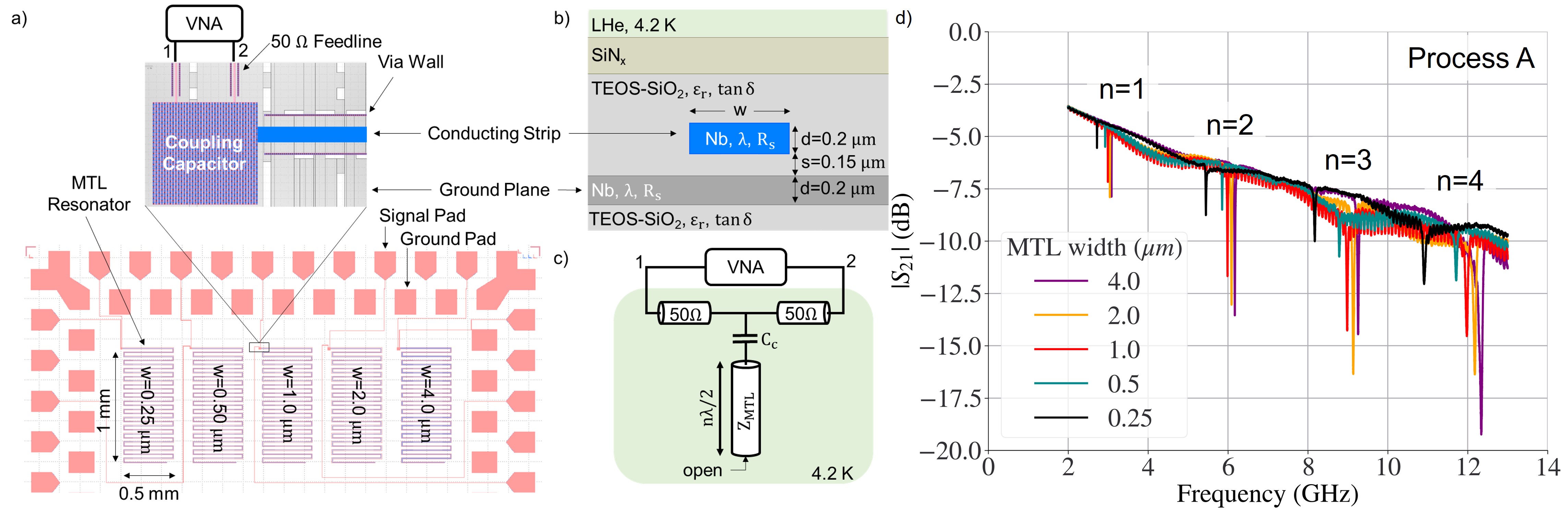
To implement the proposed concept, we designed a chip containing five half-wavelength-long open-ended MTL resonators shown in Fig. 1(a), representative of RQL interconnects. The MTL is formed by a Nb ground plane and a Nb conducting strip, embedded into silicon dioxide derived from tetraethyl orthosilicate (TEOS-SiO2), as depicted in Fig. 1(b). The conducting strip width varies from 0.25 to . Each resonator is folded into a meander shape to conserve space. Via walls surround the conducting strip, to facilitate RF isolation between the adjacent meander sections.
A superconducting MTL supports a slow wave.[63, 64] A resonant condition yields the MTL resonator eigen frequencies
| (2) |
where is the phase constant, is the resonator geometrical length, is the longitudinal mode index, and and are the series inductance and shunt capacitance per unit length given in Appendix A, Eqs. 15b and 15d. The approximation on the right in Eq. 2 holds for a wide MTL (parallel-plate waveguide) with , where is the dielectric spacing between the strip and ground plane,[33] is the speed of light in vacuum, is the relative dielectric constant, and is the superconductor wire thickness. The resonator frequency was designed based upon the material nominal properties (, ) and fabrication thicknesses (, ) shown in Fig. 1(b). The selected resonator length is a trade-off between fitting many resonators on a single chip, and accommodating many resonant modes within the test setup bandwidth. With the above parameters, Eq. 2 predicts a fundamental frequency . That frequency, measured for a resonator, is , which is within 0.8% of the above estimate. This agreement supports our assumed values of for TEOS-SiO2,[65] and for Nb. The latter was verified by SQUID inductance measurements[66] and agrees with Ref.[67]
Each resonator is reactively coupled to a microstrip feedline through a coupling capacitor, as shown in Fig. 1(a) zoom-in. Figure 1(c) conceptualizes the RF driving network for our resonators. To overcome the parasitic ripple in transmission coefficient caused by impedance discontinuities in the measurement system (see Fig. 1(d)), we realized about insertion loss at the resonance. For a reactively coupled resonator, this corresponds to the critical coupling coefficient . The network in Fig. 1(c) can be modeled as a shunt load, with the transmission coefficient ,[23] where is the input impedance seen at the T-junction looking toward the coupling capacitor, and is the feedline characteristic impedance. At the resonant frequency, is purely real, and per Ref.,[68] which lead to . Inserting here the input resistance for a gap-coupled half-wavelength open-ended resonator[23] , and solving the resulting equation for the coupling capacitance , gives
| (3) |
where is the MTL characteristic impedance. Inserting given by Eq. 2, , and given by the parallel-plate approximation Eqs. 15b, 15d in Appendix A, and of a parallel-plate resonator[33] into Eq. 3 provides the design value for a coupling capacitor. For our MTL resonators, ranges from 50 to 250 , corresponding to MTL widths ranging from 0.25 to .
To enable such capacitors in a damascene process, where large metal patches are disallowed because of the requirement to limit the metal coverage density, a “plaid” capacitor design was used (see Fig. 1(a), zoom-in). It is formed by multiple parallel wires running in one metal layer, and many more parallel wires running in the adjacent metal layer perpendicular to the wires in the first layer. Two interleaved square grids of vias connect every other wire in the first layer to every other wire in the second layer. This creates two interwoven electrodes with about the same capacitance per unit area as a parallel plate capacitor.
II.2 Fabrication
MTL resonators were fabricated by three generations of a 3-metal-layer process with minimum feature size. Throughout the paper these will be referred to as Processes A, B, and C. In all three of them, the metal Nb is made by physical vapor deposition, and the insulator SiO2 is made by low-temperature plasma enhanced chemical vapor deposition [69] from a tetraethoxysilane Si(OC2H5)4 (TEOS) precursor. Process A is an inverted MTL geometry using a damascene process with the ground plane on the second layer. Process B is a non-inverted MTL geometry using a damascene process with the ground plane on the first layer. Process C is a non-inverted MTL geometry using a Cloisonné process with the ground plane on the first layer. Figure 1(b) depicts the cross-sectional geometry of the MTL fabricated by Processes B or C.
The damascene process begins with depositing a uniform layer of dielectric on a planarized surface. After the trenches or vias corresponding to interconnects are defined by photolithography and subtractively patterned using reactive-ion etching (RIE), metal is deposited to fill and overfill (overburden) the trenches or vias. Finally, CMP polishes away the excess metal until the intermetal dielectric, embedding the wires or vias, is exposed. To promote adhesion of TEOS-SiO2 to Nb, the planarized surface is treated with an oxygen plasma. The smooth surface is now ready for the next layer.
The Cloisonné process begins with depositing a uniform layer of interconnect metal on a planarized surface. After the interconnects are defined by photolithography and subtractively patterned using RIE, the dielectric is deposited conformally over the metal features. Once metal is completely embedded with dielectric, the resulting surface is planarized by CMP to remove the excess dielectric, until the wires or vias are exposed. The surface is now ready for the next layer.
II.3 Experimental
From each process, 6 to 9 chips selected within the inner 80 mm diameter of the 150 mm wafer were tested. Measurements were taken at in a LHe Dewar using an RF dip probe equipped with a 32-contact-pad test fixture.[19, 18, 21, 11] To provide for fast sample exchange, a flip-chip press-contact technology is used, where the chip contact pads are pressed against the fixture non-magnetic Cu/Au bumps. The fixture PCB interfaces the bumps to the probe semi-rigid coaxial cables. During experiment, the fixture and roughly of the dip probe were immersed in a LHe bath. The S-parameters were measured by a Keysight N5222A 2-port vector network analyzer (VNA), with the test cables calibrated to the top of the probe. To minimize the possibility of non-linear effects[70, 71, 72] in MTL resonators, the microwave power entering the chip was kept below .
Figure 1(d) shows representative transmission coefficient magnitude vs. frequency for one of the chips made by Process A. The probe bandwidth of 14 GHz limited the measurements to the first four modes of the MTL resonators. To extract the internal Q-factor and the resonant frequency from the complex data, we subtract a phase delay due to the probe cables and employ a diameter correction method.[73, 46, 45] Depending on the fabrication process, MTL geometry, and mode index, we observed between 200 and 700.
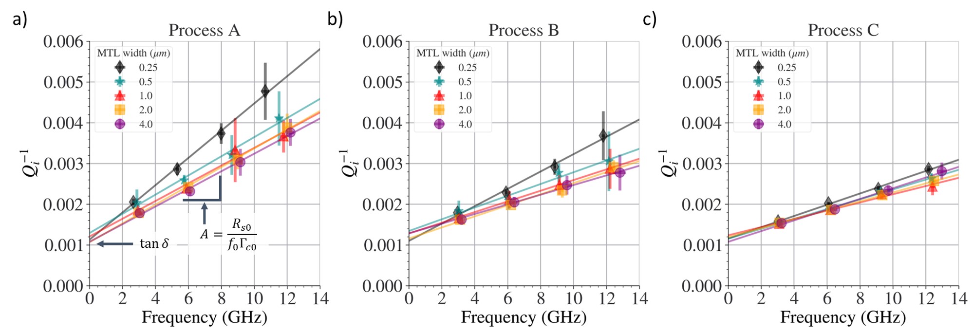
Figure 2 shows obtained from 4 wafers on a total of 22 chips (5 MTL resonators per chip). Each panel of Fig. 2 shows as a function of resonant frequency for all five MTL widths, for particular fabrication process. Each data point and error bar represent the arithmetic mean and 1 standard deviation for a sample of 6-9 chips per process, to statistically describe the loss variation for each respective MTL width for each process. The increased error bars for modes in Processes A and B are due to parasitic ripple in seen in Fig. 1(d). Evaluating a measurement repeatability by re-inserting the same chip several times into a test fixture, yielded maximum spread in the extracted and of and , respectively.
III Data Analysis
To explain the nearly linear dependence of on resonant frequency observed in Fig. 2, a geometric factor concept devised in Appendix A allows to express as
| (4) |
where and are the intrinsic resistances of the ground plane and conducting strip, and are the partial geometric factors associated with resistive loss in the ground plane and conducting strip, is the TEOS-SiO2 dielectric loss tangent, and is the geometric factor associated with loss in the TEOS-SiO2. By making assumptions about the frequency dependence of and , we shall factor out the frequency in Eq. 4.
A frequency dependence for can be written as
| (5) |
where is the intrinsic resistance at a reference frequency that we choose . Although a BCS theory predicts that the scaling exponent decreases from 1.8 to 1.7 over 1–10 GHz for Nb at 4.2 K, the experiments show that the smearing density of states makes up to 10 GHz,[74, 26] which roughly corresponds to the frequency span of our resonators. For an isotropic good superconductor with , the two-fluid model also predicts .[27, 26]
A dielectric loss tangent can be expressed as , where is the material conductivity, and is the vacuum permittivity.[23] According to Jonscher’s universal relaxation law, scales with frequency as , where is the DC conductivity, is the exponential prefactor, and the exponent falls in the range of .[75] Then, at frequencies high enough that , a frequency dependence for can be written as
| (6) |
where is the loss tangent at a reference frequency . Jonscher proposed that low-loss dielectrics with have a nearly “flat loss”, that is , over several decades of frequency.[75] However, can also increase approximately linearly with frequency in some ceramics, glasses and polymers,[35, 76] corresponding to in Eq. 6.
Recalling that per Eq. 18a, application of Eqs. 5 and 6 to Eq. 4 gives
| (7) |
where the quantities with subscript “0” are taken at a reference frequency . Considering for Nb, the linear dependence of with frequency in Fig. 2 suggests in Eq. 7. This implies that for all three processes TEOS-SiO2 has a “flat loss” over at least 3-13 GHz. That result agrees with Tuckerman et al.,[38] who observed similar behavior in a Nb/polyimide transmission line resonator at 4.2 K over 2-20 GHz. However, Kaiser[37] reported for various amorphous thin-film dielectrics at 4.2 K and 0.1-20 GHz, although he ignored the Nb loss in a lumped element resonator.
An embedded MTL like in Fig. 1(b) has . Then, setting and in Eq. 7 leads to the linear form
| (8) |
where represents the MTL net resistive loss, and is the net conductor geometric factor. in the case of the homogeneous MTL. Fitting Eq. 8 to the data sets in Fig. 2 with and being the fitting parameters, the fit slope is proportional to , and the fit y-intercept is .
Figure 2 shows that Process A exhibits larger fit slope , hence higher superconductor loss, for all MTL widths relative to Processes B and C. For MTL width and under, Process B has higher superconductor loss in comparison to Process C, while for the - and --wide MTLs Processes B and C yield similar loss. Furthermore, all MTL widths and processes yield roughly the same y-intercept, corresponding to .
Equation 8 infers that the MTL superconductor loss can be deduced from the fit slope as
| (9) |
For the wide MTL with , the conductor geometric factor can be found from a parallel-plate model[33]
| (10) |
Finding for the narrow MTL with calls for FEM modeling because the parallel-plate approximation accounts for neither the current concentration at the edges of conducting strip[61] nor the field fringing[77] nor the case of irregular geometry of the conducting strip.[78]
Equation 1 infers that a resonator optimized for simultaneous characterization of both superconductor and dielectric losses calls for , which according to Eq. 8 corresponds to a conductor geometric factor . For representative and , one estimates . For the MTL geometry depicted in Fig. 1(b), Eq. 10 predicts at 10 GHz and 4.2 K, which is close to . This makes our MTL resonators sensitive to both types of loss.
IV FEM modeling
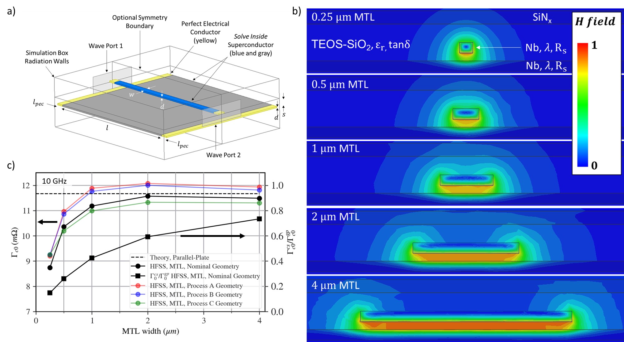
In our work, the conductor geometric factor depends on the field and current distributions inside the wires (see Eqn. 18a). Arguably, Ref. [61] is the only paper solving these for a superconducting strip transmission line, using a proprietary FEM solver. We employ Ansys’ High Frequency Structure Simulator (HFSS)[62] to find geometric factors of the MTL resonators.
HFSS is a full 3D FEM simulator, capable of solving fields, currents, and network parameters for virtually any microwave structure with the ratio of largest to smallest dimension less than . The peculiar aspects of modeling a superconductor network in HFSS are (i) defining the lossy superconductor material by a real conductivity and a negative permittivity; [79] (ii) using perfect electric conductor (PEC) material to connect superconductor members to the ports, since HFSS does not allow superconducting ports;111At the time of this work, the most recent version of HFSS that permits material with complex conductivity and removes a need for PEC ports, was unavailable (iii) enforcing the solve-inside option for the superconductor material, to override the HFSS default setting of only solving inside a material when the conductivity is less than .
IV.1 Defining a superconductor in HFSS
Inserting the superconductor current-field constitutive relationship into Maxwell’s curl-H equation yields
where the parenthesis enclose the superconductor relative permittivity , with being the ordinary dielectric constant associated with displacement current. Modeling a superconductor as a collisionless neutral plasma [79, 81] with Langmuir frequency and dielectric function , comparison of and infers that is the superconductor permittivity in the limit , 222For niobium, is above the superconducting gap frequency and is the London conductivity. Therefore, a lossy superconductor can be defined as a material with real conductivity and real permittivity , applicable over the entire range of temperatures and frequencies of interest. Owing to , a superconductor permittivity is substantially negative quantity. [83]
Generally, the Mattis-Bardin theory allows to tabulate and as HFSS datasets. [21] Here, exploiting the assumption , we define a superconductor in HFSS as a frequency-dependent material. Relating to the experimental intrinsic resistance and penetration depth, a two-fluid model gives that is frequency independent. By the same assumption, modeling as the London conductivity gives . Adapting HFSS to solve inside the superconductor overcomes a limitation of SIBC-based models[50, 51, 52, 53, 54] to an interconnect with a much bigger cross-section than .
IV.2 Modeling a superconducting MTL in HFSS
Figure 3(a) shows 3D HFSS model of a two-port network formed by a superconductor MTL with PEC ports of the same cross-sectional geometry. [21] Note that to determine , we simply model a piece of uniform MTL, not an MTL resonator. To achieve accurate results, the model is electrically short , with being the length of the MTL piece, and the PEC port length is a small fraction of the simulated transmission line . The network analysis driven terminal solution type [62] was used to simulate MTL lengths with PEC port length , at simulation frequency . PEC ports were de-embedded to get only the network parameters pertaining to the superconductor MTL.
All geometries and material definitions were parameterized and the Optimetrics option was used for parameter sweeps. To provide for fast and accurate simulation, the HFSS convergence criteria was set at 0.1-1% for the parameters defined as , , , and .[84] Here, and are the series impedance and shunt admittance of a general transmission line,[85] given by
| (11a) | |||
| (11b) | |||
where and are the elements of the network [Z]-matrix found by HFSS, as described in Appendix B. It is tractable to complete parametric sweeps on the order of 100 simulations in a few hours.
Figure 3(b) shows the magnetic field intensity looking into MTL cross-section, for all five MTL widths, in the case of the nominal geometry and material parameters for Processes B and C. For wide MTL and above, the magnetic field distribution has a parallel-plate-like geometry. For MTL and below, the magnetic field penetrates the majority of the conducting strip, but only a small fraction of the ground plane.
IV.3 Deducing geometric factor from HFSS
Setting the dielectric loss in the HFSS model to zero leads to . The net conductor geometric factor can be found from HFSS simulations, ran at a reference frequency , as
| (12) |
where is the intrinsic microwave resistance corresponding to . Likewise, the partial geometric factor of just the conducting strip can be found by setting the ground plane loss to zero in the above procedure, and vice versa for the ground plane geometric factor. For each MTL geometry, only a single simulation for any resistance value meeting is required, which substantially accelerates the data analysis. We hypothesize that geometric factor can also be computed by numerically integrating Eq. 18a with the fields and currents found by an FEM simulator (see Fig. 3(b)).
The geometric factors found using HFSS were verified to be independent of between 0.1 and . The HFSS results were further validated by comparing the geometric factor by Eq. 12 to the parallel-plate approximation Eq. 10. Figure 3(c) shows that for the MTL with nominal geometry (black solid line) approaches (black dashed line) within 1.5% at MTL width and above. Intuitively, this can be understood from Figure 3(b), where the fringing fields above the conducting strip begin to overlap below a width. Hence, Eq. 10 can be used for preliminary data analysis in wide MTLs with , without resorting to HFSS simulations.
V Results and Discussion
The cross-sectional geometries for each Process and MTL width were measured by focused ion beam (FIB) or scanning transmission electron microscopy (STEM). These actual geometries, including slanted sidewalls of conducting strip, were modeled in HFSS to find the conductor geometric factor using Eq. 12. Finally, such actual geometric factors shown in Fig. 3(c) were utilized to deduce the MTL net intrinsic resistance from the linear fits in Fig. 2 using Eq. 9.
Figure 4 shows the results vs MTL width. The error bars in Fig. 4(a) are obtained by applying the error propagation analysis to Eq. 9, neglecting correlations. The uncertainties in the fit slope and the y-intercept are estimated from the linear regression in Fig. 2. The uncertainty in is found using HFSS to model the effects of MTL geometry variations across the wafer. [84]
Since the ratio decreases with MTL width per Fig. 3(c), the smaller the width, the greater the conducting strip contribution into . In the case of dissimilar , the in Eq. 8 can be written as
| (13) |
where the approximation holds for . For the wide MTL, assuming , the ratio means that the corresponding in Fig. 4(a) is dominated by the strip loss.
Figure 4(a) reveals that for all MTL widths, the Nb loss reduces from Process A to Process B to Process C. Our medium-loss Process B has in the range. This is in agreement with measured by the parallel-plate resonator for Nb thin films at 4.2K, 12 GHz [30] and scaled to 10 GHz using Eq. 5. Our result is also in agreement with the Bardeen–Cooper–Schrieffer (BCS) minimum intrinsic resistance measured by Benvenuti et al. using the RF cavity with thin-film Nb walls at 4.2 K, 1.5 GHz [28] and scaled to 10 GHz, which is shown by the black dashed line in Fig. 4(a). Our low-loss Process C shows that sub-micron Nb interconnects can, remarkably, have below at 4.2 K, which can be attributed to the smearing of density of states.[74] Thus, Processes B and C demonstrate that a CMP planarized Nb interconnect can be scaled into submicron dimensions with no penalty above the minimum theoretical loss.
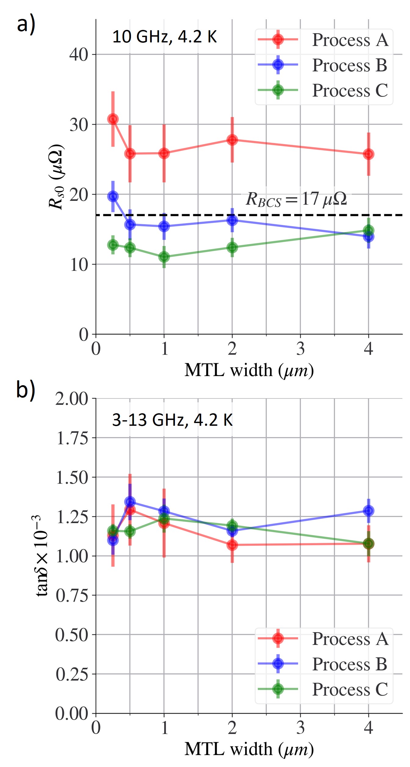
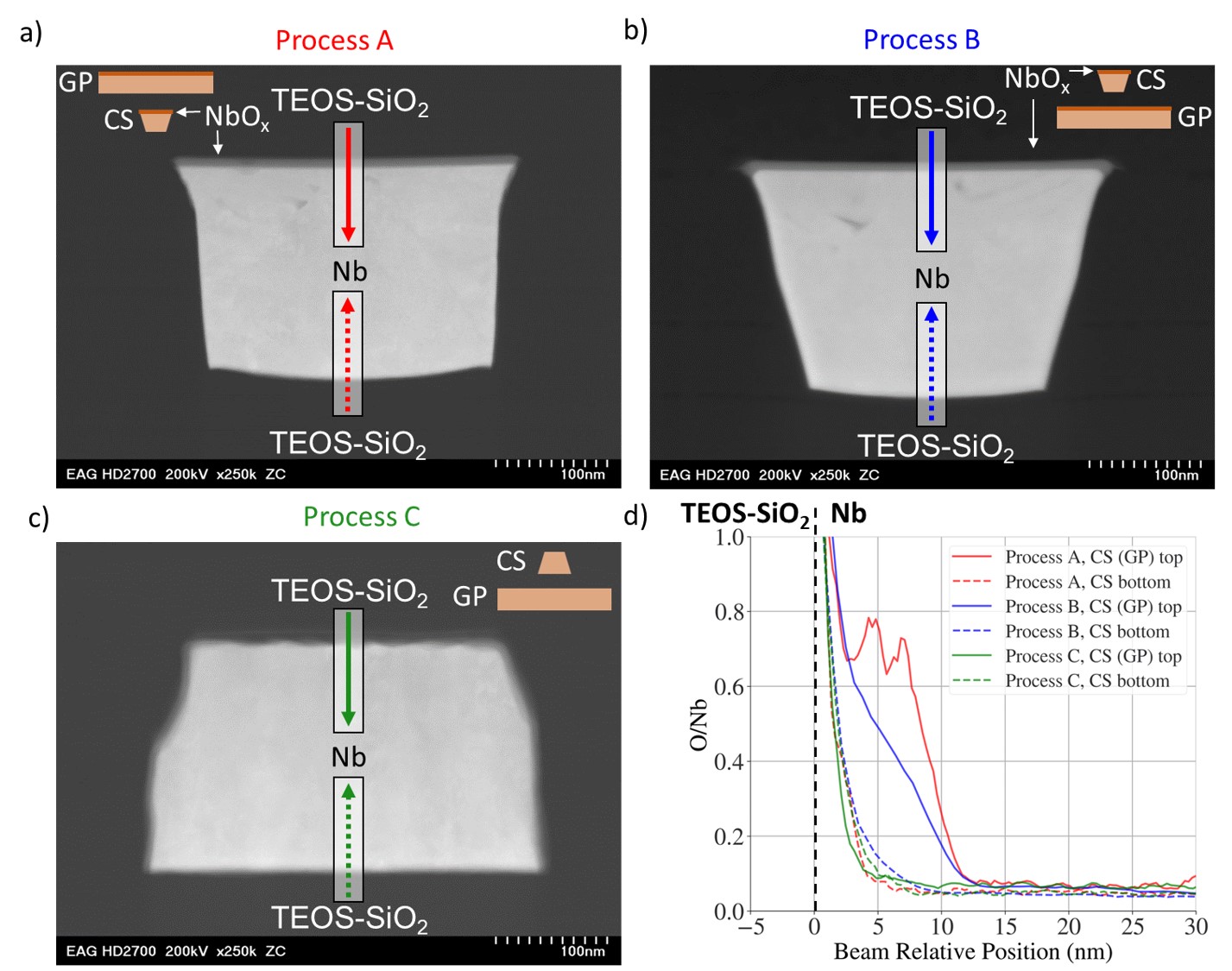
Figure 4(b) shows that all three processes yield approximately the same loss tangent with virtually no MTL width dependence. This is in reasonable agreement with Kaiser, [37] who observed for sputtered amorphous SiO2 at 4.2 K, 1-10 GHz. Therefore, in spite of the same CVD parameters, TEOS-SiO2 is not sensitive to significant differences between the three processes and offers a desirably large processing window.
V.1 variation with process
To explain the Nb loss variation with process seen in Fig. 4(a), we shall rely on a STEM complemented by an energy dispersive X-ray spectroscopy (EDS) with a 0.1-1 nm diameter electron beam and a detection limit of . Figure 5 shows STEM cross-sections of conducting strip looking into the 0.25 wide MTL, for all three processes. The analysis revealed that Processes A and B have 10-nm-thick Nb oxide (NbOx) layer[88] on the top of both the ground plane and conducting strip, resulting from the oxygen plasma treatment to promote the TEOS-SiO2 adhesion. FIB cross-sectioning showed that NbOx has the same thickness in both the ground plane and conducting strip, for all five MTL widths. Process C has no visible NbOx layers.
Figure 5 shows EDS line-cuts for the O/Nb content ratio at the top and bottom TEOS-SiO2/Nb interfaces of a conducting strip, for all three processes. At the time of EDS data collection, it was deemed that only the conducting strip is of interest, so the EDS mapping for the ground plane was not requested. However, using same fabrication recipe for all metal layers in a chip, we suppose that the corresponding top or bottom surfaces of the conducting strip and ground plane have the same O/Nb profile, as conveyed in Fig. 5(d). Comparison of O/Nb profiles between the and conducting strips for Processes A and C suggests that for all three processes the profile is independent of MTL width.
Figure 3(b) shows that for all MTL widths, the RF current concentrates in the ground plane and conducting strip near the TEOS-SiO2/Nb interfaces facing each other. Hence, the MTL resistive loss is mostly sensitive to the oxygen content at such interfaces. For Process A, the oxygen content extends more than 10 nm into the top of the conducting strip, and diminishes within just few nanometers into the bottom of the ground plane. Conversely, for Process B, the oxygen content extends more than 10 nm into the ground plane top, and diminishes within just few nanometers into the conducting strip bottom. At the same time, the conducting strip top in Process A has a higher oxygen concentration than the ground plane top in Process B. Moreover, the inverted microstrip geometry of Process A makes NbOx layer to overlap with the current density peaks at the edges of the conducting strip. [61]
These observations are consistent with about 2x difference in between Processes A and B for all MTL widths.
For Process C, the oxygen content diminishes within just few nanometers into both the ground plane top and the conducting strip bottom. This is consistent with Process C exhibiting 30% lower than Process B for all MTL widths but . We also note that the rough surface of the conducting strip in Process C (see white arrows in Figs. 5(c) and 6(c),(d)) caused by the RIE undercut does not affect the values.
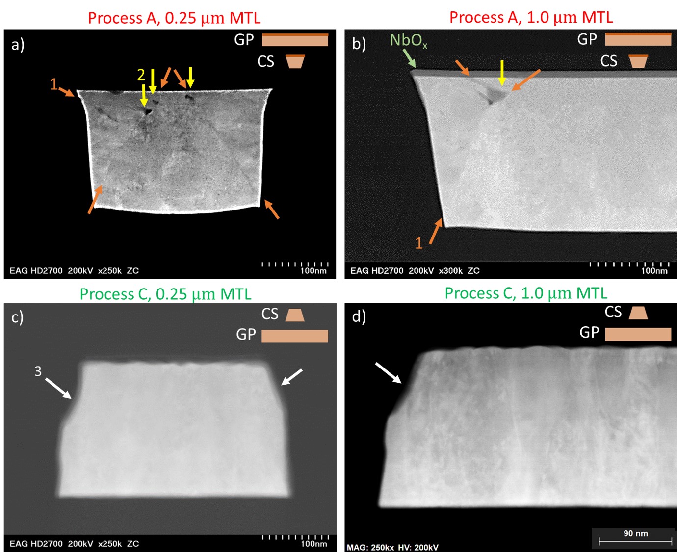
V.2 up-turn at width
Another data trend seen in Fig. 4(a) is the 20-30% up-turn in at 0.25 MTL width for Processes A and B. STEM cross-sections in Fig. 6(a),(b) show that the damascene process entails two Nb growth directions: vertical growth from the trench bottom and horizontal growth from the trench sidewall. [89] The two grain phases, a bottom grain and a sidewall grain, meet at about a 60° angle from the wafer plane. There are two such grain phase boundaries per conducting strip for both Processes A and B, indicated by orange arrows in Fig. 6(a),(b). Conversely, Fig. 6(c),(d) confirms that Process C exhibits only a vertically grown grain.
Aligned with the current flow in conducting strip, the grain phase boundaries may not affect the current distribution. At the same time, morphology of the sidewall grain may reduce the electron mean free path , increasing the BCS resistance , where is the microscopic coherence length in pure Nb. Moreover, Nb voids and vacancies at the grain phase boundaries, indicated by yellow arrows in Fig. 6(a),(b), may reduce and increase . The voids can also act as Nb hydride formation sites,[90] where hydrogen could diffuse into the Nb during fabrication, creating normal-conducting precipitates inside the conducting strip. Subject to proximity effect, hydrides suppress superconductivity in surrounding Nb.
Since the sidewall grain geometry is determined by the trench depth, decreasing MTL width increases both the sidewall grain and void fractions in the conducting strip cross-sectional area. For instance, the sidewall grain fraction increases from about 20% in a 1--wide strip to about 50% in a 0.25--wide strip. According to Fig. 3(c) and Eq. 13, the conducting strip contribution into the net shown in Fig. 4(a) is the largest for a MTL. Therefore, the up-turn for MTL in Processes A and B can be attributed to the sidewall grain phase and/or voids present in conducting strip.
VI Conclusions
To conclude, we have developed a method to disentangle and quantify comparable superconductor and dielectric microwave losses by exploiting their frequency dependence in a multi-mode microstrip transmission line resonator representative of superconducting logic interconnects. The method was used to optimize a planarized process for minimum interconnect loss. With the aid of the geometric factor concept and the 3D superconductor HFSS modeling, the intrinsic resistance was directly compared between different linewidths, stack geometries, and processing conditions. Correlating the Nb resistive loss with the STEM and EDS cross-sectional analysis revealed the mechanisms of loss above the microscopic theoretical minimum, including Nb oxide layer and Nb grain growth orientation.
We demonstrated that Nb interconnects can be scaled down to linewidth with no penalty in microwave loss above the BCS minimum at 4.2 K. Nb sub-micron wires made by planarized Cloisonné process exhibit resistive loss at 4.2 K and 10 GHz, which is even lower than previously reported.[86, 28, 30] We found that dielectric loss tangent for TEOS-derived SiO2 remains unaffected by MTL geometries and processing conditions. This makes it a very attractive interconnect insulator for highly-integrated superconductor circuits, although the dielectric loss is fairly high.
With Nb wires already at or below the theoretical minimum loss, it is worth exploring lower loss dielectrics compatible with the Nb fabrication. The energy efficiency of a ZOR metamaterial clock network relative to the RQL logic at 4.2 K and 10 GHz can be improved from 30% [11] up to 80-90% for Nb with and a dielectric with . Our loss data de-convolution method can be applied to any transmission line resonator including coplanar waveguide and stripline. We hypothesise that by increasing the resonator frequency range and number of modes, while improving the test probe bandwidth, one may unambiguously determine both the superconductor and dielectric loss frequency scaling powers in Eq. 7, by allowing and as the fitting parameters.
Acknowledgements
The authors acknowledge Pavel Borodulin and Edward Kurek for assisting with test fixture design, Andrew Brownfield and David Vermillion for coordinating the test, Justin Goodman and Dr. Steve Sendelbach for assisting with data analysis, Dr. Eric Jones for the assistance with STEM and EDS analysis, Dr. Henry Luo for the penetration depth measurements by SQUID, and Dr. Flavio Griggio for the fruitful discussions. V.V.T. acknowledges insightful discussions with David Gill. S.M.A. acknowledges support from the National Science Foundation through Grant #NSF DMR-2004386, and the U.S. Department of Energy/High Energy Physics through grant #DESC0017931. This research is based on the work supported in part by the ODNI, IARPA, via ARO, contract #W911NF-14-C-0116. The views and conclusions contained herein are those of the authors and should not be interpreted as necessarily representing the official policies or endorsements, either expressed or implied, of the NSF, DOE, ODNI, IARPA, or the US Government. C.A.T.G. acknowledges approval for Public Release NG23-0122. © 2023 Northrop Grumman Systems Corporation
Appendix A Derivation of Eq. 4
Ignoring the radiation loss, the internal Q-factor of a transmission line resonator can be expressed as [23]
| (14) |
where and are the line series resistance and inductance per unit length, and are the line shunt conductance and capacitance per unit length, and is the angular frequency with being the linear frequency. The telegrapher’s equations have for the , , , and of a superconducting transmission line[91, 61, 23]
| (15a) | |||
| (15b) | |||
| (15c) | |||
| (15d) | |||
where the integrals are carried over the line cross-section , and are the line current and voltage, J, H and E are the vector current density, magnetic field and electric field, and are the intrinsic resistance and magnetic penetration depth, and are the vacuum permittivity and permeability, and are the relative dielectric constant and the loss tangent, and it is assumed that in Eqs. 15a and 15b. To provide a simple analytical reference, the approximations on the right of Eqs. 15 hold for a parallel-plate waveguide [30, 33] formed by a dielectric spacer of thickness sandwiched between two superconducting plates of thickness and width , with and being the plate effective surface resistance and effective penetration depth, [59] respectively.
Consider a uniform transmission line formed by conductors, and dielectric layers or tubes. Inserting Eqs. 15 into Eq. 14 yields
| (16) |
Here and are the averaged quantities describing loss in the -th conductor and -th dielectric,
| (17a) | |||
| (17b) | |||
where and are the cross-sectional areas of the -th conductor and -th dielectric. In the case of the homogeneous losses (with arbitrary and distributions), and . Furthermore, in Eq. 16, the partial geometric factors and associated with respective losses in the -th conductor and -th dielectric are
| (18a) | |||
| (18b) | |||
The conductor geometric factor of a superconducting transmission line resonator has units of Ohm, and is defined exclusively by the line cross-sectional geometry and penetration depth . A good superconductor with makes frequency independent, and so the fraction on the right of Eq. 18a. Note that definition 18a involves the field and current density inside the superconducting members. This differs from a cavity geometric factor[26, 36, 29]
| (19) |
which is governed by the ratio of the cavity volume to the walls area and involves magnetic field within that volume only, giving for the cavity Q-factor . Equation 19 is applicable in the case of , where is on the order of the cavity smallest dimension.[92] The concept of a cavity geometric factor is associated with Leontovich’s impedance boundary condition , where and are the respective tangential electric and magnetic fields at the impedance surface, and n is the inward unit vector normal to the surface.[55, 56, 58, 57] The quantity can be seen as a transmission line counterpart of a conductor participation ratio found in voluminous, cavity-like resonators.[39]
The dielectric geometric factor of a transmission line resonator given by Eq. 18b is unitless, and is defined exclusively by the line cross-sectional geometry and . The quantity can be seen as a transmission line counterpart of a dielectric filling factor found in the voluminous resonators[36, 39]
where is the volume of the -th dielectric (), and is the volume of the entire resonator.
An embedded MTL like in Fig. 1(b) calls for and or 3 in Eq. 16, depending on the process. Assuming homogeneous losses within each of the conductor or dielectric members, Eq. 16 gives rise to
| (21a) | |||
| (21b) | |||
where Eqs. 21a and 21b correspond to Process A and Processes B, C, respectively. Furthermore, and are the intrinsic resistances of the ground plane and conducting strip, and are the partial geometric factors associated with resistive loss in respective conductors, , , and are the dielectric loss tangents of the TEOS-SiO2 insulator, Si substrate, SiNx passivation layer and LHe, respectively, and , , and are the partial geometric factors associated with loss in respective materials. Due to [37], and , the Si, SiNx and LHe loss contributions can be ignored in Eqs. 21, both leading to Eq. 4.
Appendix B Derivation of Eqs. 11
Consider a two-port network formed by a transmission line of length . The ABCD (transmission) matrix of such network is [93]
| (22) |
where is the propagation constant, and is the characteristic impedance. For the electrically short network, a quadratic Taylor expansion around yields and . A general transmission line has [85] and , where and are the series impedance and shunt admittance per unit length. Inserting all of the above into Eq. 22 gives
| (23) |
By reciprocity, the elements of the [Z]-matrix corresponding to the ABCD matrix[23] given by Eq. 23 are and . Solving these for the and yields Eqs. 11.
References
- Likharev, Mukhanov, and Semenov [1985] K. Likharev, O. Mukhanov, and V. Semenov, “Resistive single flux quantum logic for the josephson-junction digital technology,” SQUID Journal 85, 1103–1108 (1985).
- Likharev and Semenov [1991] K. K. Likharev and V. K. Semenov, “Rsfq logic/memory family: A new josephson-junction technology for sub-terahertz-clock-frequency digital systems,” IEEE Transactions on Applied Superconductivity 1, 3–28 (1991).
- Hosoya et al. [1991] M. Hosoya, W. Hioe, J. Casas, R. Kamikawai, Y. Harada, Y. Wada, H. Nakane, R. Suda, and E. Goto, “Quantum flux parametron: a single quantum flux device for josephson supercomputer,” IEEE Transactions on Applied Superconductivity 1, 77–89 (1991).
- Herr et al. [2011] Q. P. Herr, A. Y. Herr, O. T. Oberg, and A. G. Ioannidis, “Ultra-low-power superconductor logic,” Journal of applied physics 109, 103903 (2011).
- Volkmann et al. [2012] M. H. Volkmann, A. Sahu, C. J. Fourie, and O. A. Mukhanov, “Implementation of energy efficient single flux quantum digital circuits with sub-aj/bit operation,” Superconductor Science and Technology 26, 015002 (2012).
- Takeuchi et al. [2013] N. Takeuchi, D. Ozawa, Y. Yamanashi, and N. Yoshikawa, “An adiabatic quantum flux parametron as an ultra-low-power logic device,” Superconductor Science and Technology 26, 035010 (2013).
- Peterson and McDonald [1977] R. Peterson and D. McDonald, “Picosecond pulses from josephson junctions: Phenomenological and microscopic analyses,” IEEE Transactions on Magnetics 13, 887–890 (1977).
- Yamanashi et al. [2010] Y. Yamanashi, T. Kainuma, N. Yoshikawa, I. Kataeva, H. Akaike, A. Fijumaki, M. Tnaka, N. Takagi, S. Nagasawa, and M. Hidaka, “100 GHz demonstrations based on the single-flux-quantum cell library for the 10 kA/cm2 nb multi-layer process,” IEICE Transactions on Electronics E93-C, 440–444 (2010).
- Tolpygo [2016] S. K. Tolpygo, “Superconductor digital electronics: Scalability and energy efficiency issues (review article),” Low Temperature Physics 42, 361–379 (2016).
- Chang et al. [2010] L. Chang, D. J. Frank, R. K. Montoye, S. J. Koester, B. L. Ji, P. W. Coteus, R. H. Dennard, and W. Haensch, “Practical strategies for power-efficient computing technologies,” Proceedings of the IEEE 98, 215–236 (2010).
- Strong et al. [2022] J. A. Strong, V. V. Talanov, M. E. Nielsen, A. C. Brownfield, N. Bailey, Q. P. Herr, and A. Y. Herr, “A resonant metamaterial clock distribution network for superconducting logic,” Nature Electronics 5, 171–177 (2022).
- DEVICES and SYSTEMS [2020] I. R. F. DEVICES and SYSTEMS, “Cryogenic electronics and quantum information processing,” (2020).
- Ramzi, Charlebois, and Krantz [2012] A. Ramzi, S. A. Charlebois, and P. Krantz, “Niobium and aluminum josephson junctions fabricated with a damascene cmp process,” Physics Procedia 36, 211–216 (2012).
- Nagasawa et al. [2009] S. Nagasawa, T. Satoh, K. Hinode, Y. Kitagawa, M. Hidaka, H. Akaike, A. Fujimaki, K. Takagi, N. Takagi, and N. Yoshikawa, “New nb multi-layer fabrication process for large-scale sfq circuits,” Physica C: Superconductivity 469, 1578–1584 (2009).
- Kaanta et al. [1987] C. Kaanta, W. Cote, J. Cronin, K. Holland, P.-I. Lee, and T. Wright, “Submicron wiring technology with tungsten and planarization,” in 1987 International Electron Devices Meeting (IEEE, 1987) pp. 209–212.
- Guthrie et al. [1992] W. L. Guthrie, W. J. Patrick, E. Levine, H. C. Jones, E. A. Mehter, T. F. Houghton, G. T. Chiu, and M. A. Fury, “A four-level vlsi bipolar metallization design with chemical-mechanical planarization,” IBM journal of research and development 36, 845–857 (1992).
- Krishnan, Nalaskowski, and Cook [2010] M. Krishnan, J. W. Nalaskowski, and L. M. Cook, “Chemical mechanical planarization: slurry chemistry, materials, and mechanisms,” Chemical reviews 110, 178–204 (2010).
- Egan et al. [2021] J. Egan, M. Nielsen, J. Strong, V. V. Talanov, E. Rudman, B. Song, Q. Herr, and A. Herr, “Synchronous chip-to-chip communication with a multi-chip resonator clock distribution network,” arXiv preprint arXiv:2109.00560 (2021).
- Dai et al. [2022] H. Dai, C. Kegerreis, D. W. Gamage, J. Egan, M. Nielsen, Y. Chen, D. Tuckerman, S. Peek, B. Yelamanchili, M. Hamilton, et al., “Isochronous data link across a superconducting nb flex cable with 5 femtojoules per bit,” Superconductor Science and Technology (2022).
- Kautz [1978] R. L. Kautz, “Picosecond pulses on superconducting striplines,” Journal of Applied Physics 49, 308–314 (1978).
- Talanov et al. [2022] V. V. Talanov, D. Knee, D. Harms, K. Perkins, A. Urbanas, J. Egan, Q. Herr, and A. Herr, “Propagation of picosecond pulses on superconducting transmission line interconnects,” Superconductor Science and Technology 35, 055011 (2022).
- Tzimpragos et al. [2022] G. Tzimpragos, J. Volk, A. Wynn, E. Golden, and T. Sherwood, “Pulsar: A superconducting delay-line memory,” arXiv preprint arXiv:2205.08016 (2022).
- Pozar [2011] D. M. Pozar, Microwave engineering, 4th ed. (John wiley & sons, 2011).
- Fairbank [1949] W. M. Fairbank, “High frequency surface resistivity of tin in the normal and superconducting states,” Physical Review 76, 1106 (1949).
- Maxwell, Marcus, and Slater [1949] E. Maxwell, P. Marcus, and J. C. Slater, “Surface impedance of normal and superconductors at 24,000 megacycles per second,” Physical Review 76, 1332 (1949).
- Turneaure, Halbritter, and Schwettman [1991] J. Turneaure, J. Halbritter, and H. Schwettman, “The surface impedance of superconductors and normal conductors: The mattis-bardeen theory,” Journal of Superconductivity 4, 341–355 (1991).
- Newman and Lyons [1993] N. Newman and W. G. Lyons, “High-temperature superconducting microwave devices: fundamental issues in materials, physics, and engineering,” Journal of Superconductivity 6, 119–160 (1993).
- Benvenuti et al. [1999] C. Benvenuti, S. Calatroni, I. Campisi, P. Darriulat, M. Peck, R. Russo, and A.-M. Valente, “Study of the surface resistance of superconducting niobium films at 1.5 ghz,” Physica C: Superconductivity 316, 153–188 (1999).
- Hein [1999] M. Hein, High-temperature-superconductor thin films at microwave frequencies, Vol. 155 (Springer Science & Business Media, 1999).
- Taber [1990] R. Taber, “A parallel plate resonator technique for microwave loss measurements on superconductors,” Review of scientific instruments 61, 2200–2206 (1990).
- Martens et al. [1991] J. S. Martens, V. M. Hietala, D. S. Ginley, T. E. Zipperian, and G. K. G. Hohenwarter, “Confocal resonators for measuring the surface resistance of high-temperature superconducting films,” Applied Physics Letters 58, 2543–2545 (1991).
- Mazierska [1997] J. Mazierska, “Dielectric resonator as a possible standard for characterization of high temperature superconducting films for microwave applications,” Journal of Superconductivity 10, 73–84 (1997).
- Talanov et al. [2000] V. V. Talanov, L. V. Mercaldo, S. M. Anlage, and J. H. Claassen, “Measurement of the absolute penetration depth and surface resistance of superconductors and normal metals with the variable spacing parallel plate resonator,” Review of Scientific Instruments 71, 2136–2146 (2000).
- Anlage [2021] S. M. Anlage, “Microwave superconductivity,” IEEE Journal of Microwaves 1, 389–402 (2021).
- Zuccaro et al. [1997] C. Zuccaro, M. Winter, N. Klein, and K. Urban, “Microwave absorption in single crystals of lanthanum aluminate,” Journal of Applied Physics 82, 5695–5704 (1997).
- Krupka et al. [1998] J. Krupka, K. Derzakowski, B. Riddle, and J. Baker-Jarvis, “A dielectric resonator for measurements of complex permittivity of low loss dielectric materials as a function of temperature,” Measurement Science and Technology 9, 1751 (1998).
- Kaiser [2011] C. Kaiser, High quality Nb/Al-AlOx/Nb Josephson junctions: technological development and macroscopic quantum experiments, Vol. 4 (KIT Scientific Publishing, 2011).
- Tuckerman et al. [2016] D. B. Tuckerman, M. C. Hamilton, D. J. Reilly, R. Bai, G. A. Hernandez, J. M. Hornibrook, J. A. Sellers, and C. D. Ellis, “Flexible superconducting nb transmission lines on thin film polyimide for quantum computing applications,” Superconductor Science and Technology 29, 084007 (2016).
- McRae et al. [2020] C. R. H. McRae, H. Wang, J. Gao, M. R. Vissers, T. Brecht, A. Dunsworth, D. P. Pappas, and J. Mutus, “Materials loss measurements using superconducting microwave resonators,” Review of Scientific Instruments 91, 091101 (2020).
- Young et al. [1960] D. R. Young, J. C. Swihart, S. Tansal, and N. H. Meyers, “Use of a superconducting transmission line for measuring penetration depths,” Solid-State Electronics 1, 378–380 (1960).
- Mason and Gould [1969] P. V. Mason and R. W. Gould, “Slow-wave structures utilizing superconducting thin-film transmission lines,” Journal of Applied Physics 40, 2039–2051 (1969).
- Henkels and Kircher [1977] W. Henkels and C. Kircher, “Penetration depth measurements on type ii superconducting films,” Magnetics, IEEE Transactions on 13, 63–66 (1977).
- Anlage et al. [1989] S. M. Anlage, H. Sze, H. J. Snortland, S. Tahara, B. Langley, C.-B. Eom, M. Beasley, and R. Taber, “Measurements of the magnetic penetration depth in yba2cu3o7- thin films by the microstrip resonator technique,” Applied physics letters 54, 2710–2712 (1989).
- Langley et al. [1991] B. W. Langley, S. M. Anlage, R. F. W. Pease, and M. R. Beasley, “Magnetic penetration depth measurements of superconducting thin-films by a microstrip resonator technique,” Review of Scientific Instruments 62, 1801–1812 (1991).
- Megrant et al. [2012] A. Megrant, C. Neill, R. Barends, B. Chiaro, Y. Chen, L. Feigl, J. Kelly, E. Lucero, M. Mariantoni, P. J. O’Malley, et al., “Planar superconducting resonators with internal quality factors above one million,” Applied Physics Letters 100, 113510 (2012).
- Khalil et al. [2012] M. S. Khalil, M. Stoutimore, F. Wellstood, and K. Osborn, “An analysis method for asymmetric resonator transmission applied to superconducting devices,” Journal of Applied Physics 111, 054510 (2012).
- Belohoubek and Denlinger [1975] E. Belohoubek and E. Denlinger, “Loss considerations for microstrip resonators (short papers),” IEEE Transactions on Microwave Theory and Techniques 23, 522–526 (1975).
- Oates, Tolpygo, and Bolkhovsky [2017] D. E. Oates, S. K. Tolpygo, and V. Bolkhovsky, “Submicron nb microwave transmission lines and components for single-flux-quantum and analog large-scale superconducting integrated circuits,” IEEE Transactions on Applied Superconductivity 27, 1–5 (2017).
- Krupka et al. [2006] J. Krupka, J. Breeze, A. Centeno, N. Alford, T. Claussen, and L. Jensen, “Measurements of permittivity, dielectric loss tangent, and resistivity of float-zone silicon at microwave frequencies,” IEEE Transactions on microwave theory and techniques 54, 3995–4001 (2006).
- Yassin and Withington [1995] G. Yassin and S. Withington, “Electromagnetic models for superconducting millimetre-wave and sub-millimetre-wave microstrip transmission lines,” Journal of Physics D: Applied Physics 28, 1983–1991 (1995).
- Rafique et al. [2005] M. R. Rafique, I. Kataeva, H. Engseth, M. Tarasov, and A. Kidiyarova-Shevchenko, “Optimization of superconducting microstrip interconnects for rapid single-flux-quantum circuits,” Superconductor Science and Technology 18, 1065–1072 (2005).
- Belitsky et al. [2006] V. Belitsky, C. Risacher, M. Pantaleev, and V. Vassilev, “Superconducting microstrip line model studies at millimetre and sub-millimetre waves,” International journal of infrared and millimeter waves 27, 809–834 (2006).
- U-Yen, Rostem, and Wollack [2018] K. U-Yen, K. Rostem, and E. J. Wollack, “Modeling strategies for superconducting microstrip transmission line structures,” IEEE Transactions on Applied Superconductivity 28, 1–5 (2018).
- Amini and Mallahzadeh [2021] M. H. Amini and A. Mallahzadeh, “Modeling of superconducting components in full-wave simulators,” Journal of Superconductivity and Novel Magnetism 34, 675–681 (2021).
- Leontovich [1944] M. Leontovich, “A new method to solve problems of em wave propagation over the earth surface,” USSR Academy of Sciences Trans., Physics Series 8, 16–22 (1944).
- Leontovich [1948] M. Leontovich, “Approximate boundary conditions for the electromagnetic field on the surface of a good conductor,” Investigations on Radiowave Propagation 2, 5–12 (1948).
- Senior [1960] T. Senior, “Impedance boundary conditions for imperfectly conducting surfaces,” Applied Scientific Research, Section B 8, 418–436 (1960).
- Miller and Talanov [1961] M. A. Miller and V. I. Talanov, “The use of the surface impedance concept in the theory of electromagnetic surface waves,” (in Russian) Izvestia VUZov Radiofizika 4, 795–830 (1961), [Onde superficiali, Springer Berlin Heidelberg, 2011, pp. 257–347].
- Klein et al. [1990] N. Klein, H. Chaloupka, G. Müller, S. Orbach, H. Piel, B. Roas, L. Schultz, U. Klein, and M. Peiniger, “The effective microwave surface impedance of high t c thin films,” Journal of Applied Physics 67, 6940–6945 (1990).
- Mattis and Bardeen [1958] D. C. Mattis and J. Bardeen, “Theory of the anomalous skin effect in normal and superconducting metals,” Physical Review 111, 412 (1958).
- Sheen et al. [1991] D. M. Sheen, S. M. Ali, D. E. Oates, R. S. Withers, and J. Kong, “Current distribution, resistance, and inductance for superconducting strip transmission lines,” IEEE Transactions on Applied Superconductivity 1, 108–115 (1991).
- Release 2021 R2 [2021] Release 2021 R2, HFSS, ANSYS, Canonsburg, PA (2021).
- Swihart [1961] J. C. Swihart, “Field solution for a thin-film superconducting strip transmission line,” Journal of Applied Physics 32, 461–469 (1961).
- Anlage and Wu [1992] S. M. Anlage and D. H. Wu, “Magnetic penetration depth measurements in cuprate superconductors,” Journal of Superconductivity 5, 395–402 (1992).
- Rocha et al. [2004] O. Rocha, C. Viana, L. Gonçalves, and N. Morimoto, “Electrical characteristics of pecvd silicon oxide deposited with low teos contents at low temperatures,” 2004 Microelectronics Technology and Devices SBMICRO , 295–300 (2004).
- Luo [2021] H. Luo, Modelling and Measurement of Reciprocal Quantum Logic Circuits, Ph.D. thesis, University of Maryland College Park (2021).
- Tolpygo et al. [2021] S. K. Tolpygo, E. B. Golden, T. J. Weir, and V. Bolkhovsky, “Inductance of superconductor integrated circuit features with sizes down to 120 nm,” Superconductor Science and Technology 34, 085005 (2021).
- Khanna and Garault [1983] A. Khanna and Y. Garault, “Determination of loaded, unloaded, and external quality factors of a dielectric resonator coupled to a microstrip line,” IEEE Transactions on Microwave Theory and Techniques 31, 261–264 (1983).
- Cote et al. [1995] D. R. Cote, S. Nguyen, W. J. Cote, S. L. Pennington, A. K. Stamper, and D. V. Podlesnik, “Low-temperature chemical vapor deposition processes and dielectrics for microelectronic circuit manufacturing at ibm,” IBM Journal of Research and Development 39, 437–464 (1995).
- Chin et al. [1992] C. C. Chin, D. E. Oates, G. Dresselhaus, and M. S. Dresselhaus, “Nonlinear electrodynamics of superconducting nbn and nb thin films at microwave frequencies,” Phys. Rev. B 45, 4788–4798 (1992).
- Golosovsky, Snortland, and Beasley [1995] M. A. Golosovsky, H. J. Snortland, and M. R. Beasley, “Nonlinear microwave properties of superconducting nb microstrip resonators,” Phys. Rev. B 51, 6462–6469 (1995).
- Jutzi et al. [2003] W. Jutzi, S. Wuensch, E. Crocoll, M. Neuhaus, T. Scherer, T. Weimann, and J. Niemeyer, “Microwave and dc properties of niobium coplanar waveguides with 50-nm linewidth on silicon substrates,” IEEE transactions on applied superconductivity 13, 320–323 (2003).
- Petersan and Anlage [1998] P. J. Petersan and S. M. Anlage, “Measurement of resonant frequency and quality factor of microwave resonators: Comparison of methods,” Journal of Applied Physics 84, 3392–3402 (1998).
- Philipp and Halbritter [1983] A. Philipp and J. Halbritter, “Investigation of the gap edge density of states at oxidized niobium surfaces by rf measurements,” IEEE Transactions on Magnetics 19, 999–1002 (1983).
- Jonscher [1977] A. K. Jonscher, “The ‘universal’ dielectric response,” nature 267, 673–679 (1977).
- Baker-Jarvis et al. [2010] J. Baker-Jarvis, M. D. Janezic, B. Riddle, and S. Kim, “Behavior of () and tan for a class of low-loss materials,” in CPEM 2010 (IEEE, 2010) pp. 289–290.
- Chang [1979] W. Chang, “The inductance of a superconducting strip transmission line,” Journal of Applied Physics 50, 8129–8134 (1979).
- Guo et al. [2020] Y. Guo, D. Kim, J. He, S. Yong, Y. Liu, X. Ye, and J. Fan, “Limitations of first-order surface impedance boundary condition and its effect on 2d simulations for pcb transmission lines,” in 2020 IEEE International Symposium on Electromagnetic Compatibility & Signal/Power Integrity (EMCSI) (IEEE, 2020) pp. 422–427.
- Mei and Liang [1991] K. K. Mei and G.-C. Liang, “Electromagnetics of superconductors,” IEEE transactions on microwave theory and techniques 39, 1545–1552 (1991).
- Note [1] At the time of this work, the most recent version of HFSS that permits material with complex conductivity and removes a need for PEC ports, was unavailable.
- Mishonov [1991] T. M. Mishonov, “Predicted plasma oscillations in the bi2sr2cacu2o8 high-temperature superconductor,” Physical Review B 44, 12033–12034 (1991).
- Note [2] For niobium, is above the superconducting gap frequency.
- Glover III and Tinkham [1957] R. Glover III and M. Tinkham, “Conductivity of superconducting films for photon energies between 0.3 and 40 ,” Physical Review 108, 243 (1957).
- Garcia [2022] C. A. T. Garcia, Materials Characterization for Sub-micron Superconducting Interconnects in Reciprocal Quantum Logic Circuits, Ph.D. thesis, University of Maryland, College Park (2022).
- Ramo, Whinnery, and Van Duzer [1994] S. Ramo, J. R. Whinnery, and T. Van Duzer, Fields and waves in communication electronics (John Wiley & Sons, 1994).
- Group [2012] L. R. Group, SRIMP, Cornell Univ. (2012).
- LABS [2022] LABS, EAG, EAG (2022).
- Halbritter [1987] J. Halbritter, “On the oxidation and on the superconductivity of niobium,” Applied Physics A Solids and Surfaces 43, 1–28 (1987).
- Ju et al. [2002] S.-P. Ju, C.-I. Weng, J.-G. Chang, and C.-C. Hwang, “Molecular dynamics simulation of sputter trench-filling morphology in damascene process,” Journal of Vacuum Science & Technology B: Microelectronics and Nanometer Structures Processing, Measurement, and Phenomena 20, 946–955 (2002).
- Romanenko et al. [2013] A. Romanenko, C. Edwardson, P. Coleman, and P. Simpson, “The effect of vacancies on the microwave surface resistance of niobium revealed by positron annihilation spectroscopy,” Applied Physics Letters 102, 232601 (2013).
- Sass and Stewart [1968] A. Sass and W. Stewart, “Self and mutual inductances of superconducting structures,” Journal of Applied Physics 39, 1956–1963 (1968).
- Vainshtein [1988] L. A. Vainshtein, Electromagnetic waves, 2nd ed. (Moscow, Izdatel’stvo Radio i Sviaz’, In Russian, 1988).
- Paul [2007] C. R. Paul, Analysis of multiconductor transmission lines (John Wiley & Sons, 2007).