]These authors contributed equally.
]These authors contributed equally.
Sharpness of the Berezinskii-Kosterlitz-Thouless transition in disordered NbN films
Abstract
We present a comprehensive investigation of the Berezinskii-Kosterlitz-Thouless (BKT) transition in ultrathin strongly disordered NbN films. Measurements of resistance, current-voltage characteristics and kinetic inductance on the very same device reveal a consistent picture of a sharp unbinding transition of vortex-antivortex pairs that fit standard renormalization group theory without extra assumptions in terms of inhomogeneity. Our experiments demonstrate that the previously observed broadening of the transition is not an intrinsic feature of strongly disordered superconductors and provide a clean starting point for the study of dynamical effects at the BKT transition.
In two dimensions, the superfluid transition is governed by the presence of thermally excited vortex-antivortex pairs [1, 2]. For superfluid 4He films, the defining features of the Berezinskii-Kosterlitz-Thouless (BKT) transition are well understood [3, 4]. In thin-film superconductors an analogous behavior is expected, the transition being caused by dissociation of vortex-antivortex pairs. The transition is manifested as a discontinuous jump in the superfluid phase stiffness at a temperature below the mean-field transition temperature [5, 6]. Moreover, below the voltage-current characteristics are nonlinear, , with a temperature dependent exponent [7]. In the thermodynamic limit, a linear voltage response regime exists above only.
Physics of the BKT-transition is controlled by two energy scales [8]. In order to thermally excite a vortex-antivortex pair in a film, the energy cost for the generation of vortex cores (also called vortex fugacity) as well as the energy scale for the pair dissociation must be sufficiently small. Here and are the coherence length and magnetic penetration depth, respectively. In the dirty limit, both and are proportional to the elastic mean free path. Owing to their small and , ultrathin films of strongly disordered superconductors are the preferred choice for materials that feature a large separation between and the mean field critical temperature .
In the past and were studied for InO and NbN thin films [9, 10, 11] using the two-coil method [12] and standard transport measurements. The two-coil method requires circular films with typical 10 mm diameter, while for dc-transport long strips are needed. Hence, and could not be studied in the same devices limiting the validity of consistency checks. While a qualitative agreement with original theory was observed, measurements of strongly disordered NbN-films always displayed a broadening of the BKT-transition, far stronger than expected for, e.g., finite size effects alone [8, 13]. At present, such broadening is believed to be typical for highly disordered superconducting films that are known to feature emergent granularity [14, 15, 16, 17, 18, 19]. Local variations of the modulus of the order parameter and superfluid stiffness could, in principle, explain the observed smearing of the expected discontinuous jump in . On the other hand, such smearing introduces an additional free parameter that inevitably obscures the quantitative analysis.
Within the generally accepted picture, individual signatures of the BKT transition have been observed [13, 10, 9, 12, 20, 21, 22, 23, 24, 25, 47, 11, 26, 27, 28]. In recent years, however, it turned out that each of these signatures is affected by experimental subtleties that need to be controlled in order to reliably test the level of consistency [29, 30]. The most popular signature, the non-linearity of , is also the most difficult to interpret, as many other effects affect it. For example, any fluctuation induced broadening of the resistive transition leads to non-linear via heating. This can mimic a power-law behavior, in particular close to the normal state resistance and for materials with K [31]. To address this issue, a set of techniques is desirable that do not extrinsically broaden the transition and allows for all types of measurements to be performed on the very same device.
In this Letter, we observe a sharp BKT-transition in strongly disordered NbN films while the resistive transition is smeared over several kelvins. Using a low-frequency resonator technique compatible with four terminal DC-measurements, we unambiguously identify the BKT- and mean field transition temperatures. We find an excellent agreement of both and extracted from DC-resistance and superfluid stiffness in disjunct temperature regimes. The inductively measured stiffness shows excellent agreement with the values extracted from non-linear DC-transport, provided that voltages are sufficiently small. Our results provide a solid basis for the study of more complex non-equilibrium properties of ultra-thin and strongly disordered superconductors.
Our NbN films are grown by atomic layer deposition (ALD - 75 cycles) [32] with a thickness nm on top of a thermally oxidized silicon wafer. Over several months at ambient conditions, the NBN-film gradually oxidizes, signaled by an increase of the sheet resistance. Using standard electron beam lithography and selective etching techniques we prepared long ( 100-200 squares) meander structures of width ranging from 10 - 200 µm with a total kinetic inductance of nH. The samples are mounted into a cold RLC circuit, whose resonance frequency provides access to the sheet kinetic inductance of the sample [33, 34]. The resonance frequency of the circuit varies between 0.5 - 3 MHz, depending on . From the kinetic inductance, the superfluid stiffness is inferred as
| (1) |
where is the Planck’s constant, the electron charge and being Boltzmann’s constant. The parameters of our films are well in line with those of [35, 13], albeit with lower thickness for the same values of and . Additional voltage probes allow for measurement of DC characteristics on the same device. Resistance values were always extracted from the linear regime of .
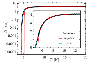
We start by establishing DC transport properties. Figure 1 shows resistance as function of temperature for a typical meander. The transition is strongly broadened by fluctuations of both amplitude and phase fluctuations of the order parameter [36, 37, 38, 39, 40, 34].
Fitting in Fig. 1 for (red line) reveals a mean-field transition temperature K (see [34] for details). Below , phase fluctuations of the order parameter generate resistance, where has the ’square root cusp’ form [5, 7, 36, 37, 38, 39, 34]. Good agreement is found between theory (blue line) and experiment. Very similar results are found also for other devices with different width and length [34].
According to Halperin-Nelson (HN) theory, takes the form [7]
| (2) |
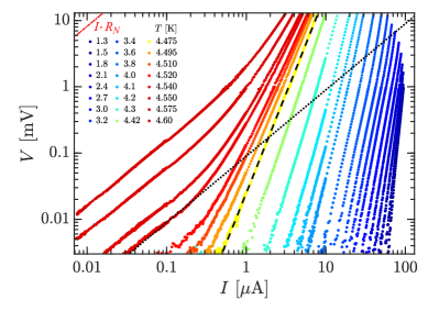
with exponent and prefactor . Hence, power-law behavior of -characteristics below , is another hallmark of the BKT-transition. Increasing temperature decreases and thus . At the universal transition point (dashed in Fig. 2) a characteristic jump to is predicted.
In Figure 2 we present the evolution of with temperature. At low temperatures and voltages the double-logarithmic plot reveals the expected power-law dependence. Above and for sufficiently low current is expected to be linear. The linear regime is limited first by current-induced dissociation of vortex-antivortex pairs, leading again to power-law behavior of , but now with values of smaller than 3. Note that the voltage level is orders of magnitude below (red line in top left corner of Fig. 2).
At higher temperatures and in a wider voltage range turns out to be much more complex [36, 37, 34]. At currents exceeding 10 µA and heating effects start to play a role, rendering the -characteristics very complex and even dependent on the speed of current sweeps [34]. Above the linear part of may be buried in the background noise, mimicking power-law behavior. Both above and below , heating effects can affect the observed power law exponent. Based on -characteristics alone, it is thus very hard to judge whether values for and even are correct when extracted from .
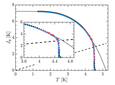
As a consistency check, extracted from is plotted as red dots in Fig. 3 together with (black dots) measured in equilibrium via the kinetic inductance . The excellent agreement between the two independent data sets ensures the was extracted in the right regime and substantiates our analysis of the DC measurements. Very close to the universal transition point at (dashed line), drops to zero within 50 mK. The BKT transition is thus much sharper than in previous experiments on ultrathin NbN films [10, 35, 21]. Also and obtained from () and () match within 1% even though data were obtained in disjunct temperature intervals.
The gradual decrease of towards higher can be described by the BCS expression [10, 13]
| (3) |
(grey line), which accounts for the depletion of by quasiparticle excitations. In order to obtain a good match, it is established practice [10, 13] to use , and as independent fitting parameters [34]. The best fit is obtained for K, and with , . While agrees within 30 mK or with the value obtained from the amplitude fluctuations of the order parameter (Fig. 1), the ratio exceeds the BCS-value of 1.764 as observed earlier [10, 41, 35, 21].
Moreover, is smaller than the dirty limit BCS-prediction , consistent with the conjectured suppression of by phase fluctuations [35]. The ratio k for several of our films with k agrees within a few percent with the BCS-value of k [34]. This indicates that disorder effects in are accounted for by alone, while both and substantially differ from their dirty-limit BCS-expressions. An independent confirmation of the value of is highly desirable. Based on direct measurements of via tunneling spectroscopy, Carbillet et al. proposed an interpretation of the large in terms of an underestimation of [18]. In the latter work, was associated with the onset of the resistance, rather than . Here we can exclude this possibility, as our analysis allows for an unambiguous determination of and .
We theoretically describe the drop of , taking the BCS-fit to as input for the BKT renormalization group (RG) equations [8, 42]. In this way, data is closely reproduced by RG theory (blue line in Fig. 3), assuming a vortex fugacity K, or , similar to values reported, e.g., in Ref. [10]. It is instructive to compare with the loss of condensation energy in the vortex cores with effective radius . We write , where is the thermodynamic critical field, and being the vacuum permeability. From the equation for , we find . Using the expression with being the Ginzburg-Levanyuk number [43], we expect K, which is only 4% smaller than K extracted from Fig. 3.
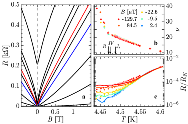
Finally, we investigate signatures of the BKT-transition in magnetic field perpendicular to the film. In the high-field regime and near , is expected to cross over from sublinear to superlinear behavior [44], signaling a transition from amplitude fluctuations of the order parameter to vortex pinning. In Fig. 4a we observe such cross-over at K (blue line) slightly below the range extracted from the other observables. This discrepancy is probably caused by lack of thermal cycling between curves. For the low-field regime, Minnhagen has derived the scaling law [45]
| (4) |
where is the upper critical field and the scaling parameter is a universal function of and . In the Ginzburg-Landau (GL) limit, the coherence length can be written in the form . In Fig. 4b we show separately measured low field data with field cooling procedure. From the measured at fixed value of , the function can be determined from Eq. 4, if is given. Adjusting T leads to a collapse of the set of -curves at low field (Fig. 4b) that corresponds to a coherence length of nm. The error margins mark a deviation from optimal scaling by one dot size. This implies that only weakly depends on . The BKT-transition temperature is reflected as a cusp in which is located within 50 mK of from the -curve (arrows in Fig. 4b).
We use the scaling function in order to predict vs. at very low in Fig 4c. Our directly measured (dots) and data obtained from the scaling expression of Eq. 4 (lines) agree well at the lowest as slightly less at higher .
Discussion: The central result of our work is the observation of a sharp, textbook-like BKT-transition in strongly disordered ultrathin NbN-films. Hence, the previously observed broadening [10, 13] is no genuine consequence of strong (but homogeneous) disorder in superconducting thin films. A possible explanation for the sharpness is a more homogenous distribution of defects in our ALD-deposited films, as opposed to the sputter deposited films in earlier works [41, 17, 18]. Long-range correlated disorder can explain the observed broadening of the transition in terms of a spatial variation of [8, 46, 47]. On the other hand, short-range emergent granularity has been observed in STS for both sputter [17, 48] and ALD [16] deposited films alike. At least at the level of disorder in our films, intrinsic inhomogeneity in the gap distribution appears to be irrelevant at the large length scales that determine the BKT-transition. This finding aligns with previous Monte Carlo simulations conducted on two-dimensional effective XY models [47, 49, 50], which had highlighted that the mere presence of strong quenched disorder does not automatically lead to a broadening of the BKT transition. Instead, it is primarily the strong spatial correlation of the inhomogeneities that causes the smearing of the superfluid-stiffness jump at the critical point.
Most often, the presence of a BKT-transition is deduced from the non-linearity of -characteristics. However, this is not straightforward, as often is strongly affected by heating phenomena. First, power-law behavior can also occur slightly above , where only relatively few vortex-anti-vortex pairs are dissociated. A linear regime exist at the lowest currents only, while already at current densities A/m2 current-induced dissociation dominates over thermal dissociation, leading to power law behavior with that are not considered by standard theory.
These observations are important, because a substantial fraction of the recent literature on ultra-thin materials analyzes -characteristics in the high-power regime above in terms of BKT-behavior (see e.g. [51, 52, 53, 54, 55, 56, 57]). Our work shows that power-law exponents obtained in this regime are unrelated to BKT-physics.
Conclusions: We have shown that ultra-thin superconducting films with strong, but homogeneous, disorder feature a sharp BKT-transition without significant broadening. All relevant observables display quantitatively consistent results, allowing for a precise determination of the BKT- and mean-field transition temperatures as well as other parameters governing the films. Our study lays the ground for future controlled studies of the statics and dynamics of the BKT transition in ultra-thin superconductors when approaching to the superconductor-insulator transition.
Acknowledgements.
We would like to thank M. Ziegler and V. Ripka for NbN film deposition by ALD in the Leibniz IPHT clean room and T. Baturina, E. König, I. Gornyi, A. Mirlin, P. Raychaudhuri, A. Ghosal and F. Evers for helpful comments. The work was financially supported by the European Union’s Horizon 2020 Research and Innovation Program under grant agreements No 862660 QUANTUM E-LEAPS.References
- Kosterlitz and Thouless [1973] J. M. Kosterlitz and D. J. Thouless, Ordering, metastability and phase transitions in two-dimensional systems, J. Phys. C: Solid State Phys. 6, 1181 (1973).
- Kosterlitz [1974] J. M. Kosterlitz, The critical properties of the two-dimensional XY-model, J. Phys. C: Solid State Phys. 7, 1046 (1974).
- Nelson and Kosterlitz [1977] D. R. Nelson and J. M. Kosterlitz, Universal Jump in the Superfluid Density of Two-Dimensional Superfluids, Phys. Rev. Lett. 39, 1201 (1977).
- McQueeney et al. [1984] D. McQueeney, G. Agnolet, and J. D. Reppy, Surface Superfluidity in Dilute 4He-3He Mixtures, Phys. Rev. Lett. 52, 1325 (1984).
- [5] V. Ambegaokar, B. I. Halperin, D. R. Nelson, E. D. Siggia, Dissipation in Two-Dimensional Superfluids, Phys. Rev. Lett. 40, 783 (1978);
- [6] V. Ambegaokar, B. I. Halperin, D. R. Nelson, E. D. Siggia, Dynamics of superfluid films, Phys. Rev. B 21, 1806 (1980).
- Halperin and Nelson [1979] B. I. Halperin and D. R. Nelson, Resistive Transition in Superconducting Films, J. Low Temp. Phys. 36, 599 (1979).
- Benfatto et al. [2009] L. Benfatto, C. Castellani, and T. Giamarchi, Broadening of the Berezinskii-Kosterlitz-Thouless superconducting transition by inhomogeneity and finite-size effects, Phys. Rev. B 80, 214506 (2009).
- A. T. Fiory and Glaberson [1983] A. T. Fiory, A. F. Hebard and W. I. Glaberson, Superconducting phase transitions in indium/indium-oxide thin-film composites, Phys. Rev. B 28, 5075 (1983).
- Yong et al. [2013] J. Yong, T. R. Lemberger, L. Benfatto, K. Ilin, and M. Siegel, Robustness of the Berezinskii-Kosterlitz-Thouless transition in ultrathin NbN films near the superconductor-insulator transition, Phys. Rev. B 87, 184505 (2013).
- Venditti et al. [2019] G. Venditti, J. Biscaras, S. Hurand, N. Bergeal, J. Lesueur, A. Dogra, R. C. Budhani, M. Mondal, J. Jesudasan, P. Raychaudhuri, S. Caprara, and L. Benfatto, Nonlinear characteristics of two-dimensional superconductors: Berezinskii-Kosterlitz-Thouless physics versus inhomogeneity, Phys. Rev. B 100, 064506 (2019).
- Turneaure et al. [2000] S. J. Turneaure, T. R. Lemberger, and J. M. Graybeal, Effect of Thermal Phase Fluctuations on the Superfluid Density of Two-Dimensional Superconducting Films, Phys. Rev. Lett. 84, 987 (2000).
- Mondal et al. [2011a] M. Mondal, S. Kumar, M. Chand, A. Kamlapure, G. Saraswat, G. Seibold, L. Benfatto, and P. Raychaudhuri, Role of the Vortex-Core Energy on the Berezinskii-Kosterlitz-Thouless Transition in Thin Films of NbN, Phys. Rev. Lett. 107, 217003 (2011a).
- Ghosal et al. [1998a] A. Ghosal, M. Randeria, and N. Trivedi, Role of spatial amplitude fluctuations in highly disordered s-wave superconductors, Phys. Rev. Lett. 81, 3940 (1998a).
- Ghosal et al. [2001b] A. Ghosal, M. Randeria, and N. Trivedi, Inhomogeneous pairing in highly disordered s-wave superconductors, Phys. Rev. B 65, 014501 (2001b).
- Sacépé et al. [2008] B. Sacépé, C. Chapelier, T. I. Baturina, V. M. Vinokur, M. R. Baklanov, and M. Sanquer, Disorder-induced inhomogeneities of the superconducting state close to the superconductor-insulator transition, Phys. Rev. Lett. 101, 157006 (2008).
- Carbillet et al. [2016] C. Carbillet, S. Caprara, M. Grilli, C. Brun, T. Cren, F. Debontridder, B. Vignolle, W. Tabis, D. Demaille, L. Largeau, K. Ilin, M. Siegel, D. Roditchev, and B. Leridon, Confinement of superconducting fluctuations due to emergent electronic inhomogeneities, Phys. Rev. B 93, 144509 (2016).
- Carbillet et al. [2020] C. Carbillet, V. Cherkez, M. A. Skvortsov, M. V. Feigel’man, F. Debontridder, L. B. Ioffe, V. S. Stolyarov, K. Ilin, M. Siegel, D. Roditchev, T. Cren, and C. Brun, Spectroscopic evidence for strong correlations between local superconducting gap and local altshuler-aronov density of states suppression in ultrathin nbn films, Phys. Rev. B 102, 024504 (2020).
- Stosiek et al. [2020] M. Stosiek, B. Lang, and F. Evers, Self-consistent-field ensembles of disordered hamiltonians: Efficient solver and application to superconducting films, Phys. Rev. B 101, 144503 (2020).
- Crane et al. [2007] R. W. Crane, N. P. Armitage, A. Johansson, G. Sambandamurthy, D. Shahar, and G. Grüner, Fluctuations, dissipation, and nonuniversal superfluid jumps in two-dimensional superconductors, Phys. Rev. B 75, 094506(R) (2007).
- Mandal et al. [2020] S. Mandal, S. Dutta, S. Basistha, I. Roy, J. Jesudasan, V. Bagwe, L. Benfatto, A. Thamizhavel, and P. Raychaudhuri, Destruction of superconductivity through phase fluctuations in ultrathin -MoGe films, Phys. Rev. B 102, 060501(R) (2020).
- Broun et al. [2007] D. M. Broun, W. A. Huttema, P. J. Turner, S. Özcan, B. Morgan, R. Liang, W. N. Hardy, and D. A. Bonn, Superfluid Density in a Highly Underdoped Superconductor, Phys. Rev. Lett. 99, 237003 (2007).
- Kamal et al. [1994] S. Kamal, D. A. Bonn, N. Goldenfeld, P. J. Hirschfeld, R. Liang, and W. N. Hardy, Penetration Depth Measurements of 3D Critical Behavior in Crystals, Phys. Rev. Lett. 73, 1845 (1994).
- Yong et al. [2012] J. Yong, M. J. Hinton, A. McCray, M. Randeria, M. Naamneh, A. Kanigel, and T. R. Lemberger, Evidence of two-dimensional quantum critical behavior in the superfluid density of extremely underdoped Bi2Sr2CaCu2O8+x, Phys. Rev. B 85, 180507(R) (2012).
- Zuev et al. [2005] Y. Zuev, M. S. Kim, and T. R. Lemberger, Correlation between Superfluid Density and of Underdoped Near the Superconductor-Insulator Transition, Phys. Rev. Lett. 95, 137002 (2005).
- Medvedyeva et al. [2000] K. Medvedyeva, B. J. Kim, and P. Minnhagen, Analysis of current-voltage characteristics of two-dimensional superconductors: Finite-size scaling behavior in the vicinity of the Kosterlitz-Thouless transition, Phys. Rev. B 62, 14531 (2000).
- Ganguly et al. [2015] R. Ganguly, D. Chaudhuri, P. Raychaudhuri, and L. Benfatto, Slowing down of vortex motion at the Berezinskii-Kosterlitz-Thouless transition in ultrathin NbN films, Phys. Rev. B 91, 054514 (2015).
- Mallik et al. [2022] S. Mallik, G. Ménard, G. Saïz, H. Witt, J. Lesueur, A. Gloter, L. Benfatto, M. Bibes, and N. Bergeal, Superfluid stiffness of a KTaO3-based two-dimensional electron gas, arXiv:2204.09094 (2022).
- Tamir et al. [2019] I. Tamir, A. Benyamini, E. J. Telford, F. Gorniaczyk, A. Doron, T. Levinson, D. Wang, F. Gay, B. Sacepe, J. Hone, K. Watanabe, T. Taniguchi, C. R. Dean, A. N. Pasupathy, and D. Shahar, Sensitivity of the superconducting state in thin films, Sci. Advances 5, (2019).
- Benyamini et al. [2019] A. Benyamini, E. J. Telford, D. M. Kennes, D. Wang, A. Williams, K. Watanabe, T. Taniguchi, D. Shahar, J. Hone, C. R. Dean, A. J. Millis, and A. N. Pasupathy, Fragility of the dissipationless state in clean two-dimensional superconductors, Nat. Phys. 15, 947 (2019).
- Levinson et al. [2019] T. Levinson, A. Doron, F. Gorniaczyk, and D. Shahar, Electron-phonon coupling across the superconductor-insulator transition, Phys. Rev. B 100, 184508 (2019).
- Linzen et al. [2017] S. Linzen, M. Ziegler, O. V. Astafiev, M. Schmelz, U. Hübner, M. Diegel, E. Il’ichev, and H.-G. Meyer, Structural and electrical properties of ultrathin niobium nitride films grown by atomic layer deposition, Superconductor Science and Technology 30, 035010 (2017).
- Baumgartner et al. [2021] C. Baumgartner, L. Fuchs, L. Frész, S. Reinhardt, S. Gronin, G. C. Gardner, M. J. Manfra, N. Paradiso, and C. Strunk, Josephson inductance as a probe for highly ballistic semiconductor-superconductor weak links, Phys. Rev. Lett. 126, 037001 (2021).
- [34] See Supplementary Information for further details.
- Mondal et al. [2011b] M. Mondal, A. Kamlapure, M. Chand, G. Saraswat, S. Kumar, J. Jesudasan, L. Benfatto, V. Tripathi, and P. Raychaudhuri, Phase Fluctuations in a Strongly Disordered -Wave NbN Superconductor Close to the Metal-Insulator Transition, Phys. Rev. Lett. 106, 047001 (2011b).
- Baturina et al. [2012] T. I. Baturina, S. V. Postolova, A. Y. Mironov, A. Glatz, M. R. Baklanov, and V. M. Vinokur, Superconducting phase transitions in ultrathin TiN films, Europhys. Lett. 97, 17012 (2012).
- Postolova et al. [2015] S. V. Postolova, A. Y. Mironov, and T. I. Baturina, Nonequilibrium transport near the superconducting transition in TiN films, JETP Letters 100, 635 (2015).
- [38] A.Yu. Mironov, S.V. Postolova, T.I. Baturina, Quantum contributions to the magnetoconductivity of critically disordered superconducting TiN films, J. Physics: Cond. Mat. 40, 485601 (2018)
- [39] K. Kronfeldner, T. I. Baturina, C. Strunk, Multiple crossing points and possible quantum criticality in the magnetoresistance of thin TiN films, Phys. Rev. B 103, 184512 (2021).
- Larkin and Varlamov [2005] A. I. Larkin and A. Varlamov, Theory of Fluctuations in Superconductors (Clarendon Press, Oxford, 2005).
- Semenov et al. [2009] A. Semenov, B. Günther, U. Böttger, H.-W. Hübers, H. Bartolf, A. Engel, A. Schilling, K. Ilin, M. Siegel, R. Schneider, D. Gerthsen, and N. A. Gippius, Optical and transport properties of ultrathin NbN films and nanostructures, Phys. Rev. B 80, 054510 (2009).
- [42] I. Maccari, N. Defenu, L. Benfatto, C. Castellani, T. Enss, Interplay of spin waves and vortices in the two-dimensional XY model at small vortex-core energy, Phys. Rev. B 102, 104505 (2020).
- König et al. [2015] E. J. König, A. Levchenko, I. V. Protopopov, I. V. Gornyi, I. S. Burmistrov, and A. D. Mirlin, Berezinskii-kosterlitz-thouless transition in homogeneously disordered superconducting films, Phys. Rev. B 92, 214503 (2015).
- Garland and Lee [1987] J. C. Garland and H. J. Lee, Influence of a magnetic field on the two-dimensional phase transition in thin-film superconductors, Phys. Rev. B 36, 3638 (1987).
- Minnhagen [1984] P. Minnhagen, Evidence of magnetic field scaling for two-dimensional superconductors, Phys. Rev. B 29, 1440 (1984).
- Benfatto et al. [2013] L. Benfatto, C. Castellani, and T. Giamarchi, Berezinskii–Kosterlitz–Thouless transition within the sine-Gordon approach: The role of the vortex-core energy, 40 Years of Berezinskii–Kosterlitz–Thouless Theory , 161–199 (2013) .
- Maccari et al. [2017] I. Maccari, L. Benfatto, and C. Castellani, Broadening of the Berezinskii-Kosterlitz-Thouless transition by correlated disorder, Phys. Rev. B 96, 060508(R) (2017).
- Kamlapure et al. [2013] A. Kamlapure, T. Das, S. C. Ganguli, J. B. Parmar, S. Bhattacharyya, and P. Raychaudhuri, Emergence of nanoscale inhomogeneity in the superconducting state of a homogeneously disordered conventional superconductor, Scientific Reports 3, 2979 (2013).
- [49] I. Maccari, L. Benfatto, C. Castellani, The BKT Universality Class in the Presence of Correlated Disorder, Condens. Matt. 3, 8 (2018).
- [50] I. Maccari, L. Benfatto, C. Castellani, Disordered XY model: Effective medium theory and beyond, Phys. Rev. B 99, 104509 (2019).
- Reyren et al. [2007] N. Reyren, S. Thiel, A. D. Caviglia, L. F. Kourkoutis, G. Hammerl, C. Richter, C. W. Schneider, T. Kopp, A.-S. Rüetschi, D. Jaccard, M. Gabay, D. A. Muller, J.-M. Triscone, and J. Mannhart, Superconducting interfaces between insulating oxides, Science 317, 1196 (2007) .
- et al. [2014] Z. W.-H. et al., Direct observation of high-temperature superconductivity in one-unit-cell fese films, Chin. Phys. Lett. 31, 017401 (2014).
- Lu et al. [2015] J. M. Lu, O. Zheliuk, I. Leermakers, N. F. Q. Yuan, U. Zeitler, K. T. Law, and J. T. Ye, Evidence for two-dimensional Ising superconductivity in gated MoS2, Science 350, 1353 (2015), .
- Cao et al. [2018] Y. Cao, V. Fatemi, S. Fang, K. Watanabe, T. Taniguchi, E. Kaxiras, and P. Jarillo-Herrero, Unconventional superconductivity in magic-angle graphene superlattices, Nature 556, 43 (2018).
- Park et al. [2021] J. M. Park, Y. Cao, K. Watanabe, T. Taniguchi, and P. Jarillo-Herrero, Tunable strongly coupled superconductivity in magic-angle twisted trilayer graphene, Nature 590, 249 (2021).
- Zhou et al. [2021] H. Zhou, T. Xie, T. Taniguchi, K. Watanabe, and A. F. Young, Superconductivity in rhombohedral trilayer graphene, Nature 598, 434 (2021).
- [57] E. Zhang, Y. M. Xie, Y. Q. Fang, J. L. Zhang, X. Xu, Y. C. Zou, P. L. Leng, X. J. Gao, Y. Zhang, L. F. Ai, Y. D. Zhang, Z. H. Jia, S. S. Liu, J. Y. Yan, W. Zhao, S. Haigh, X. F. Kou, J. S. Yang, F. Q. Huang, K. T. Law, F. X. Xiu, and S. M. Dong, Spin–orbit–parity coupled superconductivity in atomically thin 2M-WS2, Nat. Phys. 19, 106 (2023).
- Lopes dos Santos and Abrahams [1985] J. M. B. Lopes dos Santos and E. Abrahams, Superconducting fluctuation conductivity in a magnetic field in two dimensions, Phys. Rev. B 31, 172 (1985).
- Tinkham [1996] M. Tinkham, Introduction to Superconductivity (McGraw-Hill, 1996).
SUPPLEMENTARY MATERIAL
Sharpness of the Berezinskii-Kosterlitz-Thouless transition in ultrathin NbN films
A. Weitzel et al.
Institut für Experimentelle und Angewandte Physik, University of Regensburg, Regensburg, Germany
I Materials and Methods
We fabricate our samples from ultra-thin NbN films grown by atomic layer deposition (ALD) on top of an amorphous, about 550 nm thick SiO2 layer onto silicon substrate (thermally oxidized silicon wafer with [100] orientation). The growth conditions are completely different for ALD and sputtering. The average growth rate is more than one order of magnitude higher in sputtering. Furthermore, the substrate temperatures are about 300 K higher as well as the kinetic energy of the impinging particles (atoms, ions, electrons). The combination leads to a pronounced growth of NbN crystallites with different orientations linked to each other via grain boundaries [41, 17, 18] In contrast, the layer-by-layer growth of ALD in combination with a low atom mobility on the substrate surface leads to high structural (lateral) homogeneity. Thus, a high density of point defects is accompanied by less pronounced grain boundary formation. A detailed comparison of the structure for ALD-grown and sputtered ultrathin (5 nm) NbN films has not been reported yet and may warrant further study. We believe that such large-scale extrinsic inhomogeneity is much weaker in our ALD-grown films, as compared to epitaxial films.
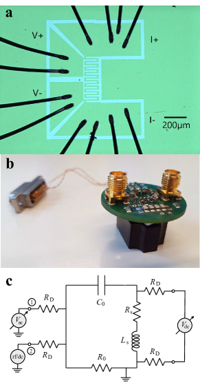
A typical sample chip with a 10 µm wide meander and bond wires is shown in Fig. S1a.
presented in the main text is measured in 4-contact geometry with a standard voltage source (Yokogawa GS 200) and Nanovoltmeter (Agilent 34420A). Each data point corresponds to an characteristic from which the zero bias resistance is inferred by linear fit. The current is swept in a small range from -10 to +10 nA to minimize heating effects. On a Hall bar with thickness nm, width µm and length µm at K at 3.929 Hz we have measured the Hall voltage shown in Fig. S2 and found a sheet resistance of k and a carrier density .

The chip is then integrated into a RLC-circuit mounted at low temperatures (Fig. S1b,c). The meander inductance is obtained from resonance curves measured with a vector network analyzer (VNA, Rohde und Schwarz ZNL3) coupled capacitively to high frequency lines in the cryostat. The input power dBm is chosen such that the quality factor of the circuit remains unchanged upon further reduction. We amplify the output signal at room temperature by 56 dB using a Miteq AU 1447 amplifier. Fast characteristics are measured in 4-contact with a FPGA-base source-measure unit (Nanonis Tramea) with sweep duration of 1-7 s. We measure low voltage regime by using a Femto DLPVA with amplification 80 dB and bandwidth 100 kHz. In parallel, we measure in the high voltage regime without amplification. Low and high regimes overlap over roughly an order of magnitude. All lines are filtered at room temperature by filters with cutoff frequency 100 MHz.
II Circuit Design
The sample chip is placed in a LCC20 chip carrier and is then mounted into a cold RLC circuit. Figure S1b shows a photo of a typical set-up, with green PCB-board as well as brown sample holder beneath. The sample holder is made from Tecasinth (polyimide) and holds an array of pogo pins that establish electric and thermal contact to standard LCC20 chip carriers, and via Al bond wires also to the sample on a Si-chip. To drive and read-out the circuit coaxial cables are needed, which are connected via the SMA-ports on top of the PCB. The other two ports are used to measure the voltage drop over the sample. Fig. S1c shows the corresponding circuit diagram. Four resistors are added to decouple the resonator from the environment, i.e. the lead impedances. For the sample discussed in the main text, a SMD capacitor with capacitance is placed in parallel to the sample with kinetic inductance and resistance , forming the resonator. In the fully superconducting state, a residual resistance m limits the internal quality factor. The lead inductance nH adds to the sample inductance , resulting in a total inductance . In early measurements (Fig. S13) we had placed an additional copper coil in series with the sample adding a typical inductance of 300 nH and a resistance of 50 m.
Using the transmission matrix formalism, the element of the transmission matrix between terminal 1 and 2 (Fig. S1) can be calculated:
| (S.5) |
Therefore, the measured signal can be described by
| (S.6) |
where is the voltage at the input of the network analyzer, is the frequency, is a scaling parameter containing the drive level, is the quality factor, with being decoupling resistors that separate the circuit from lead impedances and is the impedance of the cables. Changes of resonance frequency can be directly connected to changes of the sample’s kinetic inductance.
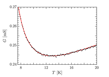
III Circuit Calibration
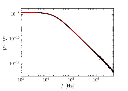
We determine , the capacitance, by heating the circuit with sample to a temperature above , such that the resistance of the sample is very large ( M) when compared to . In this regime, the circuit can be effectively modeled as a low-pass filter, with transfer matrix element:
| (S.7) |
Figure S3 shows measured together with the best fit according to Eq. S.7, giving nF, close to the nominal value of the capacitors ( nF).
For resonators with an additional inductor in series with the sample, we determine its inductance by replacing the sample with a straight bond wire of negligible resistance (50 m) and inductance ( nH). From the resulting resonance frequency , we determine
| (S.8) |
and find typical values around 220 nH.
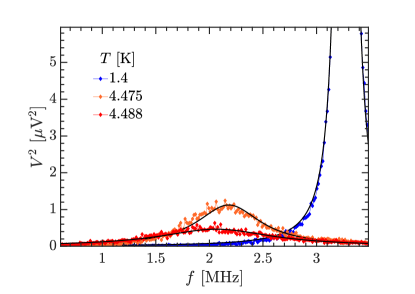
IV Exemplary Spectra
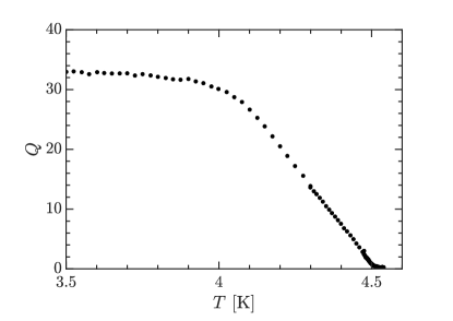
We present some exemplary spectra in Fig. S4. At K a resonance is still clearly resolvable, albeit with a strongly suppressed factor compared to low temperatures. close to is shown Fig. S5. About 0.5 K below , decreases rather linearly towards . A possible explanation for the decrease is that the oscillatory motion of the increasing number of thermally excited, but still bound, vortex-antivortex pairs around their equilibrium distance gives rise to an additional dissipation channel.
V Quality Factor
The quality factor of a resonance curve is defined as the ratio of resonance frequency over the full width at half maximum (FWHM). For the circuit displayed in Fig. S1, can be written as the combination of the circuit’s internal and external quality factors and :
| (S.9) |
where
| (S.10) |
If as well as and are known, small sample resistances can be determined from the internal quality factor.
VI Magnetic Field Compensation
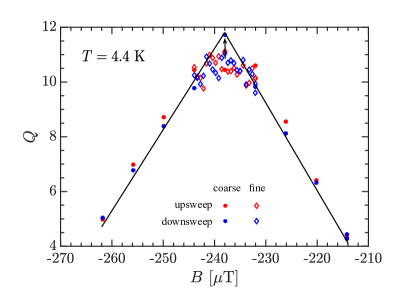
By optimization of the quality factor , the perpendicular magnetic field can be compensated down to a few µT. In Fig. S6 shows a sharp maximum with a width of µT. The precise location of the maximum is obtained from the linear extrapolation of from both sides of the maximum. Negligible hysteresis was observed for up- and down-sweeps. For the experiments presented in the main text, we chose µT to compensate residual fields, indicated by an arrow in Fig. S6. Experience shows that after heating the solenoid above strongly improves the stability of the residual field such that compensation is reliable over several days. All experiments in zero field presented in the main text were performed within six days after field compensation.
VII Fluctuation Contributions to
Our fit of the intrinsically broadened -curve consists of several contributions (see [40, 36, 37] and the references therein):
| (S.11) |
Besides the normal-state resistance , the Aslamazov-Larkin (AL) contribution describes the fluctuation of Cooper pairs above
| (S.12) |
Fluctuating Cooper pairs also affect the diffusion coefficient of unpaired electrons due to the interaction with the Cooper pairs. This included as , named after Maki and Thompson
| (S.13) |
where is the conductance quantum, while the Larkin function and the Maki-Thompson pair breaking parameter are given by
| (S.14) | ||||
| (S.15) |
where the approximate form of in Eqn. S.15 is valid in the limit [58]. Finally, the normal state weak localization and interaction corrections are responsible for the resistance maximum above and read:
| (S.16) |
Four parameters are determined from a curve fit according to Eq. S.11: , , and . The Drude-scattering time enters only logarithmically and is tied to the Drude resistance via Eqs. S.17 below. These parameters are mainly determined by different features of the curve in Fig. S7 : by the sharp rise in the low -region, by the slope above the minimum, by the curvature around the minimum and by the value of at the minimum. Nevertheless, three of the parameters () show some mutual dependency which limits their accuracy to .
The combined strength of is measured by the prefactor . For the pair-breaking parameter we find . Due to the divergence of the fluctuation term at the mean field transition temperature, can be determined more accurately to . From the four parameter fit, we find k. Using the expressions
| (S.17) |
from the free electron model we estimate , a Drude mean free path nm, and an elastic scattering time s. Taking the free electron mass, leads to m/s and a diffusion constant of m2/s, in good agreement with the independent estimate of Eq. S.19.
VIII Dirty limit BCS-fit to
We fit data using
| (S.18) |
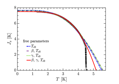
where . Here, and are freely adjustable parameters, is the dirty-limit BCS-expression [59] for , , and being the normal state resistance determined at the maximum in near 12 K. As in Refs. [10, 13], we need three free parameters, , , and , to achieve a good fit. Since also affects the shape of the curve via argument of in Eq. S.18, independent variation and is needed to reproduce the data (purple curve). This becomes evident from fits with one and two free parameters in Fig. S8. The one-parameter (red) and two-parameter (blue and green) fits fail to reproduce the curvature of as well as the absolute values of and the independently measured value of .
IX High-Field Magnetoresistance
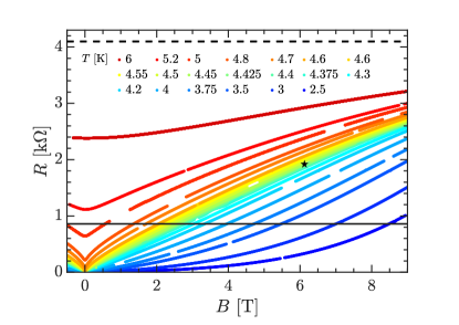
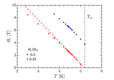
Figure S9 shows magnetoresistance isotherms measured in a Nb3Sn solenoid up to 9 T. Determination of is difficult because the jump in is smeared out over a field range of more than 10 T. As criterion for , we defined a threshold resistance (solid horizontal line in S9) such that extrapolates to (red dots). Note that the value of extracted from the scaling of the low-field magnetoresistance in Fig. 4 corresponds to a resistance of and is thus much closer to the standard criterion . The latter criterion, however, fails close to because the corresponding curve (blue dots) extratolates to much to high temperatures. From we estimate via
| (S.19) |
with nm. Using we find a diffusion constant of cm2/s in good agreement with the independent estimate of Eq. S.17.
X -Characteristics
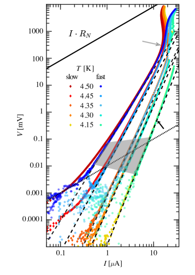
As discussed in the main text, the superfluid stiffness can also be extracted from the power-law exponent of the characteristics using Halperin-Nelson theory [7] (Figs. 2 and 3). Fig. S11 shows typical characteristics in a very narrow temperature regime . In this regime, we employed two different measurement schemes to evaluate the importance of heating effects: Blue curves are fast sweeps of duration 1-7 s, to minimize heating and measurement time. Measurements shown in Fig. 3 in the main text were performed in the fast scheme. We determine power-law exponents from fast sweeps (red dots in Fig. 3) in the main text (Fig. 3) by fitting the data in a region indicated by the shaded grey area to a power law with exponent . Red curves are slow sweeps (duration: 10 minutes) using a nanovoltmeter.
We emphasize the importance of extracting power-law exponents at the lowest possible power regime (, ), to minimize effects of electron heating, which can alter the shape of the -curve. For both the fast and slow measurement scheme, such effects appear in Fig. S11 already at power levels of a few picowatts, where data start to deviate from power-law behavior (black arrow), which we attribute to electron overheating [31]. At much higher power W (grey arrow) we observe a clear divergence of the slowly measured curves (red) from the fast measured curves (blue). Analysis of data in both electron- and chip-heating regimes will likely result in erroneous values of . Heating effects that push the film towards the normal state can be approximated by power law -characteristics in limited -intervals. A typical signature of such analysis is a wide temperature range in which . This width, however, should be much smaller than the total width of the fluctuation regime between and the temperatures where approaches . As indicated by the grey shaded area in Fig. S11), the range of that is governed by the current-induced vortex-anti-vortex depairing is rather small
Above 1 mV, corresponding to power levels of 10 pW/square in our devices, -gradually starts to bend upward because of electron heating. In a limited voltage range also these -characteristics can mimick power-law behavior, leading to an apparently broadened transition. At even higher voltage levels mV, or power levels µW in the whole meander, heating of the sample stage becomes noticable. This leads to heating instabilities and back-bending of the -characteristics.
Slightly below we observe ohmic tails in the slow measurement at low voltage V (red and dark red curve in S11), that are not discernible in the fast sweeps. As pointed out in [29, 30], these tails can result from current noise due to insufficient filtering even at 4He-temperatures. In our set-up, we use -filters with cutoff frequency 100 MHz for all measurement leads. For the slow measurement rounding towards ohmic behavior occurs at slightly higher voltages when compared to the fast measurement. A clarification of this effect requires further study.
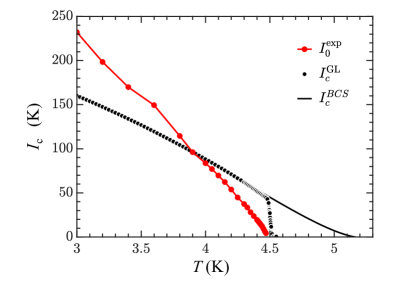
XI Characteristic Currents
Another interesting comparison can be performed between the Ginzburg-Landau (GL) critical current and the Halperin-Nelson (HN) scaling current entering the prefactor in Eq. 2. Withing the error margins of and we can estimate via
| (S.20) |
The error margin is mainly set by the uncertainty of , which is hard to determine reliably from the broad magnetoresistance curves. The scaling current is extracted from the independent measurement of . On the other hand, the full expression for the -characteristics within HN theory reads [7]:
| (S.21) |
with the exponent . From this equation we infer the HN scaling current as:
| (S.22) |
where and are fit parameters in the fit of double-logarithmic , see also Eq. 2 in the main text.
In order to slightly generalize Eq. S.23 we replace by and use the relation (Eq. 1), we find that an expression for that reads identical to the GL-critical current (Eq. S.20), the only difference being that can now be taken form the measurement of rather than assuming the standard GL-form in Eq. S.20.
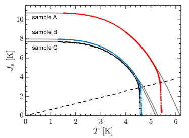
XII Other Devices
We have performed measurements of on several similar devices made from the same wafer over a period of one year. All devices show a sharp jump of near their intersection with the BKT universal line. They differ in width, while the number of squares was kept close to 100, except for the 10 µm wide device, where if was 200. The variations between the films result from different oxidation states. Over the course of several months the films gradually increase in normal state resistance. Table 1 summarizes the relevant sample parameters.
| sample | width [µm] | [k] | [K] | [K] | [k] | ||
|---|---|---|---|---|---|---|---|
| A | 10 | 10.726 | 3.115 | 6.167 | 5.369 | 2.269 | 5.418 |
| B | 10 | 7.981 | 3.964 | 5.276 | 4.601 | 2.496 | 5.988 |
| C | 200 | 7.700 | 5.183 | 4.529 | 2.727 | 6.190 | |
| main text | 10 | 7.511 | 4.093 | 5.175 | 4.488 | 2.521 | 5.940 |