Self-assembly of atomic-scale photonic cavities
Despite tremendous progress in the research on self-assembled nanotechnological building blocks such as macromolecules 1, nanowires 2, and two-dimensional materials 3, synthetic self-assembly methods bridging nanoscopic to macroscopic dimensions
remain unscalable and inferior to biological self-assembly.
In contrast, planar semiconductor technology has had an immense technological impact owing to its inherent scalability, yet it appears unable to reach the atomic dimensions enabled by self-assembly.
Here we use surface forces including Casimir-van der Waals interactions 4 to deterministically self-assemble and self-align suspended silicon nanostructures with void features well below the length scales possible with conventional lithography and etching 5, 6, despite using nothing more than conventional lithography and etching. The method is remarkably robust and the threshold for self-assembly depends monotonically on all governing parameters across thousands of measured devices.
We illustrate the potential of these concepts by fabricating nanostructures, which are impossible to make with any other known method: Waveguide-coupled high- silicon photonic cavities 7, 8 that confine telecom photons to 2 nm air gaps with an aspect ratio of 100, corresponding to mode volumes more than 100 times below the diffraction limit.
Scanning transmission electron microscopy measurements confirm the ability to build devices even with subnanometer dimensions. Our work constitutes the first steps towards a new generation of fabrication technology that combines the atomic dimensions enabled by self-assembly with the scalability of planar semiconductors.
The fabrication of functional materials and devices at the micro- and nanoscale typically follows either a top-down approach, which uses complex sequences of planar technology such as lithography and etching, or a bottom-up approach, where structures are self-assembled using various effects, such as van der Waals, electrostatic, capillary, or hydrogen-bonding forces 9, 10, 11. While top-down nanofabrication underpins the unique scalability of semiconductor technology, the bottom-up approach has enabled a wide range of research on devices with near-atomic dimensions. Such miniaturization is crucial for a wealth of research and technology that rely on an increased surface-to-volume ratio, strong field gradients, or quantum effects. Examples include ultrahigh-frequency surface-acoustic-wave resonators 12, superconducting nanowire single-photon detectors 13, X-ray zone plates 14, and nanopore sequencing of DNA strands 15. In addition, the vision of complex and often hybrid and hetero-integrated devices relying on technology at the few-nanometer scale, sometimes denoted More than Moore, is now central to a wide range of research ranging from biosensing 16 to quantum technologies 17. However, the miniaturization of semiconductor technology has slowed to the point where the so-called technology nodes no longer indicate physical dimensions. For example, the current industry roadmap 6 forecasts no lateral lithography features (minimum half-pitch or physical gate length) below 8 nm for the next 15 years. However, state-of-the-art today is already denoted the “3 nm node” 18. At the same time, while bottom-up approaches can achieve feature sizes down to atomic scales, synthetic self-assembly remains far from capable of replicating the hierarchical and scalable self-assembly in biological systems 11, 19, 20. A practical consequence is that a wealth of research on bottom-up nanotechnology for information technology always had to rely on top-down technology for the interconnect architecture, e.g., lithographically defined wires or waveguides are needed to contact single-molecule devices 21, 22 or single-quantum-dot devices 8. Combining the scalability of top-down planar technology with the resolution of bottom-up approaches would open vast perspectives for both research and technology 9, but they are commonly considered disjoint. Strategies for combining them are scarce 23, 24 and a pathway for their direct integration was so far missing.
Recent developments have brought miniaturization to the center stage also in photonics. Increasing the strength of the interaction between light and matter has been a central goal in quantum optics and photonics for decades and traditionally followed either of two paths: dielectric nanocavities offering high quality factors and scalable waveguide integration but limited confinement or, alternatively, metal nanocavities offering strong spatial confinement due to plasmonic effects 25, 16, 26 but suffering from absorption and limited quality factors. The two approaches can be combined in a hybrid cavity-antenna system 27, but plasmon resonances limit their applicability to visible and short infrared wavelengths. Using dielectric bowtie cavities, it is possible to combine strong spatial confinement with high quality factors at telecom wavelengths, which was predicted in 2005 28 but demonstrated only very recently 5, in part because realistic designs were missing and in part because experimental progress was impeded by the extreme requirements posed on the nanofabrication. Dielectric bowtie cavities harness the field discontinuities at material boundaries to strongly confine light inside dielectrics 29, and hold the promise of unprecedented light-matter interaction strengths, fostering new developments in nanolasers and optical interconnects 30, 31, nonlinear photonics 32, all-optical switching 33, cavity quantum electrodynamics 8, and cavity optomechanics 34. In addition, dielectric bowtie cavities may also enable probing fundamental limits to the light-matter interaction strength 35, 36 as well as investigating the validity of the continuum model of electromagnetism, which is known to break down in plasmonics 37 but has only recently been explored in dielectrics 38. Since the width of the bowtie determines the electromagnetic field enhancement 29, this has put progress in planar semiconductor nanofabrication at the forefront of research in nanophotonics. The first experiment 5 demonstrating confinement of light below the diffraction limit in dielectric bowtie cavities employed 8 nm wide silicon bridges with an aspect ratio of 30 and although minor improvements along this route may be possible, it appears futile to try to scale conventional lithography and etching to atomic dimensions with aspect ratios exceeding 100. Void or low-refractive-index features with extreme aspect ratios are especially challenging to fabricate, but they are required for some of the most radical applications of nanocavities, such as bulk nonlinearities operating at the single-photon level 32 and single-photon emitters for quantum photonic integrated circuits 39.
Here we propose and demonstrate a novel approach to the manufacturing of semiconductor devices with unprecedented dimensions, namely using the ubiquitous surface forces that act on objects separated by a few tens of nanometers, i.e., the van der Waals force and the Casimir force 4. The two are different limits of the same force that arises due to the fluctuations of the quantum vacuum 4 and are normally considered nuisances that cause device failure of micro- and nanomechanical devices 40. In contrast, our experiments aim to harness these forces to enable controlled, deterministic, and directional collapses to fabricate nanostructures with atomic-scale dimensions.
Deterministic self-assembly by surface forces
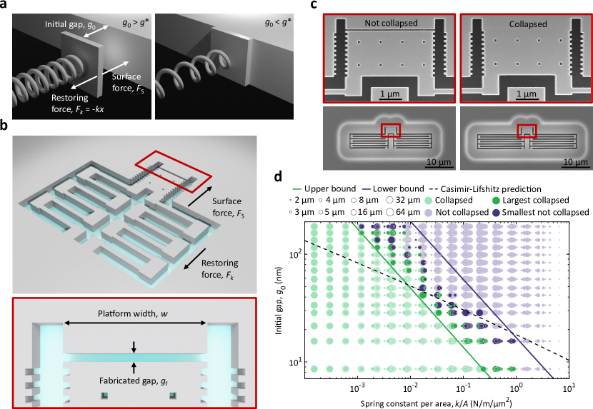
Self-assembly is possible when components are free to move and can adhere to each other, which is often realized in liquid environments 41, but our method takes place in a gas or vacuum. To prevent the components from falling onto the substrate due to gravitational forces while still being free to move, we suspend and attach the components to the surrounding frame by springs, which are etched out of silicon. Common to the surface forces are their power-law dependence on the gap between objects, , leading to pull-in instabilities as illustrated in Fig. 1a: When the nonlinear attractive surface force, , overwhelms the opposing linear restoring force, , at a critical gap 42, , the pull-in instability occurs. The suspended components collapse deterministically and subsequently adhere to each other by van der Waals forces, resulting in a structurally stable self-assembled device.
Although the surface forces are well understood theoretically 4, 43, their exact numerical values are difficult to determine because they depend strongly on parameters such as surface treatment, doping level, and fabrication imperfections 44. Therefore, the starting point of our investigation is to map the surface-force instability as a function of geometry, thus providing design rules for self-assembly by directed collapses. This experiment is implemented in a silicon-on-insulator platform as illustrated in Fig. 1b, using suspended silicon platforms in close proximity to a rigid and anchored silicon structure. The platforms are attached to the frame by two symmetric folded cantilever springs of spring constant , separated from the anchored part by a gap, . Our devices are defined using electron-beam lithography and reactive-ion etching. Subsequently, the platforms are released from the substrate by selective underetching of the oxide layer using anhydrous vapor-phase hydrofluoric acid. The released platforms will collapse or not collapse in-plane onto the anchored structure depending on whether the initial gap, , is larger than the critical gap, , which in turn depends on and . This is illustrated in Fig. 1c, which shows representative scanning electron microscope (SEM) images of two devices with the same and , but different . The stiffer spring provides enough restoring force for the platform to reach a stable equilibrium at a small displacement without collapsing, while that with a smaller spring constant does not, leading to a deterministic and directed collapse.
To map out the set of geometries that lead to directed in-plane collapses, we fabricate 2688 devices distributed across two samples (Sample A: 1536 devices; Sample B: 1152 devices) with varying values of , , and and here we discuss only Sample A (see Methods for details on parameters and data for Sample B, which reproduce the results from Sample A). Note that differs from the initial gap, , because of a 19.4 nm displacement due to the release of the built-in compressive thermal stress after underetching, i.e., nm (see Supplementary Section S1.1 and S1.2 for details). We perform systematic SEM characterization of all devices after underetching and record which structures collapse and which do not. The resulting data is shown in Fig. 1d. For fixed values of and , we identify two gaps: the largest value of for which the collapse occurs and the smallest value of for which the collapse does not occur. Using those gaps, we find that all platforms for which collapse and all platforms for which do not collapse. Given the significant sample size and yield of the experiment, i.e., only 11 devices out of 2688 devices failed due to out-of-plane collapse and/or lithographic errors, these thresholds provide the essential design rules for realizing suspended silicon devices with high-aspect-ratio gaps that avoid unintended pull-in instabilities, such as nano-opto-electromechanical systems 45, or, in the opposite limit, the criterion for deterministic self-assembly.
We include in Fig. 1d the critical gap calculated with the Lifshitz theory of the Casimir-van der Waals force in the proximity force approximation (PFA) for two silicon slabs (see Supplementary Section S1.3). We observe good agreement with the measured collapse threshold in the range where the PFA is expected to be valid, i.e., for gaps in the range of 20 to 50 nm. The model deviates from our experiment for small gaps, but systematic errors in SEM measurements of few-nanometer features can be very significant. The platforms are found to be more prone to collapse than predicted by the model for larger initial gaps and smaller spring constants, which indicates additional attractive contributions to the net surface force, such as electrostatic surface effects 46 and effects beyond the PFA 47, which are both expected to be more important for large gaps. In any case, our static collapse experiment does not aim to replicate the abundance of accurate dynamical measurements of the Casimir force available in the literature 4, 48, 43, 42, 40, but rather to map out the phase space separating collapse from non-collapse in a practical setting relevant for self-assembly. We note that the largest initial gap leading to collapse and the smallest gap not leading to collapse are adjacent data points across our entire data set of 2688 devices, which evidences a robust and reproducible method (see Supplementary Information Section 1.2 for the full data set and further discussions).
Self-assembly of atomic-scale bowtie cavities
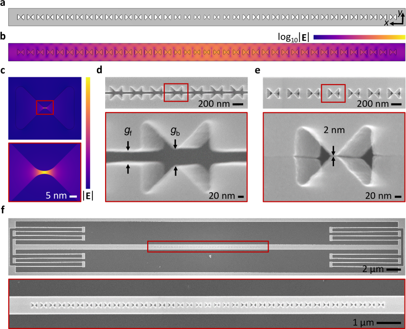
To illustrate the application of our method, we now turn to the realization of photonic nanocavities that confine light in air gaps in a 220 nm thick silicon membrane with aspect ratios exceeding 100. Figure 2a shows the geometry of a nanobeam cavity featuring a unit cell that includes a 2 nm air bowtie and is designed following well-known methods for nanobeam cavities (see Supplementary Section S2 for details on the cavity design). The normalized electric field of the fundamental optical mode is plotted respectively on a log-scale in Fig. 2b and on a linear scale, zooming-in on the central bowtie, in Fig. 2c. The fundamental cavity mode features a resonance wavelength of nm, a quality factor of , and a mode volume of , calculated at the center of the central bowtie 29. Note that the cavity design takes the constraints of our nanofabrication process into account(see Ref. 5 and Supplementary Section S2), except for the use of a 2 nm air void at the bowtie centers, which is well below the resolution of current lithography technology and is therefore instead realized following the design rules provided by Fig. 1d.
The nanobeam cavity is fabricated as two halves, each suspended by two folded cantilevers with a total spring constant of 0.038 N/m. The two halves are separated by a gap, = 50 nm, such that the set {,,} lies deep within the parameter space leading to surface-force-assisted collapses (see Fig. 1d) and therefore the two halves adhere after underetching. Importantly, while the resolution of the nanofabrication limits the absolute value of , the tip-to-tip distance before self-assembly, , and thus the bowtie width in the final device, , are limited only by surface roughness, enabling the realization of atomic-scale air bowties. We fabricate nanocavities with different bowtie widths by varying the offset, , between and in the lithographic mask (see Supplementary Section S3.1 for details on the bowtie unit cell geometry). Figures 2d and e show two halves of a nanobeam cavity and their central bowtie unit cell before and after underetching, resulting in a bowtie width of approximately 2 nm for offset = 10 nm. Figure 2f shows a characteristic device, which includes 22 µm of unpatterned half-beams on each side of the photonic-crystal cavity to increase the surface forces and aid the self-assembly, as well as the two pairs of folded cantilever springs.
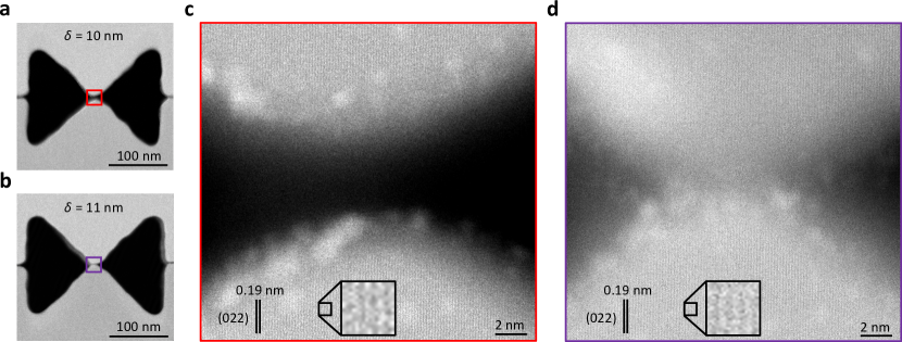
A systematic SEM study of devices with varying offset confirms the anticorrelation between offset and bowtie width (see Supplementary Section S3.2). However, few- or subnanometer gaps cannot be reliably measured with SEM, and we therefore turn to characterization using scanning transmission electron microscopy (STEM), (see Methods and Supplementary Section S3.3 for experimental details). Figure 3a and b show top-view annular dark-field STEM images of the central bowtie unit cell for self-assembled nanobeam cavities fabricated using = 10 nm and = 11 nm. We tilt the sample to align the electron beam to the [100] zone axis of the silicon membranes, and the (022) planes of the silicon crystal lattice with their characteristic inter-planar distance of 0.19 nm 49 are visible, as shown in the high-resolution STEM images shown in Figs. 3c and d. By maximizing the intensity of the diffraction signal on both sides of the self-assembled bowtie, we find the (022) crystal planes in the top and bottom parts to be misaligned by 1-2, e.g., 1.6 and 1.8 respectively in Figs. 3c and d, which is likely a consequence of minor deviations from perfect sidewall verticality or surface roughness. With these considerations in mind, we analyze the STEM images in Figs. 3c and d, acquired by keeping the bottom half of the bowtie normal to the incident electron beam. In Fig. 3c, the silicon (022) crystal plane of the upper and lower parts of the self-assembled bowtie are separated by a distance of 9.2 nm. The air bowtie is bounded on both sides by amorphous silicon oxide between the two crystalline regions, as confirmed by atomic composition analysis using electron energy-loss spectroscopy (EELS). The native silicon oxide has an estimated thickness, , of 2 to 2.5 nm, which is in accordance with the native oxide on crystalline silicon devices 50. Due to the small tilt angle of the top part of the nanobeam cavity, the STEM shows a smooth transition from the background through the oxide to silicon, while the lower part shows a sharper transition. The high-resolution STEM image of the central part of the bowtie for = 11 nm, shown in Fig. 3d, indicates that the two bowties are most likely touching at the native-oxide interface (see Supplementary Section S3.3 for STEM imaging on other offsets). This demonstrates the ability of our method to build atomic-scale semiconductor devices in which the critical dimension is limited by structural disorder rather than lithography. In addition, this opens up a whole new set of challenges in nanocavity research: Both the surface oxide and the surface roughness are generally considered to be irrelevant except for the impact on the quality factor, but here they play a decisive role in the mode volume and resonance frequency as well (see Supplementary Section S2.2). Interestingly, the low refractive index of silicon oxide relative to silicon enables glass-core bowtie nanocavities in which rare-earth ions can be implanted to form high-quality quantum emitters 51, 52.
Optical characterization of self-assembled nanocavities and scalable integration with photonic circuits
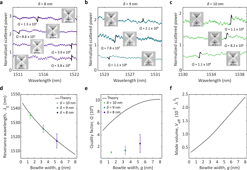
We characterize the resonant modes of the self-assembled nanobeam cavities by cross-polarized far-field resonant scattering, which results in Fano resonances due to the interference with a vertical mode of the structure 5. Representative spectra of sets of nominally identical cavities for offsets = 8, 9 and 10 nm are shown in Figs. 4a-c. The resonant wavelengths and quality factors of the cavity modes are extracted by fitting Fano lineshapes to the observed resonant features (see Supplementary Section S4.1). We measure quality factors between and . The resonance wavelengths exhibit a clear red-shift with increasing offset, i.e., decreasing bowtie width. We estimate the average bowtie width in the measured cavities from the offset-to-width correspondence found via image analysis on a large set of SEM images of structures fabricated with = {0,7,14,20} nm (see Supplementary Section 3.2). The values for = 8, 9, and 10 nm correspond to = 5.3, 3.3 and 1.3 nm, respectively. We simulate the fabricated geometry, which includes a 2 nm native oxide layer (see Supplementary Section S2.2), for varying bowtie width and correlate the simulated and measured resonant wavelengths. Figure 4d shows both the measured and simulated resonant wavelength as a function of bowtie width, confirming the pronounced red shift with bowtie width. Spectral shifts between theory and experiment stemming from systematic errors in SEM measurements, local variations in the thickness of the device layer, etc. are commonly observed when analyzing nanocavities. In our case, we obtain an excellent agreement after red-shifting the theoretical curve by 15 nm. The measured -factors are smaller than the simulated values, as shown in Fig. 4e, mainly as a result of scattering losses due to structural disorder. Still, we consistently observe -factors exceeding previous experimental results on sub-diffraction confinement by more than an order of magnitude across multiple devices, even for 2 nm cavities that exhibit much smaller mode volumes than any previous experiments on dielectric cavities 5, 29 (see Fig. 4f). The high quality factors and the high process yield confirm the robustness of the surface-force self-assembly method.
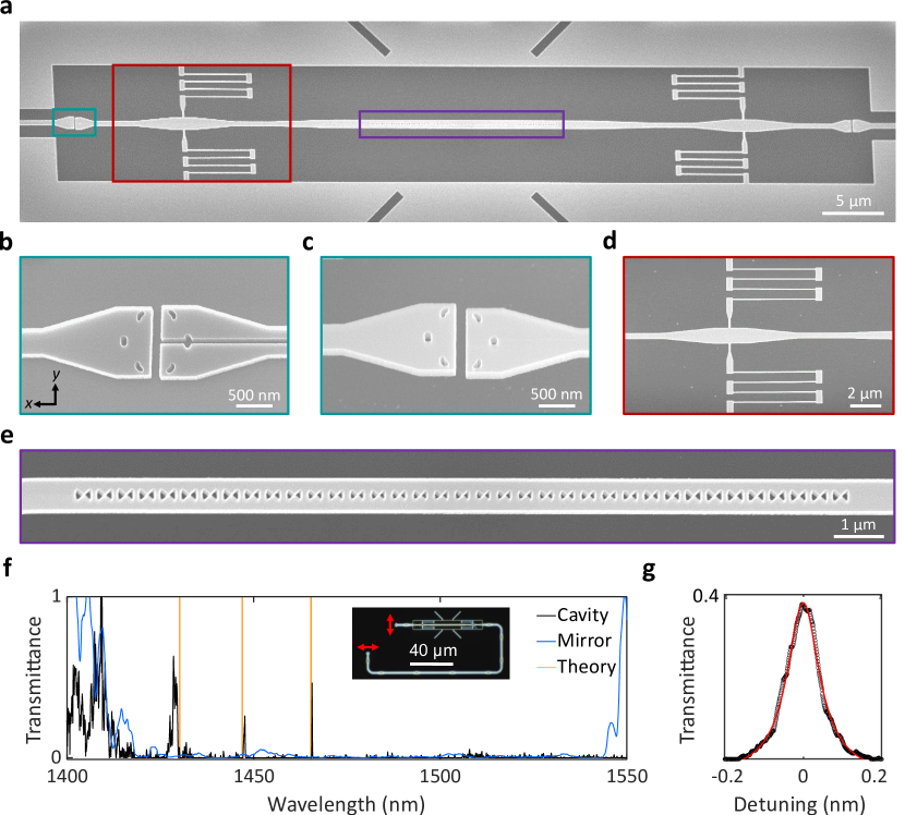
Finally, we turn to the quest of interfacing self-assembled devices with complex circuitry, i.e., the scalability of our method for interfacing the bottom-up self-assembled devices with top-down planar technology. For photonic-crystal nanobeam cavities, the most well-known approaches are either evanescent side-coupling 53 or (in-line) direct coupling 54. These two strategies are less trivial to realize for self-assembled devices since they require efficient coupling between mechanically isolated self-assembled regions such as a nanobeam cavity and non-self-assembled regions such as suspended waveguides. To this end, we use a recently invented topology-optimized photonic component that enables a broadband waveguide-to-waveguide transmission window across a 100 nm air trench, which provides both electrical and mechanical isolation 55. This enables the use of the self-assembly method by fabricating one of the sides of the component across the trench in two halves, which self-assembles at the same time as the nanobeam cavity. A self-assembled nanobeam cavity, including efficient interfaces to external waveguides via such circuit crossings and low-loss anchor points for the springs on tapered waveguide regions is shown in Fig. 5a. Figures 5b and c show tilted SEM images of the circuit crossing before and after self-assembly. The in-plane directed self-assembly is accurate down to the resolution of the SEM. Still, some out-of-plane bowing is observed, which could readily be avoided by adding more springs or other means of stress-release management. As in the structures in Fig. 2, two sets of springs are used, but they are attached to the tapered waveguide section as shown in Fig. 5d. The taper works as a mode expander that minimizes the field intensity at the silicon edges, allowing a calculated transmission of 99.7 % at the resonance wavelength of the cavity. Compared to the cavity shown in Fig. 2, the cavity for on-chip transmission experiments, which is shown in Fig. 5e, has a longer defect region to reduce out-of-plane radiation losses and a smaller number of mirror unit cells to facilitate efficient transmission through the cavity.
The photonic circuits beyond the crossings include two orthogonally oriented free-space grating couplers that allow measuring the circuit transmission through spatially resolved and cross-polarized spectroscopy 56 as shown by the dark-field optical microscope image in the inset of Fig. 5f (see Supplementary Section S4.2 for an SEM image of a full device). The cavity transmittance is obtained by normalizing the measured transmitted power to that measured in a self-assembled suspended waveguide of equivalent length, i.e., all optical elements on the chip and in the optical setup are factored out (see Supplementary Section S4.2). Figure 5f shows the transmittance for two different self-assembled devices: First, a 2 nm air-bowtie nanobeam cavity with 8 mirror unit cells and, second, a 2 nm air-bowtie nanobeam mirror with 25 identical unit cells, both corresponding to structures with = 12 nm for the employed sample. The transmittance of the mirror is negligible between 1425 nm and 1540 nm, which is consistent with the simulated photonic band gap. The spectrum of the cavity device exhibits three distinct Lorentzian resonances which agree quantitatively with our numerical cavity model using the fabricated dimensions (2 nm air bowties and a 2 nm native oxide layer), provided the wavelength of the simulated eigenmodes are shifted by 11.6 nm. This is well within the differences between experiments and theory commonly observed in nanophotonic devices based on the same top-down nanofabrication process 56 and in close agreement with the 15 nm shift employed for Fig. 4d. We observe a 39% cavity transmittance, which is smaller than the simulated value of 96.4% due to structural disorder (see Supplementary Section S4.2). The transmittance across the fundamental cavity mode is shown in Fig. 5g, and exhibits an irregular lineshape due to interference from reflection at the input and output grating couplers. By fitting to a Lorentzian lineshape, we obtain a of , comparable to the values obtained in Fig. 4 but with the notable difference that this is a loaded -factor and the cavity is efficiently coupled to a waveguide architecture.
Conclusion
Our mapping of the phase space governing the collapse of suspended platforms provides a clear design rule both for new research aiming to exploit the deterministic self-assembly and for conventional micro- and nanoelectromechanical systems, where collapses are generally undesirable. Looking ahead, the introduction of a robust and accurate self-assembly method in planar technology opens perspectives for a wide range of research that seemed far beyond experimental reach until now. While we focus here on the role of atomic-scale nanometer void features, which may be used for solid-state nanopore sequencing 57, nanogap quantum tunneling electrodes for biosensing 58 or as ultra-high quality shadow-masks for superconducting quantum electronic devices 59, lateral atomic-layer deposition before self-assembly might enable the formation of embedded atomic-scale structures for surface-enhanced Raman spectroscopy 23 or single-photon nonlinearities 60, 32. In this respect, our demonstration of optical cavities with atomic-scale features is the first step towards a new generation of nanophotonic and quantum photonic devices. For example, our self-assembled waveguide-coupled cavity features an unprecedented set of parameters: With a mode volume of cubic wavelengths and a loaded -factor of , the light-matter interaction is enhanced by a Purcell factor of over a bandwidth of 14 GHz and with a high on-resonance transmission. By incorporating embedded emitters such as erbium-doped alumina deposited with atomic-layer deposition 61, highly efficient single-photon sources at telecom wavelengths may be envisioned, possibly even with a high degree of quantum coherence due to the extreme Purcell enhancements. Such cavities may also enhance the bulk non-linearity of the embedded materials to a level where they could operate using single photons 32 and provide record single-photon optomechanical readout rates for gigahertz mechanical modes even in the absence of embedded materials 34. More generally, our work opens perspectives for exploring new regimes of photonics, electronics, and mechanics at atomic scales while at the same time enabling scalable and self-aligned integration with large-scale chip architectures.
Methods
Fabrication process
The devices are fabricated on a commercial silicon-on-insulator substrate (Soitec) with a 220 nm-thick silicon device layer and a 2 µm-thick buried oxide layer. A two-layer hardmask is deposited on the silicon device layer, consisting of 30 nm poly-crystalline chromium and 12 nm poly-crystalline silicon layers, followed by a 50 nm layer of chemically semi-amplified resist (CSAR) applied by spin-coating. The patterns are exposed in the resist with a 100 keV 100 MHz JEOL9500FSZ electron-beam writer and transferred into the silicon device layer by a low-power switched reactive-ion etch. The buried oxide layer is selectively etched to suspend the devices with an anhydrous hydrofluoric-acid (99.995%) vapour phase etcher (SPTS Primaxx uEtch), using ethanol as a catalyst. A process pressure of 131 Torr, and a slow etching recipe (etch rate of approximately 14 nm/min) are used for selective oxide etching. The fabrication process flow is detailed in Ref. 5, and the hardmask etching process is detailed in Refs. 62, 56.
Surface-force characterization
The measurements in Fig. 1 are performed on Sample A (1536 devices) with platforms of widths = [2, 3, 4, 5, 8, 16, 32, 64] µm with logarithmic variations of both and from 30 to 200 nm and from 0.0097 to 13 N/m, respectively. The silicon-on-insulator stack sets the thickness of the platform and height above the substrate to = 220 nm and = 2 µm, respectively. A 1 µm pitch, array of 200 nm sidelength square is etched in the platform to facilitate the underetching. The devices also have trenches on the top-right and top-left of the platform to reduce potential fringing-field contributions to the surface forces 63. Scales are integrated on the right and left side of the platforms to measure displacements due to the built-in stress release, which imposes a baseline correction to the initial gap (see Supplementary Section S1.1). All these additional features have minimal effect on whether the devices collapse or not collapse.
Scanning transmission-electron microscope
Annular dark-field STEM imaging is performed using an FEI Titan 80-300 kV transmission electron microscope (TEM) operated at 300 kV to extract high-resolution images of the cavity bowtie region. The transmission electron microscope is fitted with a field-emission gun and an aberration-correction unit on the probe-forming lenses, giving it a spatial resolution better than 0.1 nm. A focused ion beam is used inside a FIB-SEM system (Helios Nanolab 600) to prepare the cavity structures for high-resolution imaging. A micromanipulator needle is welded to the cavity structure by induced deposition of Pt from a precursor source to transport the cavities from the sample to the TEM equipment. This is followed by cutting the tethers around the cavities using a Ga+ ion beam of 30 keV and 40 pA current, lifting the released cavities from the sample, relocating and welding the cavities to a TEM-compatible Cu grid, and finally detaching the micromanipulator needle from the cavities using the ion beam.
Optical measurements
The optical spectrum of each nanocavity is measured using free-space confocal microscopy. Measurements are performed either by direct resonant scattering on isolated nanocavities (Fig. 4) or via transmission by coupling light in and out of photonic circuits with embedded nanocavities (Fig. 5). Two fiber-coupled tunable diode lasers (Santec TSL-710, = 1355 - 1480 nm and = 1480 - 1640 nm) are combined into a 4x1 optical switch (Santec OSU-110) for excitation of the nanocavities. Light is focused onto and collected from the sample using a 50X microscope objective (Mitutoyo Plan Apo NIR 50X, NA = 0.42). For resonant scattering measurements, the excitation and collection spots spatially overlap, and their polarizations are set at relative to the leading polarization of the cavity mode and orthogonal to each other (see Supplementary Section S4.1 for the schematic). For measurements of nanocavities embedded in photonic circuits, the excitation and collection are cross-polarized and spatially offset by employing two free-space grating couplers oriented orthogonal to each other. Both the grating couplers are kept 30 µm apart in vertical and horizontal directions. Spectra are acquired by sequentially sweeping the two tunable lasers (if needed) and detecting with a synchronous calibrated power meter (Santec MPM-210). The spectra are then normalized to the laser spectrum as measured with a direct patch fiber for resonant scattering measurements and to the spectrum of a suspended silicon waveguide of equivalent length for the photonic circuits.
Acknowledgements
We thank Marcus Albrechtsen for valuable discussions. The authors gratefully acknowledge financial support from the Villum Foundation Young Investigator Programme (Grant No. 13170), Innovation Fund Denmark (Grant No. 0175-00022 – NEXUS and Grant No. 2054-00008 – SCALE), the Danish National Research Foundation (Grant No. DNRF147 – NanoPhoton), Independent Research Fund Denmark (Grant No. 0135-00315 – VAFL), the European Research Council (Grant. No. 101045396 – SPOTLIGHT), and the European Union’s Horizon 2021 research and innovation programme under a Marie Sklodowska-Curie Action (Grant No. 101067606 – TOPEX).
Author contributions
A.N.B. and T.A.S. fabricated the devices and did the SEM characterization. A.N.B. and G.A. did the optical characterization. B.V.L, A.N.B, G.A. and K.T. did the numerical design and analysis. S.K. did the STEM measurements. A.N.B., T.A.S., and G.A. did the data analysis. A.N.B., G.A., and S.S. prepared the manuscript with input from all authors. S.S., B.V.L., and K.T. designed the experiment. S.S. conceived, initiated and supervised the project with co-supervision by B.V.L and G.A.
Data availability
The data that supports this manuscript is available upon reasonable request.
Competing financial interests
The authors declare no competing financial interests.
References
- [1] Winfree, E., Liu, F., Wenzler, L. A. & Seeman, N. C. Design and self-assembly of two-dimensional DNA crystals. Nature 394, 539–544 (1998).
- [2] Heiss, M. et al. Self-assembled quantum dots in a nanowire system for quantum photonics. Nat. Mater. 12, 439–444 (2013).
- [3] Sun, Z. et al. Generalized self-assembly of scalable two-dimensional transition metal oxide nanosheets. Nat. Commun. 5, 1–9 (2014).
- [4] Klimchitskaya, G., Mohideen, U. & Mostepanenko, V. The Casimir force between real materials: Experiment and theory. Rev. Mod. Phys. 81, 1827 (2009).
- [5] Albrechtsen, M. et al. Nanometer-scale photon confinement in topology-optimized dielectric cavities. Nat. Commun. 13, 6281 (2022).
- [6] Aoyama, H. et al. The International Roadmap For Devices And Systems (IEEE, 2022); https://irds.ieee.org/images/files/pdf/2022/2022IRDS_Litho.pdf.
- [7] Koenderink, A. F., Alù, A. & Polman, A. Nanophotonics: Shrinking light-based technology. Science 348, 516–521 (2015).
- [8] Lodahl, P., Mahmoodian, S. & Stobbe, S. Interfacing single photons and single quantum dots with photonic nanostructures. Rev. Mod. Phys. 87, 347 (2015).
- [9] Hah, J. H. et al. Converging lithography by combination of electrostatic layer-by-layer self-assembly and 193 nm photolithography: Top-down meets bottom-up. J. Vac. Sci. Technol. B 24, 2209–2213 (2006).
- [10] Min, Y., Akbulut, M., Kristiansen, K., Golan, Y. & Israelachvili, J. The role of interparticle and external forces in nanoparticle assembly. Nat. Mater. 7, 527–538 (2008).
- [11] Grzelczak, M., Vermant, J., Furst, E. M. & Liz-Marzán, L. M. Directed self-assembly of nanoparticles. ACS Nano 4, 3591–3605 (2010).
- [12] Wang, L. et al. High performance 33.7 GHz surface acoustic wave nanotransducers based on AlScN/diamond/Si layered structures. Appl. Phys. Lett. 113, 093503 (2018).
- [13] Marsili, F. et al. Single-photon detectors based on ultranarrow superconducting nanowires. Nano Lett. 11, 2048–2053 (2011).
- [14] Chao, W., Harteneck, B. D., Liddle, J. A., Anderson, E. H. & Attwood, D. T. Soft X-ray microscopy at a spatial resolution better than 15 nm. Nature 435, 1210–1213 (2005).
- [15] Deamer, D., Akeson, M. & Branton, D. Three decades of nanopore sequencing. Nat. Biotech. 34, 518–524 (2016).
- [16] Liu, F. et al. Sculpting extreme electromagnetic field enhancement in free space for molecule sensing. Small 14, 1801146 (2018).
- [17] Wang, J. et al. Multidimensional quantum entanglement with large-scale integrated optics. Science 360, 285–291 (2018).
- [18] Liu, Y. et al. Promises and prospects of two-dimensional transistors. Nature 591, 43–53 (2021).
- [19] Chung, S. E., Park, W., Shin, S., Lee, S. A. & Kwon, S. Guided and fluidic self-assembly of microstructures using railed microfluidic channels. Nat. Mater. 7, 581–587 (2008).
- [20] Zhang, S. Fabrication of novel biomaterials through molecular self-assembly. Nat. biotechnology. 21, 1171–1178 (2003).
- [21] Thiele, S. et al. Electrically driven nuclear spin resonance in single-molecule magnets. Science 344, 1135–1138 (2014).
- [22] Zhang, K. et al. A Gd@C82 single-molecule electret. Nat. Nanotechnol. 15, 1019–1024 (2020).
- [23] Luo, S. et al. High-Throughput Fabrication of Triangular Nanogap Arrays for Surface-Enhanced Raman Spectroscopy. ACS Nano (2022).
- [24] Ouk Kim, S. et al. Epitaxial self-assembly of block copolymers on lithographically defined nanopatterned substrates. Nature 424, 411–414 (2003).
- [25] Duan, H., Fernández-Domínguez, A. I., Bosman, M., Maier, S. A. & Yang, J. K. Nanoplasmonics: classical down to the nanometer scale. Nano Lett. 12, 1683–1689 (2012).
- [26] Kim, I., Mun, J., Hwang, W., Yang, Y. & Rho, J. Capillary-force-induced collapse lithography for controlled plasmonic nanogap structures. Microsyst. Nanoeng. 6, 1–9 (2020).
- [27] Palstra, I. M., Doeleman, H. M. & Koenderink, A. F. Hybrid cavity-antenna systems for quantum optics outside the cryostat? Nanophotonics 8, 1513–1531 (2019).
- [28] Gondarenko, A. et al. Spontaneous Emergence of Periodic Patterns in a Biologically Inspired Simulation of Photonic Structures. Phys. Rev. Lett. 96, 143904 (2006).
- [29] Albrechtsen, M., Vosoughi Lahijani, B. & Stobbe, S. Two regimes of confinement in photonic nanocavities: bulk confinement versus lightning rods. Opt. Express 30, 15458–15469 (2022).
- [30] Wu, H. et al. Photonic Nanolaser with Extreme Optical Field Confinement. Phys. Rev. Lett. 129, 013902 (2022).
- [31] Mork, J. & Yvind, K. Squeezing of intensity noise in nanolasers and nanoLEDs with extreme dielectric confinement. Optica 7, 1641–1644 (2020).
- [32] Choi, H., Heuck, M. & Englund, D. Self-Similar Nanocavity Design with Ultrasmall Mode Volume for Single-Photon Nonlinearities. Phys. Rev. Lett. 118, 223605 (2017).
- [33] Nozaki, K. et al. Sub-femtojoule all-optical switching using a photonic-crystal nanocavity. Nat. Photon. 4, 477–483 (2010).
- [34] Bozkurt, A., Joshi, C. & Mirhosseini, M. Deep sub-wavelength localization of light and sound in dielectric resonators. Opt. Express 30, 12378–12386 (2022).
- [35] Chao, P., Strekha, B., Kuate Defo, R., Molesky, S. & Rodriguez, A. W. Physical limits in electromagnetism. Nat. Rev. Phys. 4, 543–559 (2022).
- [36] Panuski, C., Englund, D. & Hamerly, R. Fundamental thermal noise limits for optical microcavities. Phys. Rev. X 10, 041046 (2020).
- [37] Mortensen, N. A., Raza, S., Wubs, M., Søndergaard, T. & Bozhevolnyi, S. I. A generalized non-local optical response theory for plasmonic nanostructures. Nat. Commun. 5, 1–7 (2014).
- [38] Bharadwaj, S., Van Mechelen, T. & Jacob, Z. Picophotonics: Anomalous atomistic waves in silicon. Phys. Rev. Appl. 18, 044065 (2022).
- [39] Hollenbach, M. et al. Wafer-scale nanofabrication of telecom single-photon emitters in silicon. Nat. Commun. 13, 7683 (2022).
- [40] Buks, E. & Roukes, M. Stiction, adhesion energy, and the Casimir effect in micromechanical systems. Phys. Rev. B 63, 033402 (2001).
- [41] Munkhbat, B., Canales, A., Küçüköz, B., Baranov, D. G. & Shegai, T. O. Tunable self-assembled Casimir microcavities and polaritons. Nature 597, 214–219 (2021).
- [42] Palasantzas, G. & Svetovoy, V. B. Problems in measuring the Casimir forces at short separations. Int. J. Mod. Phys. A. 37, 2241001 (2022).
- [43] Rodriguez, A. W., Capasso, F. & Johnson, S. G. The Casimir effect in microstructured geometries. Nat. Photon. 5, 211–221 (2011).
- [44] Burger, F. A., Corkery, R. W., Buhmann, S. Y. & Fiedler, J. Comparison of theory and experiments on van der waals forces in media—a survey. J. Phys. Chem . C. 124, 24179–24186 (2020).
- [45] Midolo, L., Schliesser, A. & Fiore, A. Nano-opto-electro-mechanical systems. Nat. Nanotechnol. 13, 11–18 (2018).
- [46] Behunin, R., Intravaia, F., Dalvit, D., Neto, P. M. & Reynaud, S. Modeling electrostatic patch effects in Casimir force measurements. Phys. Rev. A 85, 012504 (2012).
- [47] Gies, H. & Klingmüller, K. Casimir edge effects. Phys. Rev. Lett. 97, 220405 (2006).
- [48] Lamoreaux, S. K. Demonstration of the Casimir Force in the 0.6 to 6 m range. Phys. Rev. Lett. 78, 5 (1997).
- [49] Lin, K.-L. et al. Phase identification using series of selected area diffraction patterns and energy dispersive spectrometry within TEM. Microsc. Res. 2, 57 (2014).
- [50] Nasr Esfahani, M. et al. Effect of native oxide on stress in silicon nanowires: Implications for nanoelectromechanical systems. ACS Appl. Nano Mater. 5, 13276–13285 (2022).
- [51] Creatore, C., Andreani, L. C., Miritello, M., Lo Savio, R. & Priolo, F. Modification of Erbium radiative lifetime in planar silicon slot waveguides. Appl. Phys. Lett. 94, 103112 (2009).
- [52] Galli, M. et al. Strong enhancement of Er 3+ emission at room temperature in silicon-on-insulator photonic crystal waveguides. Appl. Phys. Lett. 88, 251114 (2006).
- [53] Afzal, F. O., Halimi, S. I. & Weiss, S. M. Efficient side-coupling to photonic crystal nanobeam cavities via state-space overlap. JOSA B 36, 585–595 (2019).
- [54] Quan, Q., Deotare, P. B. & Loncar, M. Photonic crystal nanobeam cavity strongly coupled to the feeding waveguide. Appl. Phys. Lett. 96, 203102 (2010).
- [55] Vosoughi Lahijani, B. et al. Electronic-photonic circuit crossings. Preprint at https://arXiv:2204.14257 (2022).
- [56] Rosiek, C. A. et al. Observation of strong backscattering in valley-Hall photonic topological interface modes. Preprint at https://arXiv:2206.11741 (2022).
- [57] Xue, L. et al. Solid-state nanopore sensors. Nat. Rev. Mater. 5, 931–951 (2020).
- [58] He, Q. & Tang, L. Sub-5 nm nanogap electrodes towards single-molecular biosensing. Biosens. Bioelectron. 114486 (2022).
- [59] Delaney, R. et al. Superconducting-qubit readout via low-backaction electro-optic transduction. Nature 606, 489–493 (2022).
- [60] Raza, A. et al. ALD assisted nanoplasmonic slot waveguide for on-chip enhanced Raman spectroscopy. APL Photonics 3, 116105 (2018).
- [61] Ronn, J. et al. Atomic layer engineering of Er-ion distribution in highly doped Er:Al2O3 for photoluminescence enhancement. ACS Photonics 3, 2040–2048 (2016).
- [62] Arregui, G. et al. Cavity Optomechanics with Anderson-Localized Optical Modes. Phys. Rev. Lett. 130, 043802 (2023).
- [63] Tsoukalas, K., Vosoughi Lahijani, B. & Stobbe, S. Impact of transduction scaling laws on nanoelectromechanical systems. Phys. Rev. Lett. 124, 223902 (2020).