Anomalous interfacial electron transfer kinetics in twisted trilayer graphene caused by layer-specific localization
Abstract
Interfacial electron-transfer (ET) reactions underpin the interconversion of electrical and chemical energy. Pioneering experiments showed that the ET rate depends on the Fermi–Dirac distribution of the electronic density of states (DOS) of the electrode, formalized in the Marcus–Hush–Chidsey (MHC) model. Here, by controlling interlayer twists in well-defined trilayer graphene moirés, we show that ET rates are strikingly dependent on electronic localization in each atomic layer, and not the overall DOS. The large degree of tunability inherent to moiré electrodes leads to local ET kinetics that range over three orders of magnitude across different constructions of only three atomic layers, even exceeding rates at bulk metals. Our results demonstrate that beyond the ensemble DOS, electronic localization is critical in facilitating interfacial ET, with implications for understanding the origin of high interfacial reactivity typically exhibited by defects at electrode–electrolyte interfaces.
Introduction
Interfacial electron-transfer reactions underpin the interconversion of electrical and chemical energy[1, 2, 3]. Within the microscopic theory of electron transfer, the MHC model[4, 5, 6, 7, 8, 4, 5] highlights the dependence of electrochemical rates on the DOS of an electrode, motivating the discovery of new approaches to manipulating the band structure of electrodes as a means of controlling the performance limits of energy conversion and storage devices. However, it is conventionally assumed that the electrode DOS are invariant with energy/overpotential and delocalized[8]. Atomic defects at electrode surfaces provide a striking, albeit challenging to control, example of the pronounced effect of local structural/electronic modifications on interfacial reactivity. Atomic vacancies[9], kinks, and step edges[10, 11, 12] are typically associated with massively enhanced interfacial reactivity compared to atomically pristine surfaces. The effect of these defects is typically explained in the context of providing increased DOS at energies that are desirable for charge transfer or formation of a surface-bound catalytic intermediate (such as mid-gap states in a semiconducting material[10, 9]). However, the dangling bonds at such sites would invariably introduce a strong spatial localization of these large electronic DOS. For this reason, beyond the augmented DOS magnitude, we might consider that localization may play a key role in facilitating interfacial ET to the necessarily localized electronic states on the solution-phase molecule/complex/ion. Yet, a systematic experimental examination of the effects of electronic localization on heterogeneous interfacial charge transfer has been intractable owing to the considerable synthetic challenge of constructing pristine electrode materials that would allow a deterministic modulation of this property separate from the overall DOS.
Azimuthal misalignment of atomically thin layers produces moiré superlattices and alters the electronic band structure, in a manner that is systematically dependent on the interlayer twist angle[13, 14]. The formation of flat electronic bands, particularly at a series of ‘magic’ moiré angles leads to a diversity of correlated electron physics[15, 16, 17, 18]. Notably, these flat bands imply a large DOS that is highly localized in real space[19]. Small-angle twisted bilayer graphene (TBG) exhibits a recently discovered angle-dependent electrochemical behavior[20], where outer-sphere ET kinetics can be tuned nearly tenfold simply by varying moiré twist angle, , between 0° and 2°.
The stacking order of graphene in multilayers strongly alters the resulting electronic properties of the system[21, 23, 24, 25, 26, 27, 28, 29, 16, 22]. Where Bernal (ABA-stacked) trilayer graphene displays dispersive bands, rhombohedral (ABC) graphene possesses a non-dispersive, or ‘flat’, electronic band close to the Fermi level, which is responsible for the emergence of correlated electron phenomena at low temperatures[30, 31].
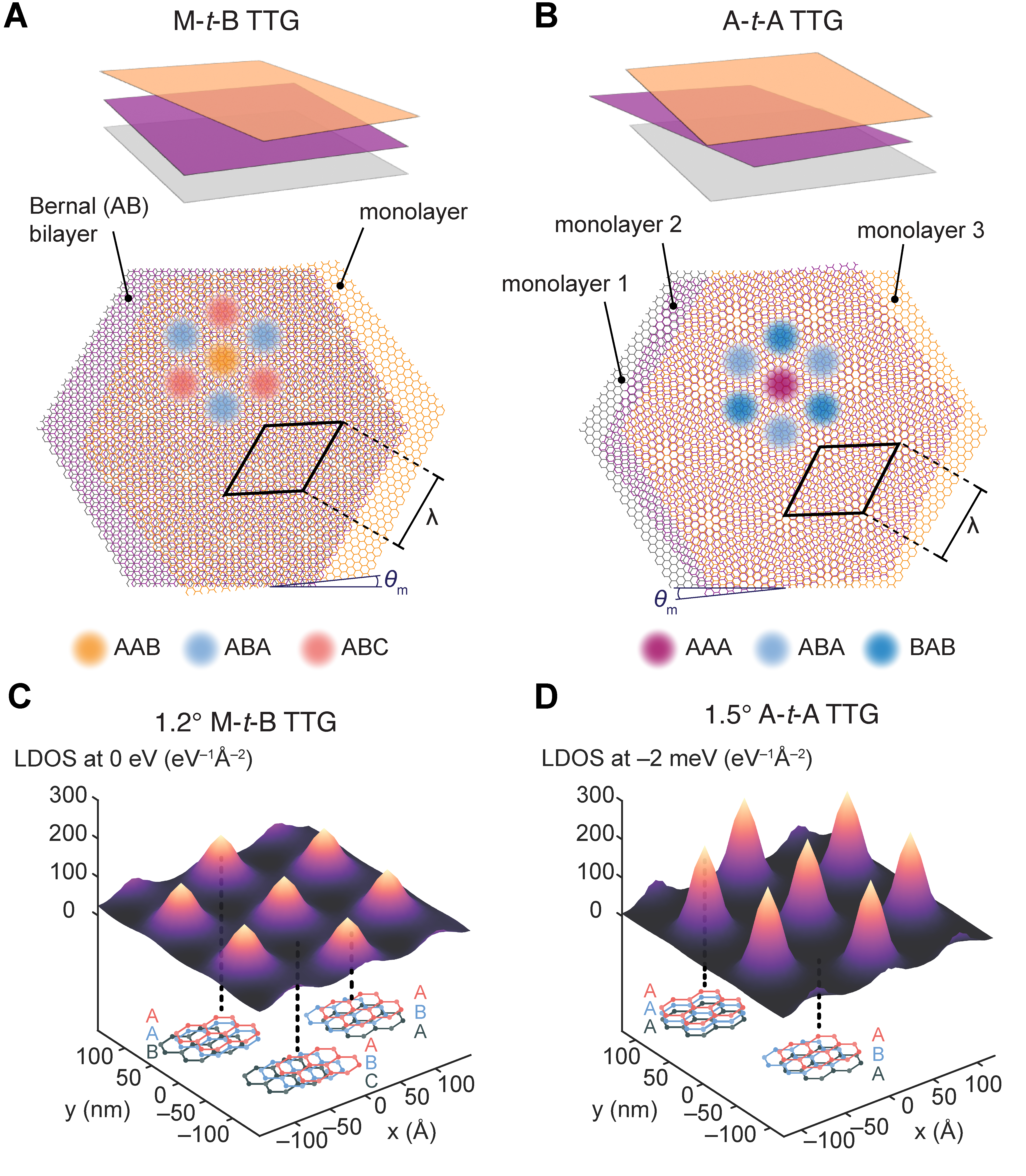
More pronounced flat bands are produced in twisted trilayer graphene (TTG) structures. Rotationally misaligned (by a moiré ‘twist’ angle ) monolayer and Bernal stacked bilayer forms a ‘monolayer-twist-bilayer’ (M-t-B) heterostructure (Fig. 1A)[32, 33]. Systematically alternating the angle between adjacent graphene layers such that the top layer is perfectly aligned with the bottom layer results in an ‘A-t-A’ heterostructure (Fig. 1B)[29, 16, 22] that possesses extremely flat bands at a magic angle around . These flattened electronic bands, which manifest as large DOS that are localized on AAB and AAA sites in M-t-B and A-t-A TTG, respectively (Figs. 1C,D), now introduce distinctive possibilities for systematically probing the dependence of interfacial ET on electronic structure generally and in particular, the effects of electronic localization. For example, even within the TTG family, larger DOS are found in A-t-A as compared to M-t-B near their respective magic angles (Figs. 1C,D), properties that naively might be expected to correlate with interfacial ET rates, based on MHC theory.
Results and Discussion
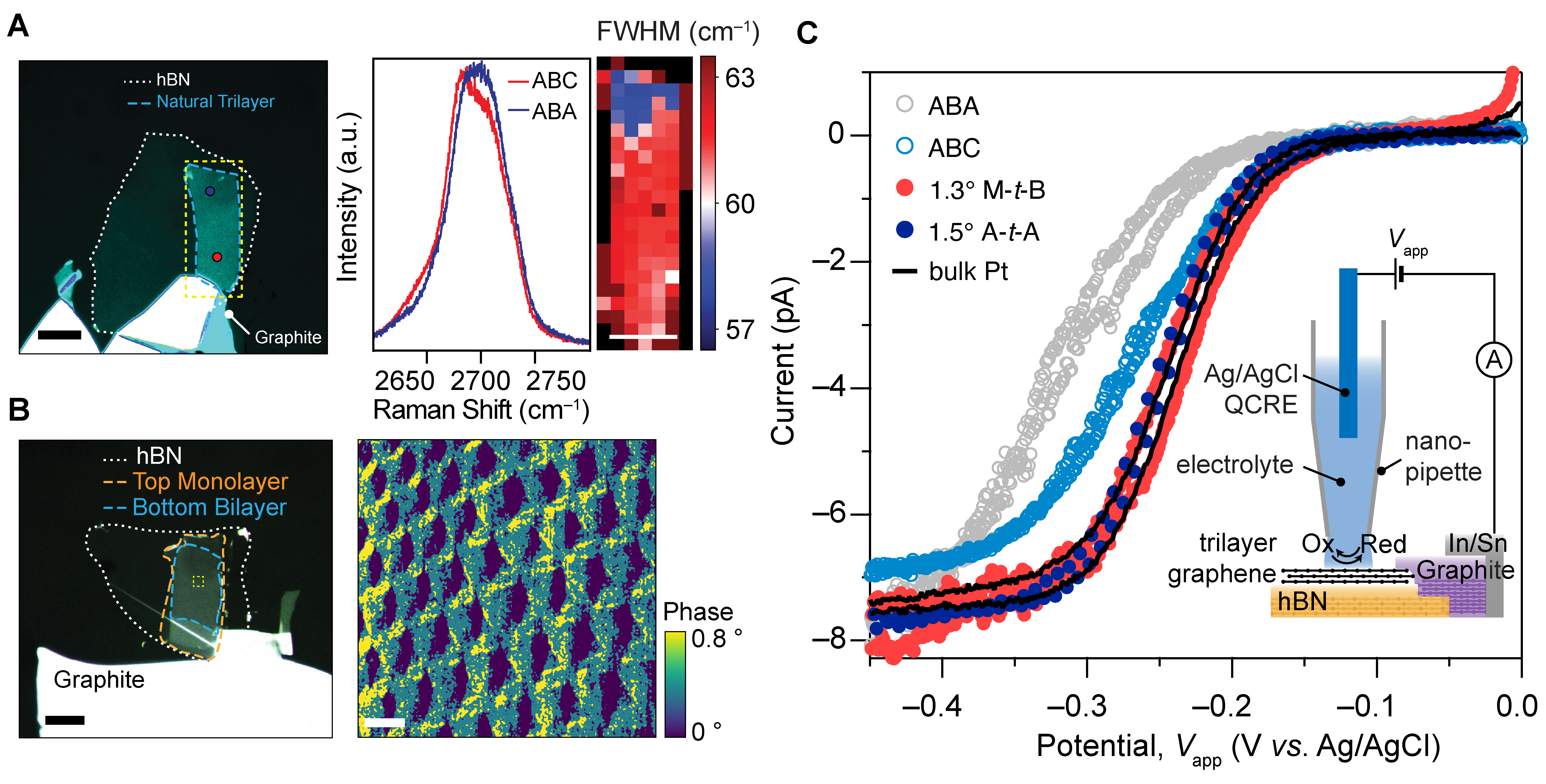
Scanning electrochemical cell microscopy (SECCM)[12] measurements were carried out on non-twisted (ABA, ABC) and twisted trilayer graphene samples that were fabricated into devices (see Methods)[20]. As shown in Fig. 2A, naturally occurring ABA and ABC trilayers were mechanically exfoliated from bulk graphite and identified using optical microscopy together with confocal Raman spectroscopy (see Methods) [34, 35]. M-t-B and A-t-A TTG samples were prepared by the ‘cut-and-stack’ approach (see Methods), resulting in samples possessing uniform around the ‘magic angles’ of about 1.34° for an M-t-B device and 1.53° for an A-t-A device. Piezoelectric force microscopy (PFM) and scanning tunneling microscopy (STM) were used to evaluate the twist angle distribution and uniformity across the moiré samples (Fig. 2B)[36]. Using SECCM, cyclic voltammograms (CVs) were measured with 2.0 mM \chRu(NH3)6^3+—an ideal and well-established redox couple for interrogating outer-sphere ET kinetics[11, 20]—and 0.10 M KCl as the supporting electrolyte. In Fig. 2C, a representative set of CVs collected from these different trilayer samples is shown. We find that the ABA domain of the flake shown in Fig. 2A exhibited the most sluggish rates of \chRu(NH3)6^3+ electro-reduction, evinced by a half-wave potential () of –0.32 V, which is cathodically shifted substantially from the equilibrium potential, , of –0.25 V for \chRu(NH_3)_6^3+/2+ (all potentials are reported relative to the Ag/AgCl quasi-counter/reference electrode). However, the measured from the CV acquired at region II (ABC domain) of the same flake was –0.27 V, pointing to considerably more facile electroreduction kinetics on the rhombohedral trilayer as compared to the Bernal trilayer. For both TTG samples, reversible CVs with –0.25 V were obtained, indicative of highly facile electrokinetics and heterogeneous electrochemical rate constants that exceed those of both ABA and ABC graphene considerably. These observations motivated the measurement of the variation of interfacial ET rates with .
To quantitatively assess differences in interfacial kinetics associated with disparate electronic structures, we compared experimental CVs to those simulated with different standard rate constants, , calculated with the Butler–Volmer model (see Methods). Here, it is critical to account for the relatively small and potential-dependent quantum capacitance, (see Methods)[20, 11] in these low-dimensional electrodes, which for a given applied potential, , produces a dynamic electron or hole doping of the few-layer graphene by an energy of (where is the elementary charge and is the chemical potential relative to the charge neutrality potential). The remainder, , persists as a drop across the electric double layer (so that ). was calculated for all trilayer systems (ABA, ABC, as well as M-t-B and A-t-A at various ) (Fig. 3A) using the respective computed band structures and DOS profiles (see Methods). The corresponding plots of as a function of are shown in Fig. 3B. Taken together, these data reveal that flat electronic bands result in a more significant fraction of partitioning into near the charge neutrality potential. Notably, as shown in Fig. 3A, changes in tune and ‘magic-angle’ () A-t-A displays higher than ‘magic-angle’ () M-t-B consistent with its overall greater DOS (Fig. 1D).
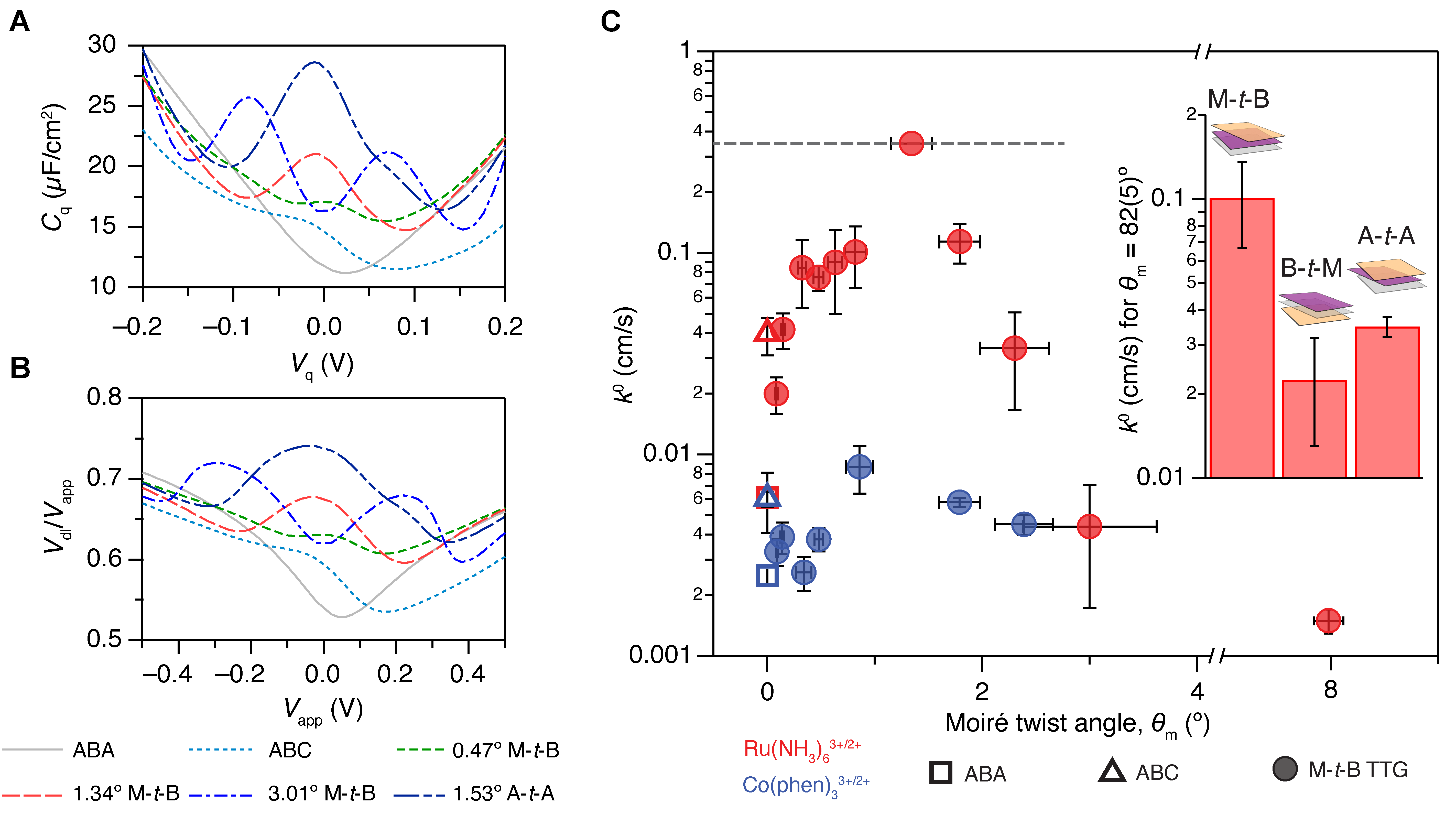
After determining in this manner, we extracted values by identifying the simulated CV that was in closest agreement with the experiment[20] (see Methods). The dependence of was measured by preparing M-t-B TTG devices with varying between 0.08° and 8.0° (see Methods) and acquiring CVs of \chRu(NH3)6^3+ electroreduction by SECCM for each sample. Fig. 3C shows the strong, non-monotonic variation in over two orders of magnitude from ABA and ABC graphene to M-t-B. For samples with 2° ET appears reversible within our accessible scan rates and so we cannot extract any kinetic information beyond noting that within this range of , cm/s. The quenched dependence of on (blue markers in Fig. 3C) in analogous electrochemical measurements of the trisphenanthroline cobalt(III/II) redox couple, \chCo(phen)_3^3+/2+ (see Methods) provides compelling evidence that it is the moiré flat bands that drive the observed angle-dependent electrokinetic modulation in TTG, as in TBG[20].
An unexpected observation of the factors controlling interfacial ET is made by comparing the electrochemical responses of TTG polytypes. A-t-A TTG, on the basis of its massive DOS (Fig. 1D) and giant —which exceeds that of M-t-B (Fig. 3A)—should be expected to yield the highest ET rates. However, while an effect of on is also observed in A-t-A samples, this variant of TTG displays consistently lower than M-t-B at similar (Fig. 3C, inset). Further, B-t-M heterostructures, which consist of a Bernal bilayer placed with a twist atop a monolayer (i.e., flipped versions of M-t-B), display markedly lower values than the corresponding M-t-B electrodes, notwithstanding an ostensibly identical overall electronic structure. These striking observations point clearly to effects governing the interfacial ET kinetics beyond simply the ensemble DOS.
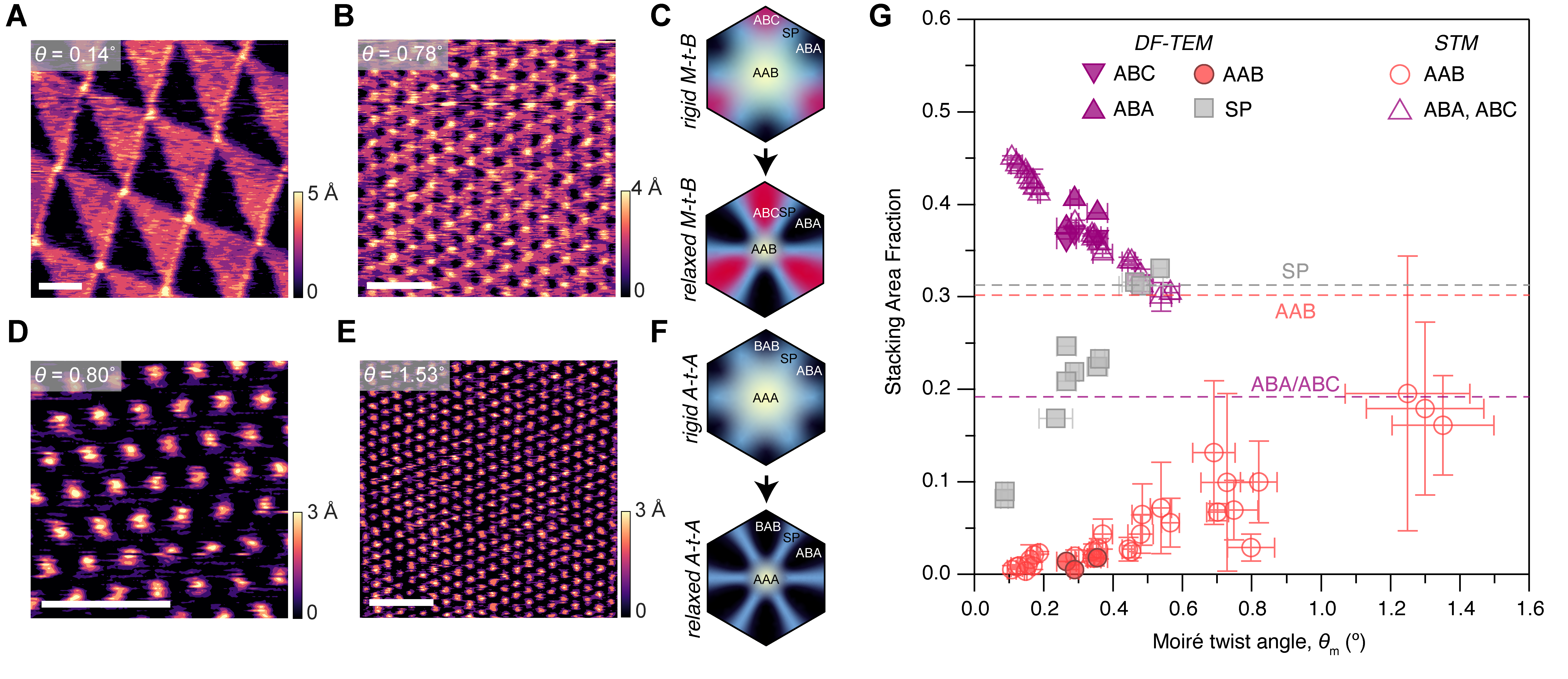
To fully understand these dependencies as well as the disparities between interfacial electron transfer kinetics of M-t-B, B-t-M, and A-t-A, we used STM (room temperature, constant current) to evaluate the role of lattice relaxation in controlling the area fraction of stacking domains in M-t-B and A-t-A TTG. In Fig. 4A, a representative STM map of small-angle () M-t-B shows a clear contrast between the various stacking domains. Regions with higher local DOS appear brighter than those with lower DOS since a larger tip–sample distance is required to maintain a constant current[33]. ABC domains, therefore, appear brighter than ABA domains owing to the native flatband of the ABC stacking type. These ABA and ABC domains (black and red regions, respectively) form alternating triangular patterns while the AAB region forms small circles of diameter 11 nm, which appear with the brightest contrast owing to the localization of the moiré flatband and associated large DOS on these AAB sites as shown in Fig. 1C (this is analogous to the localization of moiré flatbands on AA sites in TBG[19]). For (Fig. 4B), while the triangular ABA/ABC patterns have shrunk in size compared to those in Fig. 4A, the diameters of AAB regions remained largely unchanged. For A-t-A, AAA domains are visible as bright spots (Figs. 4D,E), consistent with the localization of the large DOS on these regions (Fig. 1D)[37], with degenerate ABA and BAB regions requiring smaller tip–sample distances (dark regions) to sustain a constant STM current because of a lower local DOS.
The measured area distribution of stacking domains in TTG, therefore, differ significantly from those of rigid moiré structures and are instead relaxed as depicted schematically in Fig 4C,F minimizing (maximizing) high (low) energy domains in a manner that is conceptually analogous to that reported for TBG[38, 19, 39]. To support these experiments, we also performed finite element method (FEM) simulations to model relaxation in TTG, finding results that lie in good agreement with our STM and dark-field transmission electron microscopy data. Importantly, these structural measurements and calculations permit a quantitative determination of the area fractions in TTG after reconstruction as a function of as plotted in Fig. 4G.
These area fraction distributions after structural relaxation explain the origin of the kinetic modulation observed in Fig. 3C at as being driven by -dependent area fractions of the ‘topological defect’[40, 41] AAB and AAA sites. Our relaxation simulations also show that at , relaxation of these moiré superlattices reestablishes nearly commensurate ABA, BAB, and/or ABC domains with local DOS that should not deviate substantially from those of freestanding ABA and ABC trilayers. This observation is in line with previous experimental[39, 38, 33, 41] and theoretical studies[42, 41] of lattice relaxation in bilayer analogues. Therefore, by considering variations at in Fig. 3C (which are also within the range of kinetically resolvable ), we can extract the local rate constant associated with the AAB and AAA stacking domains through Eq.1 and Eq.2 where and represent the area fraction and local standard heterogeneous electron transfer rate constant, respectively, for stacking domain .
| (1) |
| (2) |
As a result of the lattice relaxation effect discussed above, we can determine and from independent measurements of freestanding Bernal and rhombohedral trilayers (Figs. 2C and 3C). In addition, we can assume that , which is justified on the basis of the STM images and calculated local DOS. This analysis allows us to extract standard electron transfer rate constants for the AAB (M-t-B), ABB (B-t-M), and AAA (A-t-A) topological defects.
Combined with previous electrochemical measurements at TBG surfaces[20] we compare ET kinetics of \chRu(NH3)6^3+/2+ among a wide array of stacking configurations from monolayer to trilayer graphene in Fig. 5A. For atomic stacking orders naturally found in bulk graphite, we observed a gradual enhancement as the number of layers increases from monolayer to Bernal trilayer. This can be explained by a modest increase in DOS close to the Fermi level as the number of layers increases.[11] ABC graphene displays a pronounced augmentation in from that of ABA graphene associated with the intrinsic flat band of the rhombohedral system. Most notably, ‘artificial’ high energy stacking (AA, AAA, AAB, ABB) topological defects created by moiré superlattices exhibit extraordinarily high values, with that of AAB exceeding 3 cm/s, which is greater than that measured on bulk platinum electrodes ( cm/s)[43], notwithstanding only consisting of three atomic layers.
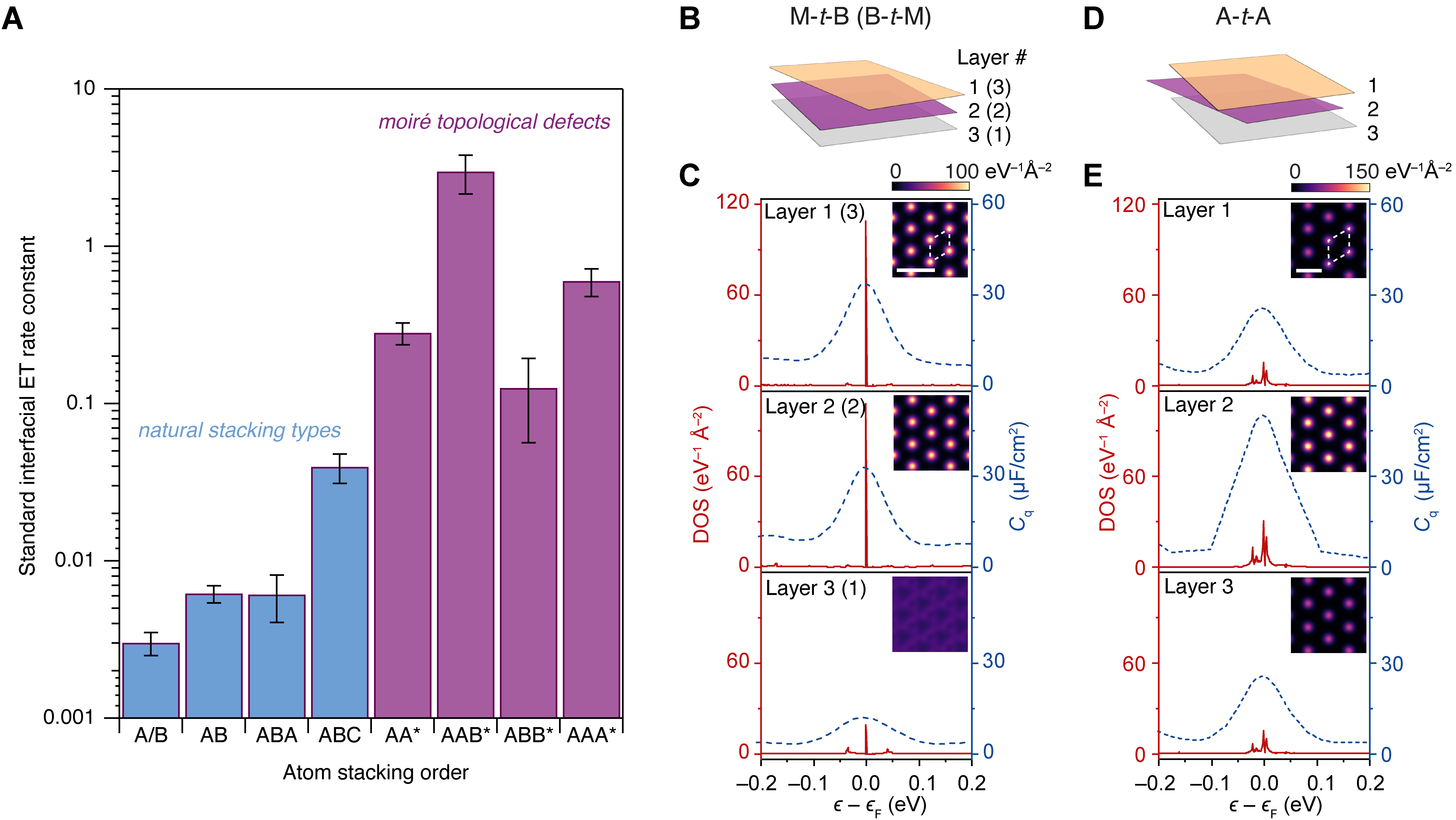
Fig. 5A also shows the unexpected result that AAA sites display lower ET rates than AAB notwistanding the higher DOS and of AAA than AAB (Fig. 3A). Strikingly, we also find that ABB sites yield slower ET kinetics than both AAB (despite identical overall DOS) and AA (despite higher overall DOS). Thus, while in-plane electronic localization and structural relaxation effects explain the dependence of on in TTG, the relative interfacial ET rates of AAB (M-t-B), ABB (B-t-M), and AAA (A-t-A) (Fig. 3C inset and Fig. 5A) appear not to correlate with DOS.
To explain these trends, Figs. 5C–E show layer-isolated local DOS() profiles (Figs. 5C,E) at the topological defects (AAB/ABB, AAA) along with calculated real-space DOS maps (insets in Figs. 5C,E). These calculations show how the DOS enhancements at AAB sites are distinctly localized on the top two layers of M-t-B structures (i.e. the ‘AA’ portions of AAB)[44]. In contrast, the DOS at AAA sites are most strongly localized on the middle layer of A-t-A. This three-dimensional electronic localization (within a thickness of only three atomic layers) arising from different symmetries of these topological defects unveils the fundamental basis for the unexpected trends in ET rate constants at AAB, ABB, and AAA (Figs. 3C and 5A): though the electrodes are only three atomic layers thick, ET rate constants are only correlated with the electronic properties precisely at the electrode–electrolyte interface.
These observations strongly hint at the role of interfacial electronic coupling (between the localized states on the electrode and the electron donor/acceptor in solution), electric double-layer effects, and/or interfacial reorganization energy as even more crucial than the overall DOS alone. Indeed, theoretical calculations based on the MHC model that accounts only for the -dependent DOS, but with a coupling strength, , and reorganization energy, , that are invariant with , vastly underestimate the dependence of on . These MHC calculations also likewise predict identical interfacial ET rates for M-t-B and B-t-M, which is clearly at odds with the experiment. Our experimental results, therefore, now motivate future theoretical work to adapt these MHC models to consider how electronic localization, which is deterministically tuned here by varying or TTG structure, modifies [45] — and/or [46], to bridge the gap between theory and experiment and extend our microscopic understanding of interfacial ET.
Conclusions
Controlling stacking geometries and twist angles in few-layer graphene therefore enables the manipulation of standard ET rate constants over three orders of magnitude. In particular, energetically unfavorable topological defects (AAA, AAB stacking domains), which are attainable only through the construction of a moiré superlattice, exhibit extraordinarily high standard rate constants. This electrochemical behavior arises from the moiré-derived flat bands that are localized in these topological defects. In addition to the effects of in-plane structural relaxation and electronic localization, the out-of-plane localization of the electron wavefunction on specific layers of twisted trilayer graphene results in measurable differences in ET rates at topological defects possessing different symmetries.
These results provide a powerful demonstration of the sensitivity of interfacial ET kinetics to the three-dimensional localization of electronic states at electrochemical surfaces, and raise the question of whether traditional measurements of ET rates at macroscopic electrodes might severely underestimate the true local rate constant, which may be mediated by atomic defects that strongly localize electronic DOS, at these interfaces. In turn, SECCM measurements are shown to be powerful tools for probing layer-dependent electronic localization in atomic heterostructure electrodes.
Future experimental and theoretical work is needed to shed more light on the microscopic origin of these electron-transfer modulations in the context of reorganization energy, electronic coupling, and even electric double-layer structure. This work also heralds the use of moiré materials as a versatile and systematically tunable experimental platform for theoretical adaptations of the Marcus–Hush–Chidsey framework applied to interfaces with localized electronic states, which are representative of defective surfaces that are ubiquitous to nearly all real electrochemical systems. In an applied context, twistronics is shown to be a powerful pathway for engineering pristine 2D material surfaces to execute charge transfer processes with facile kinetics, holding implications for electrocatalysis[47, 48] and other energy conversion device schemes that could benefit from ultrathin, flexible, and/or transparent electrodes that retain high electron-transfer kinetics.
Materials and Methods
Chemicals
Natural Kish graphite crystals were purchased from Graphene Supermarket. \chSi/SiO2 wafers (0.5 mm thick with 285 nm \chSiO2 or 90 nm \chSiO2) were purchased from NOVA Electronic Materials. Polydimethylsiloxane (PDMS) stamps were purchased from MTI Corporation. Sn/In alloy was purchased from Custom Thermoelectric. Poly(bisphenol-A carbonate) (Mw 45000), dichlorodimethylsilane (99.5%), hexaammineruthenium(III) chloride (98%), cobalt(II) chloride hexahydrate (98%), 1,10-phenanthroline (99%), calcium chloride (93%) and potassium chloride (99%) were purchased from Sigma-Aldrich and used as received. All aqueous electrolyte solutions were prepared with type I water (EMD Millipore, 18.2 M cm resistivity). The 2 mM solutions of tris(1,10-phenanthroline)cobalt(II) were prepared by dissolving 1:3 molar ratios of solid cobalt(II) chloride and 1,10-phenanthroline in water. In both \chRu(NH3)6^3+ and \chCo(phen)3^3+ solutions, 0.1 M of KCl was added as a supporting electrolyte.
Sample Fabrication
Graphite and hexagonal boron nitride (hBN) were exfoliated from the bulk crystals with Scotch tape. Exfoliated films were surveyed by an optical microscope (Laxco LMC-5000). Monolayer, bilayer and trilayer graphene were identified with their characteristic optical contrast of 7%, 12% and 18% respectively in the green channel[49]. Trilayer graphene films were further confirmed by Raman spectroscopy (HORIBA LabRAM Evo) of the 2D peak (around 2600 – 2700 cm-1)[34]. The 2D peak was used to distinguish different stacking domains (ABC/ABA) as ABC trilayer graphene exhibits an enhanced shoulder at around 2640 cm-1. Trilayer graphene and twisted trilayer graphene samples were fabricated by the well-established ‘cut and stack’ dry transfer method[20]. All transfers were done on a temperature-controlled heating stage (Instec), an optical microscope (Mitutoyo FS70) and a micromanipulator (MP-285, Sutter Instrument). For monolayer twist bilayer or bilayer twist monolayer samples, graphene flakes with both bilayer and monolayer parts were carefully selected. The monolayer section was severed from the bilayer with a scanning tunneling microscopy (STM) tip. For a-twist-a samples, a large piece of graphene ( 50 µm by 20 µm) was cut evenly into three pieces. A thin piece of poly(bisphenol-A carbonate) (PC) film ( 3 by 3 mm) attached to a PDMS chunk ( 7 by 7 mm) was used to pick up an hBN ( 10 – 20 nm) from the \chSiO2/Si substrate at 120 °C. This hBN was carefully aligned with the bottom layer of the graphene stack and lowered to pick up that piece. The stage was rotated (usually to a slightly larger angle than the desired twist) and the second piece of graphene was overlapped by the already picked-up graphene and thus delaminated from the substrate. For a-twist-a samples, a third piece of graphene was picked up after the stage was rotated back to the original orientation. A piece of graphite ( 20 nm, 50 µm by 50 µm) was then picked up such that it was connected to the graphene. The PC film was carefully removed from the PDMS and placed onto a clean \chSiO2/Si. In/Sn was painted onto the graphite via micro-soldering[50] to a metallic plate which is attached beneath the \chSiO2/Si.
Finite Element Simulation and Cyclic Voltammograms Fitting
All finite element simulations of electron transport were performed on COMSOL Multiphysics v5.6 (COMSOL) to capture the effects of quantum capacitance. The fitting of the CVs was achieved by statistical analysis of experimental and simulated CVs.
Raman Mapping
Confocal Raman spectra were collected by recording from 2550 – 2800 cm-1 with a 532 nm laser at 3.2 mW. Raman maps were generated by collecting spectrum across the trilayer films with a step size of 2 µm. The spectrum was fitted with single Lorentzian functions. The full-width half maxima of the fitted functions were used to differentiate ABA and ABC trilayers.
PFM Measurements
PFMs were performed on AIST-NT OmegaScope Reflection. Ti/Ir coated silicon probes from Nanosensor with a force constant of 2.8 Nm-1 and resonance frequency of 75 kHz were used. 2 V of AC bias with resonance frequencies at 820 kHz was used and the force was set at 25 nN.
STM Measurements
STM measurements were conducted using a Park NX10 STM module (Park Systems) at room temperature and atmospheric pressure. Pt-Ir tips were prepared by electrochemical etching of 0.25 mm Pt-Ir wires (Nanosurf) in 1.5 M \chCaCl2 solutions[51]. The scan images were taken with 0.2 V tip-sample bias and 100 pA current set point. Twist angles of various samples were determined using Delaunay triangulation on the Gaussian centers[20, 19].
Electron Microscopy Measurements
The transmission electron microscopy images of the nanopipettes were obtained with a JEOl 1200EX transmission electron microscope operated at 100 keV. The top 1 mm portion of the piette was attached to the grid (PELCO Hole Grids) such that the piette tip was positioned in the cetner hole, and the rest of the pipette was broken off. Selected area electron diffraction patterns were collected on a FEI Tecnai T20 S-TWIN transmission electron microscope with a LaB6 filament operated at 200 kV. Selected area electron diffraction was used to resolve the twist anlges for samples with twist angles larger than . To obtain the diffraction patterns, the fabricated TLG/hBN samples were measured at the National Center for Electron Microscopy facility in the Molecular Foundry at Lawrence Berkeley National Laboratory. Low-magnification DF-TEM images were acquired using a Gatan UltraScan camera on a Thermo Fisher Scientific Titan-class microscope operated at 60 kV.
Calculation of band structure and DOS
The DOS for trilayer graphene structures was calculated as a function of using the ab initio perturbation continuum model developed previously [52]. The low-energy electronic structure is based on a momentum expansion about the valley K point of the super-cell Brillouin zone, allowing a smooth dependence of bands on the twist angle. It has been shown that the perturbation continuum model exactly reproduces the results of the more expensive ab initio tight-binding model, and both are in good agreement with full density functional theory (DFT) calculations [52, 53, 54, 55]. The energy range of integration for the DOS was fixed at 0.5 eV around the charge neutrality point (CNP). For evaluation of the LDOS, the normalized moiré supercell was divided into a 90 90 grid in real space and sampled over 36 k points in the Brillouin zone. We kept the sublattice symmetry intact and assumed no extra screening of the interlayer coupling constants.
Quantum Capacitance Calculation
Quantum capacitance () describes the variation of electrical charges with respect to the chemical potential (). Theoretical values with respect to was calculated based on the following equation[56]:
| (3) |
| (4) |
where is the density of states, which we center at the CNP, is the thermal broadening function and is Boltzmann’s constant. We assumed = 300 K for our experimental conditions. The total electric double-layer capacitance is governed by the compact layer capacitance. Hence, we used a constant = 10 µF cm-2 to simplify the calculation [57]. We solved the self-consistent equations relating , , , and using Simpson integration and nonlinear least squares
| (5) |
| (6) |
to obtain vs. and vs. shown in Fig. 3.
SECCM Measurements
The SECCM nanopipettes were fabricated from single-channel quartz capillaries (inner and out diameters of 0.7 mm and 1.0 mm from Sutter Instrument) in a laser nano pipette puller (Sutter Instrument Model 2000). The program was set to heat 700, filament 4, velocity 20, delay 127 and pull 140 to generate pipettes of diameters around 200 nm, later confirmed with bright field TEM[20]. The outer surfaces of the pipettes were silanized by dipping them into dichlorodimethylsilane for 3 - 5 seconds when nitrogen flowed through the inside of the pipettes. They were then filled with either \chRu(NH3)6^3+ or \chCo(phen)3^3+ solutions through a micro syringe. The pipettes were gently tapped and a gentle string of nitrogen was used to eliminate the bubbles. The pipettes were then inserted with a silver AgCl wire as a quasi-counter reference electrode (QCRE). The pipettes were carefully approached (0.2 µm/s) to the locations of interest while a -0.5 V (0.5 V for \chCo(phen)3^3+) bias was applied. The meniscus achieved contact when a current of larger than 2 pA (or smaller than -2 pA) was observed. The pipette was allowed to stabilize for 30 s. Cyclic voltammograms (CVs) were then conducted by sweeping the potential at 100 mVs-1 between -0.6 to 0 V (0 to 0.8 V for \chCo(phen)3^3+/2+) for 5 cycles. Multiple CVs were collected for each sample and for small twist samples ( 0.15°) with moiré wavelengths of more than 80 nm, only CVs recorded with nanopipettes more than 200 nm in diameter were included to ensure they surveyed multiple stacking domains. To survey electrochemical activities across a large sample, the pipette was retracted by 1 µm after CVs were measured and horizontally moved to a new location for a new approach.
Acknowledgements
This material is based upon work supported by the US Department of Energy, Office of Science, Office of Basic Energy Sciences, under award no. DE-SC0021049 (experimental studies by K.Z., Y.Y., B.K., N.K., and D.K.B.) and the Office of Naval Research under award no. N00014-18-S-F009 (computational work by M.B. and V.V.). S.C. acknowledges support from the National Science Foundation under grant no. OIA-1921199. C.G. was supported by a grant from the W.M. Keck Foundation (Award no. 993922). Experimental work at the Molecular Foundry, LBNL was supported by the Office of Science, Office of Basic Energy Sciences, the U.S. Department of Energy under Contract no. DE-AC02-05CH11231. Confocal Raman spectroscopy was supported by a Defense University Research Instrumentation Program grant through the Office of Naval Research under award no. N00014-20-1-2599 (D.K.B.). Other instrumentation used in this work was supported by grants from the Canadian Institute for Advanced Research (CIFAR–Azrieli Global Scholar, Award no. GS21-011), the Gordon and Betty Moore Foundation EPiQS Initiative (Award no. 10637), and the 3M Foundation through the 3M Non-Tenured Faculty Award (no. 67507585). K.W. and T.T. acknowledge support from JSPS KAKENHI (Grant Numbers 19H05790, 20H00354 and 21H05233). We thank Isaac M. Craig for the helpful discussion regarding STM analysis.
Author Contributions
K.Z., Y.Y., and D.K.B. conceived the study. K.Z., B.K., C.G., and N.K. performed the experiments. K.Z. performed the COMSOL simulations. M.B., S.C. and V.V. carried out the theoretical calculations. K.Z. performed the quantum capacitance calculations. K.Z. and B.K. performed STM image analysis. T.T. and K.W. provided the hBN crystals. K.Z., Y.Y., and D.K.B. analysed the data. K.Z. and D.K.B. wrote the manuscript with input from all co-authors.
References
- [1] Zhi Wei Seh et al. “Combining theory and experiment in electrocatalysis: Insights into materials design” In Science 355.6321 American Association for the Advancement of Science, 2017, pp. eaad4998
- [2] Jens Kehlet Nørskov, Thomas Bligaard, Jan Rossmeisl and Claus Hviid Christensen “Towards the computational design of solid catalysts” In Nature Chemistry 1.1 Nature Publishing Group, 2009, pp. 37–46
- [3] Jonathan Hwang et al. “Perovskites in catalysis and electrocatalysis” In Science 358.6364 American Association for the Advancement of Science, 2017, pp. 751–756
- [4] Wolfgang Schmickler and Elizabeth Santos “Interfacial electrochemistry” Springer Science & Business Media, 2010
- [5] Allen J Bard, Larry R Faulkner and Henry S White “Electrochemical methods: fundamentals and applications” John Wiley & Sons, 2022
- [6] Christopher E.. Chidsey “Free Energy and Temperature Dependence of Electron Transfer at the Metal-Electrolyte Interface” In Science 251.4996, 1991, pp. 919–922
- [7] Martin C Henstridge, Eduardo Laborda, Neil V Rees and Richard G Compton “Marcus–Hush–Chidsey theory of electron transfer applied to voltammetry: A review” In Electrochimica Acta 84 Elsevier, 2012, pp. 12–20
- [8] Rachel Kurchin and Venkatasubramanian Viswanathan “Marcus–Hush–Chidsey kinetics at electrode–electrolyte interfaces” In The Journal of Chemical Physics 153.13 AIP Publishing LLC, 2020, pp. 134706
- [9] Hong Li et al. “Activating and optimizing MoS2 basal planes for hydrogen evolution through the formation of strained sulphur vacancies” In Nature Materials 15.1 Nature Publishing Group, 2016, pp. 48–53
- [10] Thomas F. Jaramillo et al. “Identification of Active Edge Sites for Electrochemical H2 Evolution from MoS2 Nanocatalysts” In Science 317.5834, 2007, pp. 100–102 DOI: 10.1126/science.1141483
- [11] Aleix G Güell et al. “Redox-dependent spatially resolved electrochemistry at graphene and graphite step edges” In ACS Nano 9.4 ACS Publications, 2015, pp. 3558–3571
- [12] Patrick R Unwin, Aleix G Guell and Guohui Zhang “Nanoscale electrochemistry of sp2 carbon materials: from graphite and graphene to carbon nanotubes” In Accounts of Chemical Research 49.9 ACS Publications, 2016, pp. 2041–2048
- [13] Kyounghwan Kim et al. “van der Waals heterostructures with high accuracy rotational alignment” In Nano Letters 16.3 ACS Publications, 2016, pp. 1989–1995
- [14] Chun Ning Lau, Marc W Bockrath, Kin Fai Mak and Fan Zhang “Reproducibility in the fabrication and physics of moiré materials” In Nature 602.7895 Nature Publishing Group, 2022, pp. 41–50
- [15] Yuan Cao et al. “Correlated insulator behaviour at half-filling in magic-angle graphene superlattices” In Nature 556.7699 Nature Publishing Group, 2018, pp. 80–84
- [16] Zeyu Hao et al. “Electric field–tunable superconductivity in alternating-twist magic-angle trilayer graphene” In Science 371.6534 American Association for the Advancement of Science, 2021, pp. 1133–1138
- [17] Guorui Chen et al. “Evidence of a gate-tunable Mott insulator in a trilayer graphene moiré superlattice” In Nature Physics 15.3 Nature Publishing Group, 2019, pp. 237–241
- [18] Leon Balents, Cory R Dean, Dmitri K Efetov and Andrea F Young “Superconductivity and strong correlations in moiré flat bands” In Nat Phys 16.7 Nature Publishing Group, 2020, pp. 725–733
- [19] Alexander Kerelsky et al. “Maximized electron interactions at the magic angle in twisted bilayer graphene” In Nature 572.7767 Nature Publishing Group, 2019, pp. 95–100
- [20] Yun Yu et al. “Tunable angle-dependent electrochemistry at twisted bilayer graphene with moiré flat bands” In Nature Chemistry 14.3 Nature Publishing Group, 2022, pp. 267–273
- [21] Tataiana Latychevskaia et al. “Stacking transition in rhombohedral graphite” In Frontiers of Physics 14.1 Springer, 2019, pp. 1–7
- [22] Ammon Fischer et al. “Unconventional superconductivity in magic-angle twisted trilayer graphene” In npj Quantum Materials 7.1 Nature Publishing Group, 2022, pp. 1–10
- [23] Sylvain Latil and Luc Henrard “Charge carriers in few-layer graphene films” In Physical Review Letters 97.3 APS, 2006, pp. 036803
- [24] Rui Xu et al. “Direct probing of the stacking order and electronic spectrum of rhombohedral trilayer graphene with scanning tunneling microscopy” In Physical Review B 91.3 APS, 2015, pp. 035410
- [25] Ziyan Zhu et al. “Twisted trilayer graphene: A precisely tunable platform for correlated electrons” In Physical Review Letters 125.11 APS, 2020, pp. 116404
- [26] Hongyuan Li et al. “Global control of stacking-order phase transition by doping and electric field in few-layer graphene” In Nano Letters 20.5 ACS Publications, 2020, pp. 3106–3112
- [27] Shuai Zhang et al. “Domino-like stacking order switching in twisted monolayer–multilayer graphene” In Nature Materials 21.6 Nature Publishing Group, 2022, pp. 621–626
- [28] Youngju Park, Bheema Lingam Chittari and Jeil Jung “Gate-tunable topological flat bands in twisted monolayer-bilayer graphene” In Physical Review B 102.3 APS, 2020, pp. 035411
- [29] Jeong Min Park et al. “Tunable strongly coupled superconductivity in magic-angle twisted trilayer graphene” In Nature 590.7845 Nature Publishing Group, 2021, pp. 249–255
- [30] Haoxin Zhou et al. “Superconductivity in rhombohedral trilayer graphene” In Nature 598.7881 Nature Publishing Group, 2021, pp. 434–438
- [31] Guorui Chen et al. “Tunable correlated Chern insulator and ferromagnetism in a moiré superlattice” In Nature 579.7797 Nature Publishing Group, 2020, pp. 56–61
- [32] Shuigang Xu et al. “Tunable van Hove singularities and correlated states in twisted monolayer–bilayer graphene” In Nature Physics 17.5 Nature Publishing Group, 2021, pp. 619–626
- [33] Si-yu Li et al. “Imaging topological and correlated insulating states in twisted monolayer-bilayer graphene” In Nature Communications 13.1 Nature Publishing Group, 2022, pp. 1–7
- [34] Chun Hung Lui et al. “Imaging stacking order in few-layer graphene” In Nano Letters 11.1 ACS Publications, 2011, pp. 164–169
- [35] Chunxiao Cong et al. “Raman characterization of ABA-and ABC-stacked trilayer graphene” In ACS Nano 5.11 ACS Publications, 2011, pp. 8760–8768
- [36] Leo J McGilly et al. “Visualization of moiré superlattices” In Nature Nanotechnology 15.7 Nature Publishing Group, 2020, pp. 580–584
- [37] Simon Turkel et al. “Orderly disorder in magic-angle twisted trilayer graphene” In Science 376.6589 American Association for the Advancement of Science, 2022, pp. 193–199
- [38] Hyobin Yoo et al. “Atomic and electronic reconstruction at the van der Waals interface in twisted bilayer graphene” In Nature Materials 18.5 Nature Publishing Group, 2019, pp. 448–453
- [39] Nathanael P Kazmierczak et al. “Strain fields in twisted bilayer graphene” In Nature Materials 20.7 Nature Publishing Group, 2021, pp. 956–963
- [40] “Strain solitons and topological defects in bilayer graphene” In Proceedings of the National Academy of Sciences 110.28, 2013, pp. 11256–11260
- [41] Rebecca Engelke et al. “Non-Abelian topological defects and strain mapping in 2D moiré materials” arXiv, 2022 DOI: 10.48550/ARXIV.2207.05276
- [42] Stephen Carr et al. “Relaxation and domain formation in incommensurate two-dimensional heterostructures” In Physical Review B 98.22 APS, 2018, pp. 224102
- [43] E Santos, T Iwasita and W Vielstich “On the use of the coulostatic method for the investigation of fast redox systems” In Electrochimica acta 31.4 Elsevier, 1986, pp. 431–437
- [44] Ling-Hui Tong et al. “Spectroscopic visualization of flat bands in magic-angle twisted monolayer-bilayer graphene: coexistence of localization and delocalization” In Physical Review Letters 128.12 APS, 2022, pp. 126401
- [45] Sergey V Pavlov, Renat R Nazmutdinov, Maxim V Fedorov and Sergey A Kislenko “Role of graphene edges in the electron transfer kinetics: insight from theory and molecular modeling” In The Journal of Physical Chemistry C 123.11 ACS Publications, 2019, pp. 6627–6634
- [46] Aditya M. Limaye, Wendu Ding and Adam P. Willard “Understanding attenuated solvent reorganization energies near electrode interfaces” In The Journal of Chemical Physics 152.11, 2020, pp. 114706
- [47] Yun Yu, Madeline Van Winkle and D. Bediako “Tuning interfacial chemistry with twistronics” In Trends in Chemistry 4, 2022, pp. 857–859
- [48] Yang Zhang, Claudia Felser and Liang Fu “Moiré metal for catalysis” arXiv, 2021 DOI: 10.48550/ARXIV.2111.03058
- [49] Hai Li et al. “Rapid and reliable thickness identification of two-dimensional nanosheets using optical microscopy” In ACS Nano 7.11 ACS Publications, 2013, pp. 10344–10353
- [50] Çağlar Ö Girit and Alex Zettl “Soldering to a single atomic layer” In Applied Physics Letters 91.19 American Institute of Physics, 2007, pp. 193512
- [51] L Libioulle, Y Houbion and J-M Gilles “Very sharp platinum tips for scanning tunneling microscopy” In Review of Scientific Instruments 66.1 American Institute of Physics, 1995, pp. 97–100
- [52] Stephen Carr, Shiang Fang, Ziyan Zhu and Efthimios Kaxiras “Exact continuum model for low-energy electronic states of twisted bilayer graphene” In Physical Review Research 1.1 APS, 2019, pp. 013001
- [53] Stephen Carr, Shiang Fang and Efthimios Kaxiras “Electronic-structure methods for twisted moiré layers” In Nature Reviews Materials 5.10 Nature Publishing Group, 2020, pp. 748–763
- [54] Shiang Fang and Efthimios Kaxiras “Electronic structure theory of weakly interacting bilayers” In Physical Review B 93.23 APS, 2016, pp. 235153
- [55] Procolo Lucignano et al. “Crucial role of atomic corrugation on the flat bands and energy gaps of twisted bilayer graphene at the magic angle 1.08 ” In Physical Review B 99.19 APS, 2019, pp. 195419
- [56] GM Yang, HZ Zhang, XF Fan and WT Zheng “Density functional theory calculations for the quantum capacitance performance of graphene-based electrode material” In The Journal of Physical Chemistry C 119.12 ACS Publications, 2015, pp. 6464–6470
- [57] Jilin Xia, Fang Chen, Jinghong Li and Nongjian Tao “Measurement of the quantum capacitance of graphene” In Nature Nanotechnology 4.8 Nature Publishing Group, 2009, pp. 505–509