Multi-Electrostatic FPGA Placement Considering SLICEL-SLICEM Heterogeneity, Clock Feasibility, and Timing Optimization
Abstract
When modern FPGA architecture becomes increasingly complicated, modern FPGA placement is a mixed optimization problem with multiple objectives, including wirelength, routability, timing closure, and clock feasibility. Typical FPGA devices nowadays consist of heterogeneous SLICEs like SLICEL and SLICEM. The resources of a SLICE can be configured to {LUT, FF, distributed RAM, SHIFT, CARRY}. Besides such heterogeneity, advanced FPGA architectures also bring complicated constraints like timing, clock routing, carry chain alignment, etc. The above heterogeneity and constraints impose increasing challenges to FPGA placement algorithms.
In this work, we propose a multi-electrostatic FPGA placer considering the aforementioned SLICEL-SLICEM heterogeneity under timing, clock routing and carry chain alignment constraints. We first propose an effective SLICEL-SLICEM heterogeneity model with a novel electrostatic-based density formulation. We also design a dynamically adjusted preconditioning and carry chain alignment technique to stabilize the optimization convergence. We then propose a timing-driven net weighting scheme to incorporate timing optimization. Finally, we put forward a nested Lagrangian relaxation-based placement framework to incorporate the optimization objectives of wirelength, routability, timing, and clock feasibility. Experimental results on both academic and industrial benchmarks demonstrate that our placer outperforms the state-of-the-art placers in quality and efficiency.
I Introduction
Placement is a critical step in the FPGA design flow, with a great impact on routability and timing closure. In the literature, three types of FPGA placement have been investigated: 1) partitioning-based, 2) simulated annealing (SA), and 3) analytical approaches [1, 2]. Partitioning-based approaches such as [3] usually have good scalability, but often fail to achieve high-quality results. SA-based approaches like the widely-adopted academic tool VPR[3] can achieve good results on small designs, but suffer from poor scalability on large designs. Recent studies have shown that analytical approaches [4, 5, 6, 7, 8, 9, 10, 11, 12, 13, 14, 15] can achieve the best trade-off between quality and runtime. Thus modern FPGA placers mainly adopt analytical approaches in academia and industry.
Modern FPGA placement has two major challenges: 1) the heterogeneity of FPGA architecture, 2) the various constraints (e.g., timing, clock routing, chain alignment, etc.) imposed by advanced circuit designs [16, 17, 18, 2]. The heterogeneity of the FPGA architecture comes from the variety of instance types, the imbalance of resource distribution, and the asymmetric slice compatibility from the SLICEL-SLICEM heterogeneity [19]. The diversity of instance sizes and the inconsecutive site compatibility challenge the modern FPGA placement algorithms, which are mainly based on continuous optimization [2, 13].
Furthermore, solving the highly heterogeneous FPGA placement problem while satisfying advanced constraints has become more challenging [2]. i) Wire-induced delays are becoming the primary source of overall circuit delay [20, 21, 22]. Timing-driven placement is required to meet the aggressive timing constraints. However, the nonlinear and nonmonotonic wire delays impose unique challenges to timing optimization in FPGA placement. ii) Modern FPGA adopts complicated clock architectures to achieve low clocking skew and high performance [16, 17]. Such a clock architecture introduces complicated clock routing constraints, increasing the challenges in FPGA placement. Therefore, clock-aware FPGA placement is required to accommodate the needs of modern FPGA design flows. iii) Modern FPGA needs to align the cascaded instances like CARRY into an aligned chain at the placement stage to boost performance. Such a chain alignment requirement induces large placement blocks and tends to degrade the quality of the solution.
In this work, we propose a state-of-the-art placement framework considering SLICEL-SLCIEM heterogeneity and the co-optimation with wirelength, routability, clock feasibility, and timing optimization. We handle a comprehensive set of instance types, i.e, { LUT, FF, BRAM, distributed RAM, SHIFT, CARRY }, and cope with SLICEL-SLCIEM heterogeneity based on a multi-electrostatic system. We propose a uniform non-linear optimization paradigm taking wirelength, routability, clock feasibility, and timing optimization into consideration from the perspective of nested Lagrangian method. The main contributions of this work are summarized as follows.
-
•
We adopt an effective SLICEL-SLICEM heterogeneity model based on the division and assembly of electrostatic-based density formulation.
-
•
We develop a dynamically adjusted preconditioning and carry chain alignment technique to stabilize the optimization convergence and enable better final placement results.
-
•
We cope with the time violation by an effective timing-criticality-based net weighting scheme, and incorporate the timing optimization into a continuous optimization algorithm.
-
•
To achieve effective clock routing violation elimination, we adopt a instance-to-clock-region mapping considering the resource capacity of the clock regions and perturbation to the placement, and propose a quadratic clock penalty function in a continuous global placement engine with minor quality degradation.
-
•
Putting the aforementioned techniques together, we put forward a nested Lagrangian relaxation framework incorporating the optimization objectives of wirelength, routability, timing, and clock feasibility.
Experiments on ISPD 2017 contest benchmarks demonstrate 14.2%, 11.7%, 9.6%, and 7.9% improvement in routed wirelength, compared to the recent cutting-edge FPGA placers [9, 11, 10, 15], respectively. Our placer also supports GPU acceleration and gains 1.45-6.58 speedup over the baselines. Further experiments on industrial benchmarks demonstrate that the proposed algorithms can achieve 23.6% better WNS, 22.5% better TNS with about 2% routed wirelength degradation compared with the conference version.
The rest of the paper is organized as follows. Section II introduces the preliminary knowledge of the FPGA architecture and modern FPGA placement. Section III details the core placement algorithms. Section IV shows the experimental results, followed by the conclusion in Section V.
| Placer |
|
|
|
|
|
|
|
|
|
|
Ours | |||||||||||||||||||||
| Clock Constraints | ||||||||||||||||||||||||||||||||
| Resources Supported |
|
|||||||||||||||||||||||||||||||
|
||||||||||||||||||||||||||||||||
| Timing Optimization | ||||||||||||||||||||||||||||||||
| GPU-Acceleration | ||||||||||||||||||||||||||||||||
| Algorithm Category | Quadratic | Quadratic | Quadratic | Nolinear | Quadratic | Quadratic | Quadratic | Quadratic | Nonlinear | Nonlinear | Nonlinear | |||||||||||||||||||||
II Preliminaries
In this section, we primarily focus on the architecture of FPGAs and the methodology of multi-electrostatics-based FPGA placement.
II-A Device Architecture
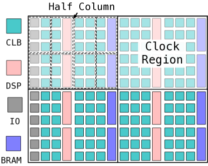
In this work, we use the Xilinx UltraScale family [25, 19],e.g., the UltraScale VU095 as a model FPGA design (illustrated in Fig. 1a). The ISPD 2016 and 2017 FPGA placement challenges employed a condensed version of this architecture with a limited number of instance types, including LUT, FF, BRAM, and DSP [16, 17].
II-A1 SLICEL-SLICEM heterogeneity
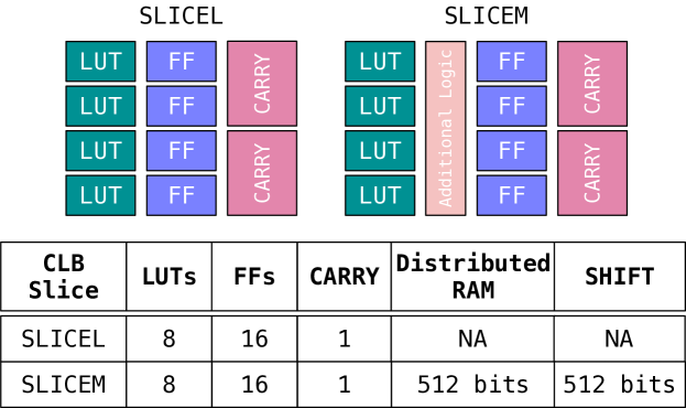
Shift registers (SHIFT) and distributed RAMs are two additional LUT-like instances of the architecture in addition to regular LUTs. Slices in CLBs fall into two categories: SLICEL and SLICEM, whose architectures are depicted in Fig. 1c. Due to the modest differences in logic resources, SLICEL and SLICEM support various configurations. LUTs, FFs, and CARRYs can be placed in both SLICEL and SLICEM. On the other hand, SHIFT and distributed RAMs can only be placed in SLICEM, which sets them apart from other common instances such as DSPs and BRAMs. Additionally, a SLICEM cannot be used as SHIFTs or distributed RAMs if it is configured as LUTs; vice versa.
II-A2 Carry Chain Alignment Constraints
As a placement constraint for CARRY instances, we also need to take carry chain alignment into account. A carry chain is made up of several consecutive CARRY instances connected by cascaded wires from the lower bits to the upper bits, and the CARRY instances are arranged in CLB slices. According to the alignment constraint, each CARRY instance in a chain must be positioned in a single column and in subsequent slices in the correct sequence for the cascading wires.
II-A3 Clock Constraints
The target FPGA device owns rectangular-shaped clock regions (CRs) in a grid manner, as shown in Fig. 1a. 111 Fig. 1a only contains part of the whole CRs, but is sufficient for illustration. . Each CR is made up of columns of site resources and can be further horizontally subdivided into pairs of lower and upper half columns (HCs) of half-clock-region height. Except for a few corner cases, the width of each HC is the same as that of two site columns, as shown in Fig. 1a. All the clock sinks within a half column are driven by the same leaf clock tracks.
The clock routing architecture imposes two clock constraints on placement, i.e., the clock region constraint and the half column constraint, as shown in Fig. 1b. The clock region constraint limits each clock region’s clock demand to a maximum of 24 clock nets, where the clock demand is the total number of clock nets whose bounding boxes intersect with the clock region. The half-column constraint limits the number of clock nets within the half-column to a maximum of 12.
II-B Multi-Electrostatics based FPGA Placement
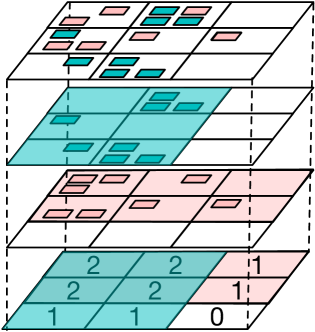
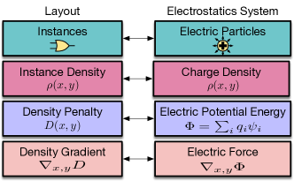
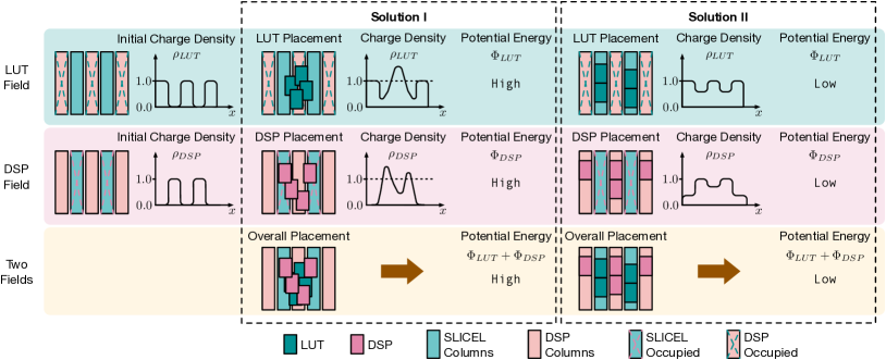
As shown in Fig. 2, electrostatics-based placement models each instance as an electric particle in an electrostatic system. As firstly stated in the ASIC placement [26], minimizing potential energy can resolve density overflow in the layout. The principle is based on the fundamental physical insight that a balanced charge distribution in an electrostatic system contributes to low potential energy, so minimizing potential energy can resolve density overflow and help spread instances in the layout. We are also extending this approach to the use of multiple electrostatic fields, which will enable multiple types of resource to be handled in FPGA placement, such as LUTs, FFs, DSPs, and BRAMs. Fig. 3 illustrates a multi-electrostatic formulation of LUTs and DSPs. In order to reduce density overflow, we must minimize the total potential energy of multiple fields because low energy means a balanced distribution of instances. The issue can be summarized as follows.
| (1) |
where is the wirelength objective, are instance locations, denotes the field type set, and is the electric potential energy for field type . Formally, we constrain the target potential energy of each field type to be zero, though the energy is usually non-negative. The constraints can be further relaxed to the objective and guide the instances to spread out. Practically, we stop the optimization when the energy is small enough; or equivalently, the density overflow is low enough. Notice that the formulation in Fig. 3 assumes that one instance occupies the resources of only one field, which cannot handle the complicated SLICEL-SLICEM heterogeneity shown in Section II-A1.
II-C Timing Optimization
Timing-driven placement imposes more concern about timing closure than the total wirelength objective in wirelength-driven placement. Worst negative slack (WNS) and total negative slack (TNS) are two widely adopted timing metrics. WNS is the maximum negative slack among all timing paths in the design, and TNS is the sum of all negative slacks of timing endpoints. Thus, WNS and TNS are used to evaluate the timing performance of a design from the worst and the global view respectively, and the smaller the WNS and TNS are, the worse the timing performance is. The timing-driven placement problem can be formulated as follows.
| (2a) | ||||
| s.t. | (2b) | |||
where is the instance type set, denotes the density for instance type , and represents the target density for instance type . The objective function can be WNS, TNS, or the weighted sum of both. Improving TNS requires collaborative optimization of all timing paths, and is therefore suitable for the global placement stage. On the other hand, WNS is more suitable for the detailed placement stage, as it only considers the worst timing path. It is worth noting that directly solving Eq. (2) is very difficult, because the delay model generally has strong discrete and non-convex properties [27]. Therefore, we draw on the two intuitive elements of wirelength-driven placement and static timing analysis, i.e., net weights and slacks, to tackle this problem.
II-D Problem Formulation
TABLE I summarizes the characteristics of the published state-of-the-art FPGA placers. In recent years, modern FPGA placers mainly resort to quadratic programming-based approaches [4, 5, 6, 7, 8, 9, 10, 11, 12] and nonlinear optimization-based approaches [13, 14, 15] for the best trade-off between quality and efficiency. Among them, the current state-of-the-art quality is achieved by nonlinear approaches elfPlace [13] and NTUfPlace [15], whose instance density models are derived from a multi-electrostatics system and a hand-crafted bell-shaped field system. However, most existing FPGA placers only consider a simplified FPGA architecture, i.e., LUT, FF, DSP, and BRAM, ignoring the commonplace SLICEL-SLCIEM heterogeneity in real FPGA architectures [5, 6, 7, 8, 13, 9, 10, 11, 14, 15]. Among these placers, only a few placers utilize the parallelism that the GPU provides [13], and few consider timing and clock feasibility in practice [11, 14, 15, 8, 9].
In this work, we aim at optimizing wirelength, timing, and routability while cooperating with SLICEL-SLICEM heterogeneity, alignment feasibility, and clock constraints. We define the FPGA placement problem as follows.
Problem 1 (FPGA Placement).
Taking as input a netlist consisting of LUTs, FFs, DSPs, BRAMs, distributed RAMs, SHIFTs, and CARRYs, generate a plausible FPGA placement solution with optimized wirelength, timings, and routings, satisfying the requirements for alignment feasibility and meeting the clock constraints.
III Algorithms
We will detail the placement algorithm in this section.
III-A Overview of the Proposed Algorithm
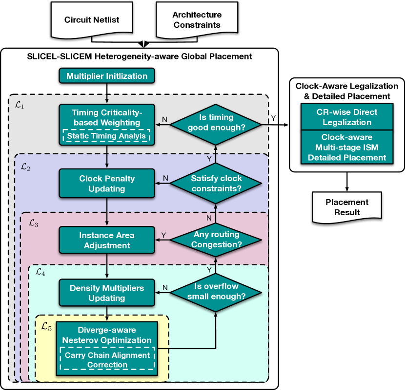
As illustrated in Fig. 4, our method includes two fundamental stages: (1) nested global placement with timing awareness and clock feasibility, and (2) clock-aware legalization and detailed placement.
We cope with the SLICEL-SLICEM heterogeneity by defining the field type set as {LUTL, LUTM-AL, FF, CARRY, DSP, BRAM} with a special field setup (Section III-B). With clock constraints, carry chain alignment feasibility, and timing optimization, we formulate the problem as Formulation (3).
| (3a) | ||||
| s.t. | (3b) | |||
| (3c) | ||||
| Carry chain alignment constraint, | (3d) | |||
is the timing performance objective, where measures the net criticality in the current timing graph (Section III-F). denotes the instance areas in the field , and is the clock penalty term (Section III-E). For brevity, in later discussions, we condense to for all , and denote as the potential energy vector, whose components are the potential energy for each field, i.e., .
We relax the original problem (3) by leveraging the augmented Lagrangian method (ALM) [29] to formulate a better unconstrained subproblem,
| (4a) | ||||
| (4b) | ||||
The density multiplier vector is , and the clock penalty multiplier is . The purpose of the weighting coefficient vector is to achieve a balance between the first-order and second-order terms for density penalty. We follow the setup for and as [13]. To cope with multiple constraints, we rewrite the problem in a nested manner through the Lagrangian relaxation method,
| (5a) | ||||
| (5b) | ||||
| (5c) | ||||
| (5d) | ||||
| (5e) | ||||
where denotes Eq. (4). To put it simply, a set of variables in the objective function is constrained to be the optimal solution of the extra optimization problem, and the variables of the exterior optimization problem are passed toward the sub-problem as fixed parameters. To illustrate, take the solving process of as an example. The subproblem aims at finding the optimal instance positions and given a set of fixed parameters , , , and from . When comes to the convergence to its minimum solution, the optimizer will improve the parameter so as to enlarge the magnitude of the density terms in the overall optimization objectives. Therefore, the optimizer will try to find a better solution by moving the instances to a less dense region in a new iteration, and thus the density constraints will be forced to be gradually adequate. We also adopt the same procedure to solve the other subproblems.
Fig. 4 depicts the nested loops to solve the problem. aims at improving the timing slacks via the timing-criticality-based weighting method. The stopping criterion of is whether timing slacks can be improved (Section III-F). (Section III-E) aims at excluding the cases where clock routing is illegal under an analytical formulation. We regard as converged when there is no clock violation (Section II-A3). develops the area inflation-based technique from [13] in order to optimize the routability, and the estimated routing congestion and pin density are the convergence criteria of . is the core wirelength-driven placement problem. We empirically find that the density overflow is a good indicator of the density constraints. 222 We set the overflow threshold for LUTs and FFs to 10% in our experiments. For , we always solve with a fixed number of iterations, e.g., one iteration in the experiments.
In each iteration, we resolve the carry chain alignment constraints through iterative support from iterative carry chain alignment correction (Section III-D). Following placement, we evolve clock-aware direct legalization and detailed placement algorithms that above clock feasibility constraints are met [8]. We do not include details on routability optimization, clock-aware legalization, or detailed placement for brevity.
III-B Multi-Electrostatic Model for SLICEL-SLICEM Heterogeneity
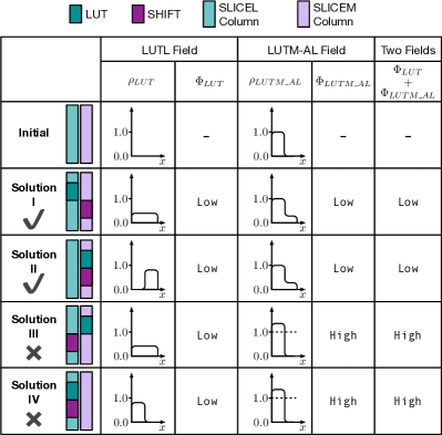
SLICEMs can operate in one of three modes: LUT, distributed RAM, or SHIFT, as discussed in Section II-A1. In the LUT slots of that SLICEM, only instances that match the mode can be placed. In order to address this constraint, we introduce two electrostatic fields, LUTL and LUTM-AL, into the multi-electrostatic placement model. In the field setup, it should be possible to prevent distributed RAM instances or SHIFT instances from being placed on SLICEL sites, however, it should be possible to place LUT instances both on SLICEL and SLICEM sites, as part of the field setup.
There is an example of how these two fields are set up in Fig. 5. LUTL models the LUT resources that are provided by both SLICEM and SLICEL, whereas LUTM-AL models the additional logic resources that are supplied by SLICEM but not by SLICEL. In contrast to a distributed RAM or SHIFT instance, a LUT instance only occupies resources within the LUTL field, while a distributed RAM or SHIFT instance occupies resources both in the LUTL and LUTM-AL fields.
Using an example of a LUT instance and a SHIFT instance as an example, this figure analyses four scenarios. As with SHIFT instances, distributed RAM instances work in exactly the same way. In order to indicate that a SLICEL does not contain any resources for LUTM-AL, we set the initial density for LUTM-AL in a SLICEL to 1, indicating the SLICEL is occupied; in contrast, the initial density for LUTL in a SLICEL is set to 0. We set the initial density of a SLICEM to zero for both LUTL and LUTM-AL due to the fact that it contains both LUTL and LUTM-AL resources. In Solution I, if the LUT instance is placed on a SLICEL and the SHIFT instance is placed on a SLICEM, there will be no overflow of density in either of the fields (a balanced density distribution can be achieved by inserting fillers [26]), which means that the potential energy will be minimized. In Solution II, the scenario is similar to the one in Solution I. Solution III and IV, on the other hand, where the SHIFT instance is placed on a SLICEL, produce a density overflow in the LUTM-AL field, which indicates that there is a high potential energy for this field. As long as the optimizer minimizes the potential energy, these solutions will be avoided. As a result, these two elaborate fields are able to accommodate LUT and distributed RAM/SHIFT to their compatible sites in an easy manner.
III-C Divergence-aware Preconditioning
It is important to precondition the gradient for each iteration before it is fed to the optimizer, where is the Lagrangian problem defined in Eq. (4). A gradient is discussed only in the direction of , and a gradient in the direction of is the same. To make the Jacobi preconditioner more efficient, we approximate the second-order derivatives of wirelength and density according to the following formula.
| (6a) | ||||
| (6b) | ||||
In the above equation, denotes the set of instances, denotes the nets incident to instance , denotes the weight of net , and denotes the second-order derivative of the wirelength term. To optimize the model, we provide the optimizer with the preconditioned gradient .
As shown in Fig. 6, after the loss surfaces have been preconditioned, they are now more isotropic and therefore can be optimized more rapidly. The intuition from the partial derivative itself is that we would expect that for instances with more pins or pins incident to larger net weights, they would move slower than instances with fewer pins, and for instances with larger would also move slower.
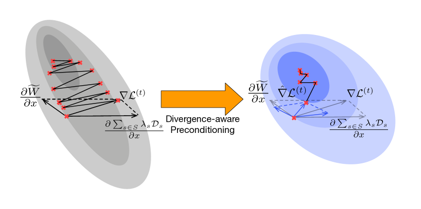
It has been observed that if the ratio of the gradient norms from the density term and the wirelength term becomes too large, the optimization can diverge easily [30, 13]. Thus, we introduce an additional weighting vector , so that we can dynamically control the gradient norm ratio. It is illustrated in Fig. 6 that some instances are dominated by the density gradient, resulting in some instances moving too fast, and this causes the instances to diverge from each other. In most cases, this occurs during the second half of the placement iteration when the density term starts to compete with the wirelength term by increasing to maintain its position in front of it. In order to stabilize the optimization process, we need a new preconditioner. For convenience, we define two auxiliary variables and . Taking the gradient norms of the density and wirelength terms to be equal, we can derive as follows.
| (7a) | ||||
| (7b) | ||||
| (7c) | ||||
denotes the set of instances that have a demand in the field . is the wirelength gradient norm summation of . The weighting vector measures the gradient norm ratio between the density term and the wirelength term, and denotes the average wirelength preconditioner for each field type. The detailed derivations have been omitted for brevity. Experiments will be conducted to further validate its effectiveness.
III-D Iterative Carry Chain Alignment Correction
Using a carry chain alignment technique, we propose a method that can better align the carry chains without affecting the effectiveness of the analytical global placement algorithm. We move the sequential CARRYs together at the end of each global placement iteration, align them based on their horizontal coordinates, and then move them into a column shape at the end of an iteration. The CARRY instances in a chain will move together during the global placement iterations, which eases the legalization step, since the chains will almost align once the global placement process is completed.
III-E Clock Network Planning Algorithm
There is a high degree of dissmoothness in the clock constraints in Section II-A3. The slightest movement within the clock region boundaries can result in an illegal clock configuration, which is detrimental to optimization. In order to simplify the clock planning process, we decompose it into two stages. Our first step is to find an instance-to-clock-region mapping in the first stage. This mapping ensures that all clock region constraints will be satisfied as long as all instances are located within the target clock region during the mapping. The second step involves moving all instances to their target clock regions by adding a penalty term to the placement objective, which is . Following the global placement, the half-column constraints are then dealt with in the developed clock-aware direct legalization and detailed placement algorithm [8]. As we move forward, we will explain these two stages in more detail.
III-E1 Instance-to-Clock-Region Mapping Generation
It is the goal of this step to generate mappings in a manner that ensures that clock constraints can be met with the minimum perturbation to the placement. As discussed in [10], we propose using branch-and-bound method to search through the solution space arising from different instance-to-clock-region mappings, and find a feasible solution with high quality within the solution space. As part of the second stage, we enlist the assignment that has the lowest cost and uses it as a base.
III-E2 The Clock Penalty for Placement
In contrast to [11, 9], which forces instances to move directly to their clock regions, we introduce a bowl-like, smooth, and differentiable gravitational attraction term, which draws instances to the clock regions to which they have been mapped. Let , , , and be the left, right, bottom, and top boundary coordinates of the generated mapping result of instance ’. We define the penalty term for instance as , where is defined as,
| (8) |
A visual representation of the clock penalty term can be found in Fig. 7. in Eq. (3) indicates that the sum of the clock penalty of all instances, i.e., is equal to .
Initially, the clock penalty multiplier is set to a value of 0. As soon as we reset the clock penalty function , we update with the relative ratio between the gradient norms of the wirelength and the clock penalty in order to maintain the stability of the clock penalty function.
| (9) |
As we observe, only 1% of the instances are out of their available clock regions right after they have been assigned the clock region, so most instances have no penalties as a result of this. It is empirically established that is equal to and is equal to as a method of balancing the gradient norm ratio.
III-F Timing-Criticality-based Weighting Method
The timing performance objective (see Eq. (3)) consists of two components: i) the wirelength objective as a first-order approximation of WNS and TNS, and ii) the net criticality that remedies the lack of timing information for first-order approximation.
| (10) |
measures the timing criticality of nets, i.e., whether any timing path through nets violates timing constraints, what is the degree of the violation, and how much the path delay can be reduced. In this section we detail how functions.
III-F1 Static Timing Analysis
Timing-driven placement leverages the static timing analysis (STA) to evaluate the timing criticality of nets. STA relies on (i) model of signal delays for nets and instances, and (ii) a timing analysis engine based on net and instance delays.
Delay models in FPGA are highly coupled with the pre-fabricated routing architecture and the behavior of the FPGA router. In our experiment, we design the linear delay model, where the delay of the routing path between a source endpoint and a sink endpoint is calculated by the Manhattan distance between them. Given the delay of the timing edges, the timing analysis engine determines which timing paths violate their timing constraints. A timing path is a directed acyclic path for particular source and sink pairs (primary I/Os and I/Os of store elements). The delay along a path is the sum of wire delays and cell delays, and every path comes with a timing constraint defined via the actual arrival time (AAT) and required arrival time (RAT) for every driver pin and primary output.
The slack of a path is defined as . We mainly focus on the setup time constraint, which is defined as the difference between the AAT and RAT. A timing path violates the setup time constraints if the slack is negative. The slack of a timing edge is the smallest path slack among the paths containing this edge. To avoid enumerating all paths, we compute the slack from the actual arrival times and required arrival times at timing endpoints [31].
| (11a) | ||||
| (11b) | ||||
In Eq. (11), is an endpoint in the timing graph, and denotes the timing delays from endpoint to endpoint , provided by the delay model. The slack of timing edge connecting the source endpoint and the sink endpoint is
| (12) |
Fig. 8 illustrates the timing analysis process.
III-F2 Timing-driven Net Reweighting Scheme
In the timing graph, nets have diverse effects on the timing slacks. Those nets with higher timing criticality should be more sensitive to the timing closure. To improve the timing in the analytical placement framework, we assign different net weights to different nets based on their timing criticality. Let and denote the timing slacks of net and the worst negative slack, respectively. We define the timing criticality as follows,
| (13) |
where is the clock period. When net is not on a path with timing violation, i.e. , the timing criticality remains zero. Otherwise, the timing criticality equals the ratio . The worse timing slack is, the larger timing criticality it will have. The largest timing criticality falls upon the nets on the most critical path.
After evaluating the timing criticality, we compute the net weight as
| (14a) | ||||
| (14b) | ||||
where is the updated net weight, denotes the reweighting magnitude for net , and is a hyper-parameter that controls the weighting magnitude 333 In our experiments, equals 1. .
III-F3 Effectiveness Analysis of the Rweighting Scheme
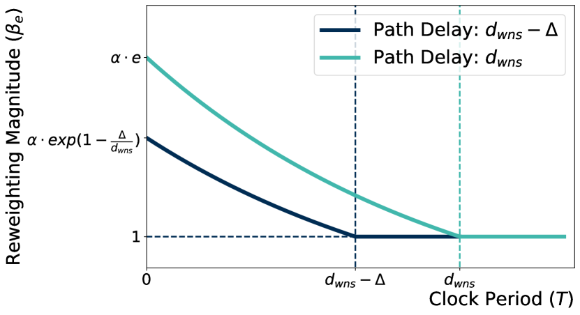
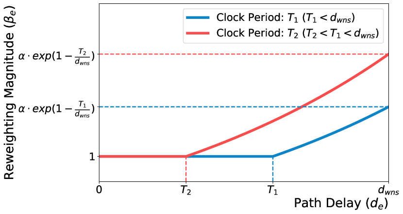
It is suggested that our reweighting scheme can control the reweighting scale according to the severity of the target timing constraints. The reweighting magnitude of a net is determined by the largest magnitude of the timing paths that pass through it, i.e., . We then gave a brief analysis of how the timing path affects the re-weighting scheme in nets.
For the paths with maximal delay , the intuition is that the reweighting method should make no effect, i.e., equals 1, when it has no timing violations. Otherwise, the smaller is, the larger the reweighting magnitude should be. Fig. 9a show the relationship between the magnitude of the reweighting and the clock period for a certain path and its delay. This figure demonstrates that a path will only gain a reweighting magnitude greater than one when the target clock period is less than its path delay. The reweighting magnitude will grow faster with becoming smaller. Fig. 9b regards the path delay as a variable and shows how the reweighting magnitude reacts under a certain clock period. The relationship curves align with our intuition that nets with a smaller timing delay always gain a smaller reweighting magnitude. No matter what the clock period is, the reweighting magnitude only takes effect on those paths with timing violations.
Nets on critical paths gain a larger weighting magnitude in this stage. In the subsequent analytical placement step, the increased net weights then help critical paths tilt more toward timing closure in the tradeoff between timing and area.
IV Experimental Results
We implemented our GPU-accelerated placer in C++ and Python along with the open-source machine learning framework Pytorch for fast gradient back propagation[32]. We conduct experiments on a Ubuntu 18.04 LTS platform that consists of an Intel(R) Xeon(R) Silver 4214 CPU @ 2.20GHz (24 cores), one NVIDIA TITAN GPU, and 251GB memory. We demonstrate the effectiveness and efficiency of our proposed algorithm on both academic benchmarks [17] and industrial benchmarks from the three most concerning aspects of routed wirelength (RWL), runtime (RT), and timing.
IV-A Evaluation on Academic Benchmarks
The statistics of the ISPD 2017 academic benchmark are summarized in TABLE II. The number of instances varies from 400K to 900K with 32–58 clock nets. We do not evaluate the timing performance because on this benchmark we have no access to the timing information of the device. We compare the routed wirelength reported by patched Xilinx Vivado v2016.4 and placement runtime with four state-of-the-art placers, UTPlaceF 2.0 [9], RippleFPGA [11], UTPlaceF 2.X [10], and NTUfplace [15]. All the results of these placers are from their original placers. We do not compare the results with elfPlace because its algorithm cannot handle clock constraints (see TABLE I).
| Design | #LUT/#FF/#BRAM/#DSP | #Clock | UTPlaceF 2.0 [9] | RippleFPGA [11] | UTPlaceF 2.X [10] | NTUfplace [15] | Ours (GPU) | |||||
| RWL | RT | RWL | RT | RWL | RT | RWL | RT | RWL | RT | |||
| CLK-FGPA01 | 211K/324K/164/75 | 32 | 2208 | 532 | 2011 | 288 | 2092 | 180 | 2039 | 698 | 1868 | 136 |
| CLK-FGPA02 | 230K/280K/236/112 | 35 | 2279 | 513 | 2168 | 266 | 2194 | 179 | 2149 | 710 | 2011 | 130 |
| CLK-FGPA03 | 410K/481K/850/395 | 57 | 5353 | 1039 | 5265 | 583 | 5109 | 343 | 4901 | 1704 | 4755 | 215 |
| CLK-FGPA04 | 309K/372K/467/224 | 44 | 3698 | 711 | 3607 | 380 | 3600 | 242 | 3614 | 1148 | 3338 | 162 |
| CLK-FGPA05 | 393K/469K/798/150 | 56 | 4692 | 939 | 4660 | 569 | 4556 | 323 | 4417 | 1540 | 4154 | 208 |
| CLK-FGPA06 | 425K/511K/872/420 | 58 | 5589 | 1066 | 5737 | 591 | 5432 | 346 | 5122 | 2210 | 4918 | 229 |
| CLK-FGPA07 | 254K/309K/313/149 | 38 | 2444 | 845 | 2326 | 304 | 2324 | 201 | 2320 | 795 | 2145 | 141 |
| CLK-FGPA08 | 212K/257K/161/75 | 32 | 1886 | 529 | 1778 | 247 | 1807 | 169 | 1803 | 588 | 1648 | 120 |
| CLK-FGPA09 | 231K/358K/236/112 | 35 | 2601 | 842 | 2530 | 327 | 2507 | 197 | 2436 | 717 | 2248 | 144 |
| CLK-FGPA10 | 327K/506K/542/255 | 47 | 4464 | 974 | 4496 | 512 | 4229 | 286 | 4339 | 1597 | 3839 | 200 |
| CLK-FGPA11 | 300K/468K/454/224 | 44 | 4183 | 1068 | 4190 | 455 | 3936 | 265 | 3964 | 1618 | 3626 | 183 |
| CLK-FGPA12 | 277K/430K/389/187 | 41 | 3369 | 774 | 3388 | 409 | 3236 | 247 | 3179 | 849 | 2938 | 168 |
| CLK-FGPA13 | 339K/405K/570/262 | 47 | 3816 | 1172 | 3833 | 441 | 3723 | 270 | 3680 | 985 | 3404 | 181 |
| Ratio | 1.142 | 4.943 | 1.117 | 2.379 | 1.096 | 1.453 | 1.079 | 6.575 | 1.000 | 1.000 | ||
| Design | #LUT/#FF/#BRAM/#DSP | #Distributed
RAM+#SHIFT |
#CARRY | Clock
Period |
Conference Version [33] | Ours (GPU) | ||||||
| RWL | WNS | TNS | RT | RWL | WNS | TNS | RT | |||||
| IND01 | 17K/11K/0/13 | 9 | 2K | 5 | 90 | -3.941 | -2.422 | 45 | 90 | -1.751 | -1.323 | 70 |
| IND02 | 11K/10K/0/24 | 6 | 335 | 2 | 102 | -4.240 | -19.733 | 54 | 117 | -2.938 | -18.148 | 76 |
| IND03 | 109K/12K/0/0 | 0 | 0 | 3 | 1028 | -2.666 | -18.467 | 59 | 1031 | -2.764 | -16.836 | 144 |
| IND04 | 29K/17K/0/16 | 218 | 1K | 5 | 279 | -5.399 | -27.915 | 83 | 283 | -6.382 | -21.112 | 88 |
| IND05 | 64K/191K/64/928 | 29K | 4K | 10 | 2305 | -10.306 | -3.009 | 97 | 2312 | -4.558 | -2.354 | 218 |
| IND06 | 112K/65K/21/0 | 0 | 4K | 15 | 1585 | -10.987 | -106.384 | 84 | 1585 | -6.502 | -51.922 | 193 |
| IND07 | 40K/156K/89/768 | 26K | 3K | 4 | 1498 | -6.302 | -20.585 | 83 | 1505 | -6.039 | -21.030 | 265 |
| Ratio | 1.000 | 1.000 | 1.000 | 1.000 | 1.025 | 0.764 | 0.775 | 2.029 | ||||
| Design | w/o precond or chain align
(GPU) |
w/o precond
(GPU) |
w/o chain align
(GPU) |
Ours
(GPU) |
||||||||||||
| RWL | WNS | TNS | RT | RWL | WNS | TNS | RT | RWL | WNS | TNS | RT | RWL | WNS | TNS | RT | |
| IND01 | 103 | -3.491 | -2.849 | 53 | 94 | -3.041 | -1.826 | 66 | 108 | -2.581 | -143.009 | 74 | 90 | -1.751 | -1.323 | 70 |
| IND02 | 124 | -4.580 | -28.426 | 148 | 180 | -4.827 | -43.930 | 64 | 118 | -6.449 | -6029.390 | 73 | 117 | -2.938 | -18.148 | 76 |
| IND03 | 1021 | -3.080 | -17.301 | 123 | 1021 | -3.080 | -17.301 | 126 | 1030 | -2.604 | -1776.630 | 125 | 1031 | -2.764 | -16.836 | 144 |
| IND04 | 377 | -9.384 | -28.074 | 88 | 392 | -8.808 | -31.798 | 90 | 290 | -4.288 | -610.918 | 76 | 283 | -6.382 | -21.112 | 88 |
| IND05 | 2290 | -4.502 | -3.702 | 137 | diverge | diverge | diverge | diverge | 2260 | -4.870 | -238.678 | 153 | 2312 | -4.558 | -2.354 | 218 |
| IND06 | 1558 | -50.647 | -105.558 | 109 | 1576 | -11.450 | -113.733 | 107 | 1580 | -15.977 | -5320.100 | 114 | 1585 | -6.502 | -51.922 | 193 |
| IND07 | 1547 | -9.470 | -31.747 | 186 | 1393 | -8.145 | -20.816 | 155 | diverge | diverge | diverge | diverge | 1505 | -6.039 | -21.030 | 265 |
| Ratio | 1.076 | 2.355 | 1.599 | 0.922 | 1.147 | 1.497 | 1.586 | 0.801 | 1.034 | 1.468 | 1.298 | 0.837 | 1.000 | 1.000 | 1.000 | 1.000 |
The experimental results show that our placement algorithm consistently achieves better routed wirelengths than other placers. Specifically, our placer achieves 14.2% smaller routed wirelength than UTPlaceF 2.0, 11.7% smaller than RippleFPGA, 9.6% smaller than UTPlaceF 2.X, and 7.9% smaller than NTUfplace on average, respectively. For some benchmarks, like CLK-FPGA06, which is a large design with about 925K cells and 58 clock nets, our routed wirelength is even 13.6%, 6.7%, 10.5% and 4.1% better than that of baseline placers, respectively. It needs to be mentioned that UTPlaceF 2.X is a follow-up work to UTPlaceF 2.0, which relaxes the clock region bounding box constraints to clock tree constraints. It allows for a larger solution space for clock routing feasibility and thus should yield better results. However, even in this unfair comparison, our routed wirelength is still 9.6% better than UTPlaceF 2.X, exhibiting the efficacy of our algorithm. Besides, our GPU-accelerated placer is the fastest one with 4.94, 2.38, 1.45, and 6.58 speedup over other placers, respectively. These experiments demonstrate the effectiveness and efficiency of our proposed algorithms.
IV-B Evaluation on Industry Benchmarks
We further evaluate our placer on industrial benchmarks which consist of a comprehensive instance set and an industrial FPGA architecture from real-world industry scenarios, including SHIFT, distributed RAM, and CARRY (see TABLE III). Most previous FPGA placers [23, 7, 5, 13, 24, 11, 9, 10, 15, 21] cannot fully handle such an instance set with SLICEL-SLICEM heterogeneity. To better validate the effectiveness of our placer, we leverage a high-quality FPGA router to evaluate the placement algorithms more precisely [34].
From TABLE III, we can see the comparison between the conference version [33] and our placer. Our placer can achieve 23.6% better WNS and 22.5% better TNS, respectively, with minor routed wirelength degeneration, exhibiting the effectiveness of our placer. In some benchmarks, such as IND06, which is one of the most congestion benchmarks, our WNS and TNS are 40.8% and 51.2% better than the baseline, respectively. These experiments demonstrate that our placer can effectively optimize timing even on congested benchmarks. The experiments also show that our placer requires more time to converge on industrial benchmarks. This is because optimizing timing requires additional iterations, which needs further optimization in the future.
IV-C Ablation Study for Optimization Techniques
To better understand the performance of our placer, we perform an ablation study and validate the effectiveness of our proposed methods by disabling optimization techniques as follows (see TABLE IV).
-
•
Disable the iterative carry chain alignment correction in global placement and only align chains once in legalization.
- •
-
•
Disable both techniques as the baseline.
We can see from TABLE IV that both the iterative carry chain alignment correction technique and dynamically-adjusted precondition technique helps stabilizes the global placement convergence and enables better placement solution at convergence. Without either of these two techniques, the placer fails to converge on one design. The dynamically-adjusted preconditioner helps achieve 14.7% better routed wirelength, 49.7% better WNS, and 58.6% better TNS compared with the default preconditioner [13, 30]. Moreover, the iterative carry chain alignment correction helps optimize the routed wirelength, WNS, and TNS by 3.4%, 46.8%, and 29.8% with minor runtime overhead. These experiments validate the effectiveness and efficacy of the proposed carry chain alignment and preconditioning technique.
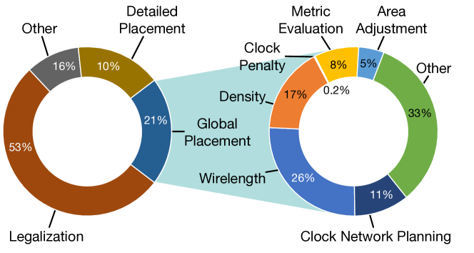
IV-D Runtime Breakdown
To analyze the time consumption of our placer, we further exhibit the runtime breakdown of our algorithm on one of the largest benchmarks as shown in Fig. 10. With the help of GPU acceleration, global placement is no longer the most time-consuming part. The core forward and backward propagation of the global placement, i.e., the computation of wirelength and electrostatic density, as well as their gradients, only take up 26% and 17% of the global placement runtime, respectively. With the great reduction in global placement runtime, legalization becomes the new runtime bottleneck, taking 53% of the total placement time. Meanwhile, other miscellaneous parts, including IOs, parsing, database establishment, etc., take up also the same time as that of global placement.
V Conclusion
In this paper, we present a heterogeneous FPGA placement algorithm that considers the heterogeneity of SLICELs and SLICEMs, as well as timing closure and clock feasibility. A new electrostatic formulation and a nested Lagrangian paradigm have been proposed to achieve uniform optimization of wirelength, routability, timing, and clock feasibility for heterogeneous instance types, including LUT, FF, BRAM, DSP, distributed RAM, SHIFT, and CARRY. Additionally, we propose a dynamically adjusted preconditioner, a timing-driven net-weighting scheme, and a smooth clock penalization technique in order to ensure that the placement is convergent to high-quality solutions. On the ISPD 2017 contest benchmark, experiments have revealed that our placer can achieve 14.2%, 11.7%, 9.6%, and 7.9% better routed wirelengths compared to the state-of-the-art placers, UTPlaceF 2.0, RippleFPGA, UTPlaceF 2.X, and NTUfplace, respectively, at 1.5-6 speedup leveraging GPU acceleration. We conducted experiments on industrial benchmarks to prove that our algorithms are capable of achieving 23.6% better WNS and 22.5% better TNS with about 2% increase in routed wirelength.
References
- [1] S.-J. Lee and K. Raahemifar, “Fpga placement optimization methodology survey,” in Canadian Conference on Electrical and Computer Engineering (CCECE). IEEE, 2008, pp. 001 981–001 986.
- [2] I. L. Markov, J. Hu, and M.-C. Kim, “Progress and challenges in VLSI placement research,” Proceedings of the IEEE, vol. 103, no. 11, pp. 1985–2003, 2015.
- [3] P. Maidee, C. Ababei, and K. Bazargan, “Timing-driven partitioning-based placement for island style fpgas,” IEEE TCAD, vol. 24, no. 3, pp. 395–406, 2005.
- [4] S. Chen and Y. Chang, “Routing-architecture-aware analytical placement for heterogeneous fpgas,” in Proc. DAC. ACM, 2015, pp. 27:1–27:6.
- [5] W. Li, S. Dhar, and D. Z. Pan, “Utplacef: A routability-driven FPGA placer with physical and congestion aware packing,” IEEE TCAD, vol. 37, no. 4, pp. 869–882, 2018.
- [6] C. Pui, G. Chen, W. Chow, K. Lam, J. Kuang, P. Tu, H. Zhang, E. F. Y. Young, and B. Yu, “Ripplefpga: a routability-driven placement for large-scale heterogeneous fpgas,” in Proc. ICCAD, 2016, p. 67.
- [7] R. Pattison, Z. Abuowaimer, S. Areibi, G. Gréwal, and A. Vannelli, “Gplace: a congestion-aware placement tool for ultrascale fpgas,” in Proc. ICCAD, 2016, p. 68.
- [8] W. Li and D. Z. Pan, “A new paradigm for FPGA placement without explicit packing,” IEEE TCAD, vol. 38, no. 11, pp. 2113–2126, 2019.
- [9] W. Li, Y. Lin, M. Li, S. Dhar, and D. Z. Pan, “Utplacef 2.0: A high-performance clock-aware FPGA placement engine,” ACM TODAES, vol. 23, no. 4, pp. 42:1–42:23, 2018.
- [10] W. Li, M. E. Dehkordi, S. Yang, and D. Z. Pan, “Simultaneous placement and clock tree construction for modern fpgas,” in Proc. FPGA, 2019, pp. 132–141.
- [11] C. Pui, G. Chen, Y. Ma, E. F. Y. Young, and B. Yu, “Clock-aware ultrascale FPGA placement with machine learning routability prediction: (invited paper),” in Proc. ICCAD. IEEE, 2017, pp. 929–936.
- [12] T. Liang, G. Chen, J. Zhao, L. Feng, S. Sinha, and W. Zhang, “Amf-placer: High-performance analytical mixed-size placer for fpga,” in Proc. ICCAD, 2021, pp. 1–6.
- [13] Y. Meng, W. Li, Y. Lin, and D. Z. Pan, “elfplace: Electrostatics-based placement for large-scale heterogeneous fpgas,” IEEE TCAD, 2021.
- [14] Y. Kuo, C. Huang, S. Chen, C. Chiang, Y. Chang, and S. Kuo, “Clock-aware placement for large-scale heterogeneous fpgas,” in Proc. ICCAD, 2017, pp. 519–526.
- [15] J. Chen, Z. Lin, Y. Kuo, C. Huang, Y. Chang, S. Chen, C. Chiang, and S. Kuo, “Clock-aware placement for large-scale heterogeneous fpgas,” IEEE TCAD, vol. 39, no. 12, pp. 5042–5055, 2020.
- [16] S. Yang, A. Gayasen, C. Mulpuri, S. Reddy, and R. Aggarwal, “Routability-driven FPGA placement contest,” in Proc. ISPD, 2016, pp. 139–143.
- [17] S. Yang, C. Mulpuri, S. Reddy, M. Kalase, S. Dasasathyan, M. E. Dehkordi, M. Tom, and R. Aggarwal, “Clock-aware FPGA placement contest,” in Proc. ISPD, 2017, pp. 159–164.
- [18] M.-C. Kim, N. Viswanathan, Z. Li, and C. Alpert, “ICCAD-2013 CAD contest in placement finishing and benchmark suite,” in Proc. ICCAD, 2013, pp. 268–270.
- [19] Ultrascale architecture clb slices. [Online]. Available: https://www.xilinx.com/support/documentation/user_guides/ug574-ultrascale-clb.pdf
- [20] T. Martin, D. Maarouf, Z. Abuowaimer, A. Alhyari, G. Gréwal, and S. Areibi, “A flat timing-driven placement flow for modern fpgas,” in Proc. DAC. ACM, 2019, p. 4.
- [21] Z. Lin, Y. Xie, G. Qian, J. Chen, S. Wang, J. Yu, and Y.-W. Chang, “Timing-driven placement for fpgas with heterogeneous architectures and clock constraints,” in Proc. DATE. IEEE, 2021, pp. 1564–1569.
- [22] A. Marquardt, V. Betz, and J. Rose, “Timing-driven placement for fpgas,” in Proc. FPGA. ACM, 2000, pp. 203–213.
- [23] G. Chen, C.-W. Pui, W.-K. Chow, K.-C. Lam, J. Kuang, E. F. Young, and B. Yu, “RippleFPGA: Routability-driven simultaneous packing and placement for modern FPGAs,” IEEE TCAD, vol. 37, no. 10, pp. 2022–2035, 2018.
- [24] Z. Abuowaimer, D. Maarouf, T. Martin, J. Foxcroft, G. Gréwal, S. Areibi, and A. Vannelli, “GPlace3.0: Routability-driven analytic placer for UltraScale FPGA architectures,” ACM TODAES, vol. 23, no. 5, pp. 66:1–66:33, 2018.
- [25] Ultrascale architecture clocking resources. [Online]. Available: https://www.xilinx.com/support/documentation/user_guides/ug572-ultrascale-clocking.pdf
- [26] J. Lu, P. Chen, C.-C. Chang, L. Sha, D. J.-H. Huang, C.-C. Teng, and C.-K. Cheng, “ePlace: Electrostatics-based placement using fast fourier transform and nesterov’s method,” ACM TODAES, vol. 20, no. 2, p. 17, 2015.
- [27] A. B. Kahng, S. Mantik, and I. L. Markov, “Min-max placement for large-scale timing optimization,” in Proc. ISPD, 2002, pp. 143–148.
- [28] J. Lu, H. Zhuang, P. Chen, H. Chang, C.-C. Chang, Y.-C. Wong, L. Sha, D. Huang, Y. Luo, C.-C. Teng et al., “ePlace-MS: Electrostatics-based placement for mixed-size circuits,” IEEE TCAD, vol. 34, no. 5, pp. 685–698, 2015.
- [29] R. Andreani, E. G. Birgin, J. M. Martínez, and M. L. Schuverdt, “On augmented lagrangian methods with general lower-level constraints,” SIAM Journal on Optimization, vol. 18, no. 4, pp. 1286–1309, 2008.
- [30] C.-K. Cheng, A. B. Kahng, I. Kang, and L. Wang, “Replace: Advancing solution quality and routability validation in global placement,” IEEE TCAD, 2018.
- [31] T. Huang and M. D. F. Wong, “Opentimer: A high-performance timing analysis tool,” in Proc. ICCAD. IEEE, 2015, pp. 895–902.
- [32] Y. Lin, Z. Jiang, J. Gu, W. Li, S. Dhar, H. Ren, B. Khailany, and D. Z. Pan, “DREAMPlace: Deep learning toolkit-enabled gpu acceleration for modern vlsi placement,” IEEE TCAD, June 2020.
- [33] J. Mai, Y. Meng, Z. Di, and Y. Lin, “Multi-electrostatic fpga placement considering slicel-slicem heterogeneity and clock feasibility,” in Proc. DAC, 2022, pp. 649–654.
- [34] J. Wang, J. Mai, Z. Di, and Y. Lin, “A robust fpga router with concurrent intra-clb rerouting,” in Proc. ASPDAC, 2023, pp. 529–534.