Effect of electron thermal conductivity on resonant plasmonic detection in the metal/black-AsP/graphene FET terahertz hot-electron bolometers
Abstract
We analyze the two-dimensional electron gas (2DEG) heating by the incident terahertz (THz) radiation in the field-effect transistor (FET) structures with the graphene channels (GCs) and the black-phosphorus and black-arsenic gate barrier layers (BLs). Such GC-FETs can operate as bolometric THz detectors using the thermionic emission of the hot electrons from the GC via the BL into the gate. Due to the excitation of plasmonic oscillations in the GC by the THz signals, the GC-FET detector response can be pronouncedly resonant, leading to elevated values of the detector responsivity. The lateral thermal conductivity of the 2DEG can markedly affect the GC-FET responsivity, in particular, its spectral characteristics. This effect should be considered for the optimization of the GC-FET detectors.
I Introduction
The field-effect transistor (FET) structures with the graphene channel (GC) and the gate barrier layer (BL) made of the black-Phosphorus (b-P), black-Arsenic (b-As), and the compounds of these materials (b-As1-xPx) have shown promise for various device applications. This is because of the unique electron properties of GCs [1] and the b-As1-xPx layers [2, 3] (predicted and demonstrated a long time ago [4, 5]). Changing the As mole fraction and the BL thickness [6, 7, 8] allows to achieve a desirable band alignment and the height of the barriers between GC and the gate, therefore controlling the thermionic activation energy. The latter opens up additional prospects for the FET’s optimization and use for novel devices, in particular, photodetectors[9, 10, 11, 12, 13, 14, 15, 16, 17, 18, 19, 20, 21]. Recently [22], we proposed and evaluated the hot-electron bolometric detector of terahertz radiation (THz) based on such FET structures. Our analysis confirmed the controllability of the electron activation energy by doping and the gate bias voltage and predicted high values of the detector responsivity associated with the effective heating of the two-dimensional electron gas (2DEG) in the GC by the signal electric field produced by the impinging THz radiation, especially when the plasmonic oscillations are resonantly excited.
In this paper, we generalize the device model of GC-FET detectors with b-P and b-As
BLs by accounting for the following effects:
(1) the electron thermal conductance along the GC and
(2) the electron cooling due to the thermionic emission from the GC into the gate (the Peltier cooling).
The role of the electron thermal conductivity can be crucial since it is fairly high (see, for example, [23, 24]).
Thermionic cooling
can become essential at elevated gate bias voltages when the effective
height of the energy barrier for electrons (holes) decreases.
These effects can influence the detector’s performance and should be taken into account for its optimization.
II Device structure
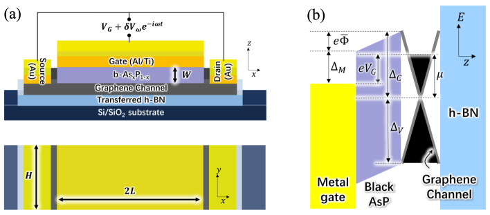
Figure 1 shows the GC-FET structure cross-section and top view and its band diagram when the gate bias voltage . For the definiteness, the materials for the BL and the metal gate, and the GC doping are chosen to provide the flat band in the BL at . This band diagram configuration corresponds to the Ohmic side contacts (the FET source and drain). In particular, we focus on the GC-FETs with the b-P and b-As BLs and Al and Ti gates (the Al/b-P/GC and Ti/b-As/GC devices). The GC and the gate length (the spacing between the side contacts, their width, and the thickness of the BL are set to be , , and , respectively (with ). We focus on the GC-FETs with the GC doped by donors. We assume that the activation energy for the electrons in the GC , where and are the band offsets between the BL conduction and valence bands and the Dirac point in the GC, and is the difference between the BL and the GC work functions. Here is the electron Fermi energy in the GC at , which is determined by the donor density . The latter inequality implies that the thermionic electron gate current dominates over the hole current. The GC-FET devices in which the above condition is not valid can be considered analogously.
The voltage between the GC side contacts and the highly conducting metal gate comprises, apart from the bias voltage , the ac component , where and are the signal amplitude and the frequency. This is the signal generated in an antenna by incident THz radiation. The THz signal could excite the plasmonic oscillation modes with the symmetric spatial distribution of the ac potential in the GC.
III 2DEG heating
The variation of the thermionic gate current, , associated with the incoming THz signal is given by
| (1) |
where is the maximal value of the current density from the GC, which we estimate as with and being the 2DEG density in the GC and the escape time, respectively, of the electrons with the energy exceeding the barrier height. Both and depend on doping and the gate bias voltage.
The quantity comprises the ac component and the rectified dc component (as well as the second and higher harmonics). The latter is the variation of the current density averaged over the period of the THz signal . According to Eq. (1), the rectified component can be presented as
| (2) |
where
| (3) |
The dependence of the factor on the gate voltage is associated with the voltage dependence of the electron Fermi energy (see below).
The variation of the local averaged 2DEG temperature, is governed by the following electron heat transport equation:
| (4) |
Here is the electron thermal conductivity in the GC per electron (this corresponds to the Wiedemann-Franz relation), is the electron energy relaxation time in the GC, cm/s is the characteristic electron velocity in GCs, and is the electron scattering frequency in the GC. The second term in the left side of Eq. (4) is associated with the 2DEG energy transfer to the phonon system (particularly to optical phonons), while the terms in the right site, and , are the Joule power received by the 2DEG in the GC and the power transferred by the electrons emitted from the 2DEG over the BL averaged over time (see, for example, [25]). The Joule contribution to the 2DEG heating is given by
| (5) |
Here, accounting for the excitation of plasmonic oscillations in the gated 2DEG (see, for example, [26, 27, 28, 29, 30, 31, 32, 33, 34, 35, 36] and the references therein) by the THz signal received by an antenna, one can obtain for the ac potential in the GC [22]
| (6) |
Hence for the square of the signal electric field amplitude we arrive at
| (7) |
where Re , and are the Drude dc conductivity and the electron scattering frequency in the 2DEG, and are the effective wavenumber and the plasmonic frequency (corresponding to the symmetric conditions at the contacts), respectively, with and being the dielectric constant of the BL and its thickness. The quantity , which characterizes the cooling of the 2DEG, is presented as
| (8) |
IV Rectified current
Assuming sufficiently low thermal resistance of the highly conducting side contacts, we set the following boundary conditions for Eq. (4):
| (9) |
Solving Eq. (4) with the boundary conditions given by Eq. (9) and invoking Eq. (2), we arrive at the following spatial distribution of the rectified current density:
| (10) |
where is the ”thermal” length. The spatial dependence in the right-hand side of Eq. (10) reflects the nonuniformity of the 2DEG heating associated with the nonuniform distribution of the ac plasmonic electric field along the GC.
The rectified current density is an oscillatory function of the signal frequency. It exhibits the resonant peaks at , where is the index of the plasmonic resonance, provided that . The latter inequality is assumed in the following.
Considering the condition , Eq. (10) can be somewhat simplified and presented as
| (11) |
Introducing the parameter and solving Eq. (10) with boundary conditions (9), we obtain
| (12) |
Integrating , given by Eq. (12), over the GC plane, for the net rectified current at the plasmonic resonances, we arrive at the following expression:
| (13) |
Here
| (14) |
The factor characterizes the effect of the electron thermal conductivity on the rectified current and the signal frequency dependence of the latter.
V GC-FET Detector responsivity.
The current responsivity (in the units A/W) of the GC-FET detector is proportional to the net rectified current , which is given by Eqs. (13) and (14), divided the incident THz radiation power collected by an antenna. Considering that the relation between the ac voltage generated at the side contacts and the power [36] is given by (with being the speed of light in vacuum), we obtain the GC-FET bolometric detector responsivity
| (15) |
Here
| (16) |
where we assumed that the antenna gain [37] and took into account that the fine structure parameter . To account for the effect of the 2DEG viscosity on the plasma oscillations damping in Eq. (15), we set [38] , where and are related to the electron interaction with impurities and acoustic phonons and the electron viscosity of the 2DEG in the GC, respectively.
Using Eq. (16), for room temperature
for meV and m,
we obtain the estimate Eq. (16) yields A/W.
VI Spectral characteristics
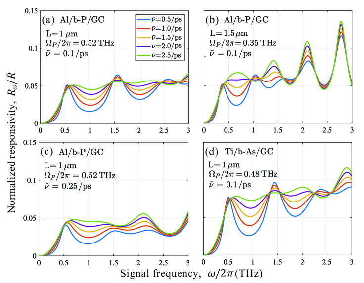
Below we calculate the room temperature GC-FET detector responsivity as a function of the signal frequency for different plasmonic and collision frequencies and bias voltages using Eqs. (15) and (16) and invoking Eq. (14). As examples, we consider the GC-FETs with the band parameters listed in Table I. Other parameters are indicated in the figure captures.
| Structure | (meV) | (meV) | (meV) | (meV) |
|---|---|---|---|---|
| Al/b-P/GC | 85 | 125 | 225 | 140 |
| Ti/b-As/GC | 70 | 90 | 190 | 120 |
Figure 2 shows the spectral dependences of the normalized responsivity of the GC-FET bolometric detectors with the Al/b-P/GC and Ti/b-As/GC structures calculated for different values of the frequencies and (and, hence, different electron thermal lengths) and different GC lengths at meV and . The latter implies that . The structural parameter ranges are discussed below in Appendix A.
The frequency dependences of the responsivity demonstrated in Figs. 2 and 3 exhibit the pronounced peaks at the frequencies close to the plasmonic resonant frequencies . As follows from the comparison of Figs. 2(a) and 2(c), an increase in the electron viscosity markedly smears the higher plasmonic resonances.
One can see from Fig. 2 that the responsivity can be markedly smaller than its characteristic value , even at the resonant maxima (about one order of magnitude smaller as follows, for example, from Eq. (17) and the consequent estimate).
VII Role of electron thermal conductivity
An increase in the collision frequency leads, as might be expected, to a smearing of the resonant peaks. However, the average values of the responsivity show a moderate increase with increasing . This can be interpreted by a smaller electron thermal conductivity in the GCs with a larger . As a result, increasing collision frequency gives rise to a smaller Joule power but a weaker transfer of the 2DEG heat to the side contacts. The comparison of Figs. 2(a) and 2(b) indicates that in the devices with a longer GC, the peaks corresponding to higher resonances can be much more pronounced. This is because an increase in leads to a weakening of the electron thermal transfer (the parameter ).
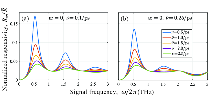
To confirm the significance of the electron thermal transfer in the GC-FETs under consideration, we calculated the frequency dependences of the responsivity disregarding the electron thermal conductivity, i.e., neglecting the electron heat transfer to the side contacts. Figure 3 shows the responsivity of the GC-FET with the parameters used for Figs. 2(a) and 2(c) calculated for the hypothetical case when the electron thermal conductivity is insignificant. One can see that in the case of , the resonant peaks are higher and their smearing is weaker. The plots of Fig. 3 are similar to those in [22] (despite a marked difference in the electron viscosity strength). Thus, the electron thermal transfer along the GC to the side contacts pronouncedly affects the responsivity spectral characteristics. The comparison of the plots in Fig. 3(a) and 3(b) indicates that the electron viscosity naturally weakens the plasmonic resonances.
VIII Comments
An increase in the gate voltage results in the rise of associated with a larger factor in some range of larger voltages (see Appendices A and B). Considering Eq. (3) and accounting for Eq. (B3), for not too large , we obtain
| (17) |
Here (see Appendices A and B). As follows from Eq. (17), the sensitivity of the factor to the gate voltage is weakened by a relatively small parameter .
In the expression for the signal current density given by Eq. (2), we disregarded the rectified component associated with the modulation of the activation energy by the plasmonic oscillations potential. The thermionic current density as a function of the net voltage drop is determined by by the following factor: , where is given by Eq. (6). At low gate voltage, the pertinent ac current density component is equal to
| (18) |
Comparing the thermionic rectified current density given by Eq. (2) and the consequent formulas with , described by Eq. (18), at the pronounced plasmonic resonances (), we obtain
| (19) |
Since the factors and in the right-hand side of Eq. (19) are much larger than unity, .
Apart from the detector responsivity analyzed above, the responsivity, , normalized by the detector area can be used. For one can obtain , where is the antenna aperture [36] and is the wavelength of the incident radiation in vacuum. This implies that , at least in the THz range, and , hence and exhibit fairly different spectral characteristics.
Using Eqs. (14) and (18), we find that reaches a maximum at . Setting, for example, meV, meV, and meV, we obtain meV. However, it is impractical to use such large gate voltages because this can lead to very high DC density [given by Eq. (B4)], at which the spatial distribution of the steady-state temperature of the 2DEG can be substantially nonuniform, particularly, when the current-crowding effect might become crucial. Moreover, at the voltages in question, the electron tunneling between the GC and the gate can enable an elevated tunneling current (see Appendix C). Although the tunneling current does not markedly affect the bolometric response (due to its weak dependence on the 2DEG effective temperature), it together with the elevated thermionic current can substantially decrease the GC-FET detector dark-current limited detectivity.
This implies that the maximal GC-FET detector detectivity can be achieved at small when the dark current density is fairly small, being primarily limited not by the dark current but by the Johnson-Nyquist noise (see, for example, [42]).
Conclusions
We evaluate the effect of the electron thermal conductivity on the characteristics of the GC-FET bolometric THz detectors with the Al/b-P/GC and Ti/b-As/GC. The operation of such devices is enabled by the heating of the 2DEG in the GC by the THz radiation resulting in an increase in the thermionic current from the GC via the b-P or b-As BLs into a metal gate. We demonstrate that the electron thermal conductivity in the GC can markedly influence the 2DEG energy balance pronouncedly affecting the value and the spectral characteristics of the GC-FET detectors, which should be accounted for in the device optimization.
Author’s contributions
All authors contributed equally to this work.
Acknowledgments
The Japan Society for Promotion of Science (KAKENHI Grants 21H04546 and 20K20349), Japan; RIEC Nation-Wide Collaborative Research Project R04/A10; the US Office of Scientific, Research Contract N00001435, (Project Monitor Dr. Ken Goretta).
Data availability
The data that support the findings of this study are available within the article.
Appendix A. Device parameters
We assume that the electron energy relaxation time at room temperature is determined primarily by the GC optical phonons [43, 44, 45, 46, 47] and the interface optical phonons [48, 49]. The analysis of these references, considering that the time of the spontaneous optical phonon emission in GC ps and accounting for the smallness of the optical phonon number at room temperature, leads to the estimate ps. The escape of an electron with an energy exceeding from 2DEG into the gate via the BL is possible after its scattering on acoustic phonons and impurities with a substantial variation of the electron momenta (with the electron turning almost perpendicular to the GC plane). Assuming that the electron momentum relaxation time associated with the acoustic phonon scattering at room temperature ps [50, 51, 52], one can conclude that or even . Considering this, in our estimates and calculations below, we set ps.
The voltage factor in Eqs. (9) - (12) depends on the bias voltage , which affects the electron Fermi energy . At moderate bias voltages, the versus is given by Eq. (3) with , where with cm/s being the characteristic electron velocity in GCs. If and nm, one obtains meV. At low bias voltages . Considering the GC-FET Al/b-P/GC structures with meV and the Ti/b-As/GC structures with meV, for room temperature we obtain and , respectively.
We estimate the electron thermal conductivity as . For ps-1, the latter yields cm2/s. These values are smaller than the record electron thermal conductivity, which can be extracted from the experimental papers [23, 24] for the 2DEG in the suspended GCs with the electron densities cm-1. The lower values assumed by us can be justified by the presence of the gate layer and the substrate surrounding the GC in the devices under consideration. Thus, the thermal length (at a small )
| (A1) |
depends on the quality of the GC and the interfaces between the GS and the surrounding layers (via the dependence on ) and on the contribution of the surface optical phonons to the electron energy relaxation time (via the dependence on ). This implies that the value of can vary in a wide range. For definiteness, we fix and , calculating the GC-FET detector characteristics for different .
Setting ps, ps, , and ps-1, we find m.
The quantity , where cm2/s [38] is the electron viscosity coefficient and is the wavenumber of the plasma mode in the GC-FET under consideration. For the above values of and m, one obtains ps-1.
Appendix B. Fermi energy vs gate voltage
When the electron plasma in the GC is degenerate () is governed by the following equation:
| (B1) |
where the term proportional to corresponds to the electron density electrically induced in the GC (its dependence on reflects the quantum capacitance effect [53, 54, 55]). Under the condition of the BL flat band at , hence , and . Considering this, we arrive at
| (B2) |
with .
For moderate and high gate voltages Eq. (B2) yields
| (B3) |
respectively.
In particular, using Eqs. (2) and (B3), for the dc current-voltage characteristics in the most actual range of moderate gate voltages, we obtain:
| (B4) |
Appendix C. Tunneling
At sufficiently high gate voltages when , the energy barrier in the BL can become triangular, where and The latter inequality yields .
In this case, the electron tunneling from the GC into the gate (via the triangular barrier in question) can be substantial.
The tunneling electron current through the triangular potential barrier assumed above [see Fig. 1(b)], can be estimated as [56]
| (C1) |
where is the electron effective mass in the BL.
Accounting for Eqs. (2)and (B4), for the net DC current at large gate voltages we obtain
| (C2) |
Considering that a , Eq. (C2) becomes
| (C3) |
Hence, the thermionic current exceeds the tunneling current if
| (C4) |
Accounting for that the responsivity maximum corresponds to , we obtain
| (C5) |
Assuming g and nm for room temperature we find V.
In devices with relatively large (in which even at the energy barrier in the BL is triangular, i.e., at ), the quantity can be small even at high bias voltages , so that might be fairly large.
References
- [1] A. H. Castro Neto, F. Guinea, N. M. Peres, K. S. Novoselov, and A. K. Geim, “The electronic properties of graphene,” Rev. Mod. Phys. 81, 109 (2009).
- [2] Xi Ling, H. Wang, S. Huang, F. Xia, and M. S. Dresselhaus, “The renaissance of black phosphorus,” PNAS 122, 4523 (2015).
- [3] F. Xia, H. Wang, and Y. Jia, “Rediscovering black phosphorous as an anisotropic layered material for optoelectronics and electronics,” Nat. Commun. 5, 4458 (2014).
- [4] R. W. Keyes, “The electrical properties of black phosphorus,” Phys. Rev. 92, 580 (1953).
- [5] H. Asahina and A. Morita, “Band structure and optical properties of black phosphorus,” J. Phys. C: Solid State Phys. 17 1839 (1984).
- [6] Y. Cai, G. Zhang, and Y.-W. Zhang, “Layer-dependent band alignment and work function of few-layer phosphorene,” Sci. Rep. 4, 6677 (2015).
- [7] B. Liu, M. Kopf, A. N. Abbas, X. Wang, Q. Guo, Y. Jia, F. Xia, R. Weihrich, F. Bachhuber, F. Pielnhofer, H. Wang, R. Dhall, S. B. Cronin, M. Ge, X. Fang, T. Nilges, and C. Zhou, “Black Arsenic-Phosphorus: layered anisotropic infrared semiconductors with highly tunable compositions and properties,” Adv. Mater. 27, 4423 (2015).
- [8] T. Hu, B. Xu, and J. Hong, “Two-dimensional As1-xPx binary compounds: Highly tunable electronic structure and optical properties,” Current Appl. Phys. 17, 186 (2017).
- [9] Z. Guo, H. Zhang, S. Lu, Z. Wang, S. Tang, J. Shao, Z. Sun, H. Xie, H. Wang, X.-F. Yu, and P. K. Chu, “From black phosphorus to phosphorene: Basic solvent exfoliation, evolution of Raman scattering, and applications to ultrafast photonics,” Adv. Funct. Mater. 25, 6996 (2015).
- [10] M. Xie, S. Zhang, Bo Cai, Y. Huang, Y. Zou, B. Guo, Yu Gua, and H. Zeng, “A promising two-dimensional solarcell donor: Black arsenic–phosphorus monolayer with 1.54 eV directband gap and mobility exceeding 14,000cm2Vs,” Nano Energy 28, 433 (2016).
- [11] M. Long, A. Gao, P. Wang, H. Xia, C. Ott, C. Pan, Y. Fu, E. Liu, X. Chen, W. Lu, T. Nilges, J. Xu, X. Wang, W. Hu, and F. Miao, “Room temperature high-detectivity mid-infrared photodetectors based on black arsenic phosphorus,” Sci. Adv. 3, e1700589 (2017).
- [12] V. Ryzhii, T. Otsuji, M. Ryzhii, D. S. Ponomarev, V. E. Karasik, V. G. Leiman, V. Mitin, and M. S. Shur, “Electrical modulation of terahertz radiation using graphene-phosphorene heterostructures,” Semicond. Sci. Technol. 33, 124010 (2018).
- [13] V. Ryzhii, M. Ryzhii, D. Svintsov, V. Leiman, P. P. Maltsev, D. S. Ponomarev, V. Mitin, M. S. Shur, and T. Otsuji,“Real-space-transfer mechanism of negative differential conductivity in gated graphene-phosphorene hybrid structures: Phenomenological heating model,” J. Appl. Phys. 124, 114501 (2018).
- [14] V. Ryzhii, T. Otsuji, M. Ryzhii, A. A. Dubinov, V. Ya. Aleshkin, V. E. Karasik, and M. S. Shur, “Negative terahertz conductivity and amplification of surface plasmons in graphene–black phosphorus injection laser heterostructures,” Phys. Rev. B 100, 115436 (2019).
- [15] T. Liu,, L. Tong, X. Huang, and L. Ye, “Room-temperature infrared photodetectors with hybrid structure based on two-dimensional materials,” Chin. Phys. B 28, 017302 (2019).
- [16] A. Gao, Z. Zhang, L. Li, B. Zheng, C. Wang, Y. Wang, T. Cao, Yu Wang, S.-J. Liang, F. Miao, Yi Shi, and X. Wang, “Robust impact-ionization field-effect transistor based on nanoscale vertical Graphene/Black Phosphorus/Indium Selenide heterostructures,” ACS Nano 14, 434 (2020).
- [17] V. Ryzhii, M. Ryzhii V. G. Leiman, V. E. Karasik, V. Mitin, M. S. Shur, and T. Otsuji, “Far-infrared photodetectors based on nanoribbon heterostructures with black-AsP barrier layers,” Opt. Exp. 28, 2480 (2020).
- [18] X.-Q. Jiang, X.-K. Li, Sh.-N. Chen, B.-W. Su, K.-X. Huang, Z.-Bo Liu, and J.-G. Tian, “Tunneling devices based on graphene/ black phosphorus van der Waals heterostructures,” Mat. Res. Exp. 7, 016310 (2020)
- [19] A. Parappurath, S. Mitra, G. Singh, N. K. Gill, T. Ahmed, T. P. Sai, K. Watanabe, T. Taniguchi, and A.Ghosh, “Interlayer charge transfer and photodetection efficiency of graphene–transition-metal-dichalcogenide heterostructures,” Phys. Rev. Appl. 17, 064062 (2022).
- [20] R. Han, S. Feng, D.-M. Sun, and H.-M. Cheng, “Properties and photodetector applications of two-dimensional black arsenic phosphorus and black phosphorus,” Science China 64, 140402 (2021).
- [21] L. Wu, T. Fan, S. Wei, Y. Xu, Ye Zhang, et al., “All-optical logic devices based on black arsenic–phosphorus with strong nonlinear optical response and high stability,” Opto-Electron Adv. 5, 200046 (2022).
- [22] V. Ryzhii, C. Tang, T. Otsuji, M. Ryzhii, V. Mitin, and M. S. Shur, “Resonant plasmonic detection of terahertz radiation in field-effect transistors with the graphene channel and the black-AsxP1-x gate layers: Hot carrier bolometric mechanism,” Sci. Rep. (2023), submitted.
- [23] Z. Tong, A. Pecchia, C. Yam, T. Dumitrică, and T. Frauenheim “Ultrahigh electron thermal conductivity in T-Graphene, Biphenylene, and Net-Graphene,” Adv. Energy Mater. 12, 2200657 (2022)
- [24] T. Y. Kim, C.-H. Park, and N. Marzari,“The electronic thermal conductivity of graphene,” Nano Lett. 16, 2439 (2016).
- [25] J. F. Rodriguez-Nieva, M. S. Dresselhaus, L. S. Levitov, “Thermionic emission and negative dI/dV in photoactive graphene heterostructures,” Nano Lett., 15 145 (2015).
- [26] V. Ryzhii, “Terahertz plasma waves in gated graphene heterostructures,” Jpn. J. Appl. Phys. 45, L923 (2006).
- [27] V. Ryzhii, A. Satou, and T. Otsuji, “Plasma waves in two-dimensional electron-hole system in gated graphene heterostructures,” J. Appl. Phys. 101, 024509 (2007).
- [28] A. N. Grigorenko, M. Polini, and K. S. Novoselov, “Graphene plasmonics,” Nat. Photonics 6, 749 (2012).
- [29] A.V. Muraviev, S. L. Rumyantsev, G. Liu, A. A. Balandin, W. Knap, and M. S. Shur, “Plasmonic and bolometric terahertz detection by graphene field-effect transistor,” Appl. Phys. Lett. 103, 181114 (2013).
- [30] O.V. Polischuk, D. V. Fateev, T. Otsuji, and V. V. Popov, “Plasmonic amplification of terahertz radiation in a periodic graphene structure with the carrier injection,” Appl. Phys. Lett. 111, 081110 (2017).
- [31] T. Low and P. Avouris, “Graphene plasmonics for terahertz to mid-infrared applications,” ACS Nano. 8, 1086 (2014).
- [32] V. Ryzhii, T. Otsuji, M. Ryzhii, V. Mitin, and M. S. Shur, “Resonant plasmonic terahertz detection in vertical graphene-base hot-electron transistors,” J. Appl. Phys. 118, 204501 (2015).
- [33] T. J. Constant, S. M. Hornett, D. E. Chang, and E. Hendry, “All-optical generation of surface plasmons in graphene,” Nat. Phys. 12, 124 (2016).
- [34] O.V. Polischuk, D. V. Fateev, T. Otsuji, and V. V. Popov, “Plasmonic amplification of terahertz radiation in a periodic graphene structure with the carrier injection,”Appl. Phys. Lett. 111, 081110 (2017).
- [35] D. A. Bandurin, D. Svintsov, I. Gayduchenko, G. Shuigang, G. Xu, A. Principi, M. Moskotin, I. Tretyakov, D. Yagodkin, S. Zhukov, T. Taniguchi, K. Watanabe, I. V. Grigorieva, M. Polini, G. N. Goltsman, A. K. Geim, and G. Fedorov, “Resonant terahertz detection using graphene plasmons,” Nat. Commun. 9, 5392 (2018).
- [36] V. Ryzhii, T. Otsuji, and M. S. Shur, “Graphene based plasma-wave devices for terahertz applications,” Appl. Phys. Lett. 116, 140501 (2019).
- [37] R. E. Colin Antenna and Radiowave Propagation (New York, McGraw-Hill, 1985).
- [38] Y. Zhang and M. S. Shur, “Collision dominated, ballistic, and viscous regimes of terahertz plasmonic detection by graphene,” J. Appl. Phys. 129, 053102 (2021).
- [39] M. Uda, A. Nakamura, T. Yamamoto, and Y. Fujirnoto, “Work function of polycrystalline Ag, Au and Al,” J. Electro Spect. Related Phenomena 88-91, 643 (1998).
- [40] S. M. Song, J. K. Park, O. J. Sul, and B. J. Cho, “Determination of work function of graphene under a metal electrode and its role in contact resistance,” Nano Lett., 12, 3887 (2012).
- [41] F. Liu, X. Zhang, P. Gong, T. Wang, K. Yao, S. Zhu, and Y. Lu, “Potential outstanding physical properties of novel black arsenic phosphorus As0.25P0.75/As0.75P0.25 phases: a first-principles investigation,” RSC Adv. 12, 3745 (2022).
- [42] H. C. Liu and F. Capasso, Eds., in Intersubband Transitions in Quantum Wells, Physics and Device Applications I, (New York, Acad. Press, 2000).
- [43] J. H Strait, H. Wang, S. Shivaraman, V. Shields, M. Spencer, and F. Rana, “Very slow cooling dynamics of photoexcited carriers in graphene observed by optical-pump terahertz-probe spectroscopy,” Nano Lett. 11, 4902 (2011).
- [44] V. Ryzhii, M. Ryzhii, V. Mitin, A. Satou, and T. Otsuji, “Effect of heating and cooling of photogenerated electron-hole plasma in optically pumped graphene on population inversion,” Jpn. J. Appl. Phys. 50, 094001 (2011).
- [45] V. Ryzhii, T. Otsuji, M. Ryzhii, M. Ryzhii, N. Ryabova, S. O. Yurchenko, V. Mitin, and M. S. Shur, “Graphene terahertz uncooled bolometers,” J. Phys. D: Appl. Phys 46, 065102 (2013).
- [46] V. Ryzhii, A. Satou, T. Otsuji, M. Ryzhii, V. Mitin, and M. S. Shur, “Graphene vertical hot-electron terahertz detectors,”J. Appl. Phys. 116, 114504 (2014).
- [47] K. Tamura, C. Tang, D. Ogiura, K. Suwa, H. Fukidome, Y. Takida, H. Minamide, T. Suemitsu, T. Otsuji, and A. Satou, “Fast and sensitive terahertz detection in a current-driven epitaxial-graphene asymmetric dual-grating-gate FET structure,”APL Photonics 7, 126101 (2022).
- [48] D. Golla, A. Brasington, B. J. LeRoy, and A. Sandhu, “Ultrafast relaxation of hot phonons in graphene-hBN heterostructures,” APL Mater. 5, 056101 (2017).
- [49] V. Ryzhii, T. Otsuji, M. Ryzhii, A. A. Dubinov, V. Ya. Aleshkin, V. E. Karasik, and M. S. Shur, “Negative terahertz conductivity and amplification of surface plasmons in graphene–black phosphorus injection laser heterostructures,” Phys. Rev. B 100, 115436 (2019).
- [50] F. T. Vasko and V. Ryzhii, “Voltage and temperature dependences of conductivity in gated graphene heterostructure,” Phys. Rev. B 76, 233404 (2007).
- [51] E. H. Hwang and S. Das Sarma, “Acoustic phonon scattering limited carrier mobility in two-dimensional extrinsic graphene,” Phys. Rev. B 77, 115449 (2008).
- [52] A. S. Mayorov, R. V. Gorbachev, S. V. Morozov, L. Britnell, R. Jalil, L. A. Ponomarenko, P. Blake, K. S. Novoselov, K. Watanabe, T. Taniguchi, A. K. Geim, “Micrometer-scale ballistic transport in encapsulated graphene at room temperature,” Nano Lett. 11, 2396 (2011).
- [53] S. Luryi, “Quantum capacitance devices,” Appl. Phys. Lett. 52, 501 (1988).
- [54] D. L. Johna, L. C. Castro, and D. L. Pulfrey, “Quantum capacitance in nanoscale device modeling,” J. Appl. Phys. 96, 5180 (2004).
- [55] S. Dröschera, P. Roulleau, F. Molitor, P. Studerus, C. Stampfer, K. Ensslin, and T. Ihn, “Quantum capacitance and density of states of graphene,” Appl. Phys. Lett. 96, 152104 (2010).
- [56] S. M. Sze, Physics of Semiconductor Devices (John Wiley, New York, 1981).