Defeating broken symmetry with doping: Symmetric resonant tunneling
in noncentrosymetric heterostructures
Abstract
Resonant tunneling transport in polar heterostructures is intimately connected to the polarization fields emerging from the geometric Berry-phase. In these structures, quantum confinement results not only in a discrete electronic spectrum, but also in built-in polarization charges exhibiting a broken inversion symmetry along the transport direction. Thus, electrons undergo highly asymmetric quantum interference effects with respect to the direction of current flow. By employing doping to counter the broken symmetry, we deterministically control the resonant transmission through GaN/AlN resonant tunneling diodes and experimentally demonstrate the recovery of symmetric resonant tunneling injection across the noncentrosymmetric double-barrier potential.
I I. Introduction
Tunneling is an inherent quantum mechanical phenomenon, allowing particles to propagate through classically forbidden regions of space. The experimental observation of this effect in multiple physical phenomena provided a first glimpse at the intrinsic wave properties of matter Oppenheimer (1928); Gamow (1928); Zener (1934); Esaki (1958). Counterintuitively, though a single tunneling barrier exponentially attenuates the tunneling particles; a double-barrier potential can allow perfect transmission. This phenomenon emerges from constructive quantum interference of the electron waves within the double-barrier cavity, provided that the particle wavelength is on the order of the barrier spacing Tsu and Esaki (1973).
Coherent quantum interference effects in resonant tunneling cavities have been studied over the last five decades in semiconducting Chang et al. (1974); Tsuchiya et al. (1987); Reuscher et al. (1996); Slobodskyy et al. (2003); Patanè et al. (2010), metallic Tao et al. (2019), ferroelectric Du et al. (2014); Su et al. (2021) and multiferroic Sanchez-Santolino et al. (2017) materials. These effects play a central role in shaping the electronic wavefunctions, thereby controlling the transport dynamics, dipole matrix elements and scattering rates in a plethora of technologically relevant devices; including single-photon detectors Blakesley et al. (2005), quantum cascade lasers Faist et al. (1994), resonant tunneling oscillators Yu et al. (2021); Asada and Suzuki (2016); Xing et al. (2019); Cho et al. (2020) and transistors Bonnefoi et al. (1985); Lind et al. (2004); Condori Quispe et al. (2016).
In contrast to non-polar semiconductors such as Si and AlGaAs, tunneling in polar heterostructures is dramatically modified by the internal polarization fields emerging from the geometric Berry-phase King-Smith and Vanderbilt (1993); Resta (1992). In these heterostructures, quantum confinement results in a discrete electronic spectrum, but the built-in polarization charges formed at the interfaces, introduce a broken inversion symmetry along the transport direction. As a result, electrons undergo highly asymmetric quantum interference effects with respect to the direction of current flow. Owing to the exponential relationship between the electronic wavefunction and internal electric fields, tunneling offers a unique opportunity to study Berry-phase-driven polarization effects with the highest sensitivity.
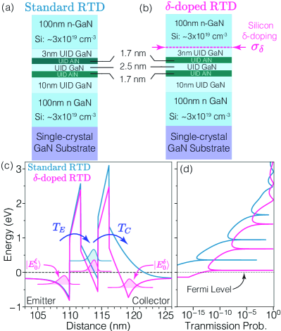
In this Letter, we employ a double-barrier resonant tunneling cavity—shown in Fig. 1(a)—to probe polarization-induced effects on tunneling electrons. In this structure, the broken inversion symmetry of the polarization charges, gives rise not only to a strong electric polarization in the barriers and well, but also induces asymmetric band bending outside the tunneling structure [See the standard resonant tunneling diode (RTD) in Fig. 1(c)]. As a result, electrons traversing the active region undergo highly asymmetric quantum interference effects. The broken-symmetry gives rise to nonreciprocal electronic transport with exponentially asymmetric forward () and reverse () resonant tunneling peaks: Encomendero et al. (2019). Here, we experimentally demonstrate a new GaN/AlN RTD in which symmetric resonant tunneling injection is restored by countering and canceling the polarization asymmetry by doping.
II II. Restoring symmetric quantum interference
Because electronic transmission is exponentially sensitive to the thickness and electric polarization of the tunneling barriers, the standard RTD structure, shown in Fig 1(a) and (c), exhibits highly asymmetric single-barrier transmission coefficients with , where () is the emitter (collector) single-barrier transmission. As a consequence, the electronic wavefunction undergoes partially constructive quantum interference, resulting in a strongly attenuated resonance transmission: Ricco and Azbel (1984); Buttiker (1988); Encomendero et al. (2019). This effect is evident from the transmission probability displayed in Fig 1(d), which also reveals a considerable energy shift due to quantum-confined Stark effect (QCSE) inside the GaN quantum well.
To maximize constructive quantum interference, it is critical to restore the symmetry between the single-barrier transmission coefficients (). One way to achieve this is to increase the doping concentration, thereby reducing the tunneling distance between the well and collector electrode. In this Letter, we aim to completely remove the depletion region on the collector side by inserting a -doped layer Schubert (1994), thereby exponentially enhancing the well-collector coupling strength. This new -doped RTD concept is illustrated schematically in Fig. 1(b). The active region is identical to the standard RTD shown in Fig. 1(a); the only difference between the two stuctures is the incorporation of a sheet of silicon donors with density cm-2. Comparison of the self-consistent energy-band diagrams in Fig. 1(c) reveals that the depletion region is reduced by nm, leading to a smaller tunneling distance and exponentially enhanced wavefunction transmission. A concomitant reduction in the electric field across the AlN barriers is also evident in the -doped RTD. In contrast, the field in the well increases, giving rise to a stronger QCSE. As a result, the ground-state energy approaches the Fermi level, thereby lowering the resonant tunneling voltage. Thanks to the improved symmetry between the tunneling barriers, electrons are expected to undergo enhanced resonant injection with: [See Fig. 1(d)]. Thus, owing to the enhanced tunneling transmission and low-bias resonant injection, symmetric current-voltage (J-V) peaks and negative differential conductance (NDC) are expected under both bias polarities in the -doped heterostructure.
III III. Experiment
Molecular beam epitaxy was used to grow the heterostructures shown in Fig. 1. Both structures were fabricated into diodes following a procedure described elsewhere Encomendero et al. (2018, 2020a, 2021a). The forward-biased circuit of a device under test is shown in the inset of Fig. 2(a). The J-V characteristics in the same figure show that constructive quantum interference and room temperature NDC are attained in both the standard and -doped heterostructures under forward current injection. Owing to the stronger coupling between the resonant states and electrodes, the tunneling current through the -doped RTD is exponentially enhanced under both bias polarities [See Fig. 2(b)]. The cryogenic J-V curves—measured at 4.2 K—reveal that when the -doped structure is biased at V, symmetric resonant tunneling injection and NDC is attained [Fig. 2(c)].
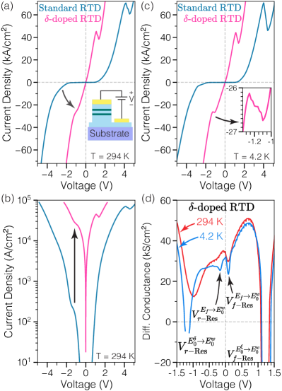
Moreover, in contrast to the highly nonlinear J-V curves in the standard heterostructure, transport in the -doped RTD exhibits an improved linearity and symmetry with respect to the bias polarity. As evident from the inset of Fig. 2(c), the forward and reverse peak current densities are measured at kA/cm2, and kA/cm2, respectively. These resonances correspond to tunneling injection from the emitter and collector subbands [ and in Fig. 1(c)], into the resonant level, . In contrast, resonant injection from the Fermi sea occurs at a lower voltage, close to equilibrium. This can be seen from the differential conductance of the -doped structure, shown in Fig. 2(d). The conductance curves, measured at different temperatures, show clear forward and reverse valleys near zero bias, indicated by the labels and , respectively.
IV IV. -doped RTD model
The physical origin behind the recovery of symmetric resonant injection is explained using a self-consistent analytical model. This theoretical framework elucidates the role of the internal polarization charges in the asymmetric tunneling transport. It also sheds light into the tradeoffs within the design space of noncentrosymmetric polar RTDs.
The collector electric field and the voltage bias for the case of the standard double-barrier heterostructure are related by the expression:
| (1) |
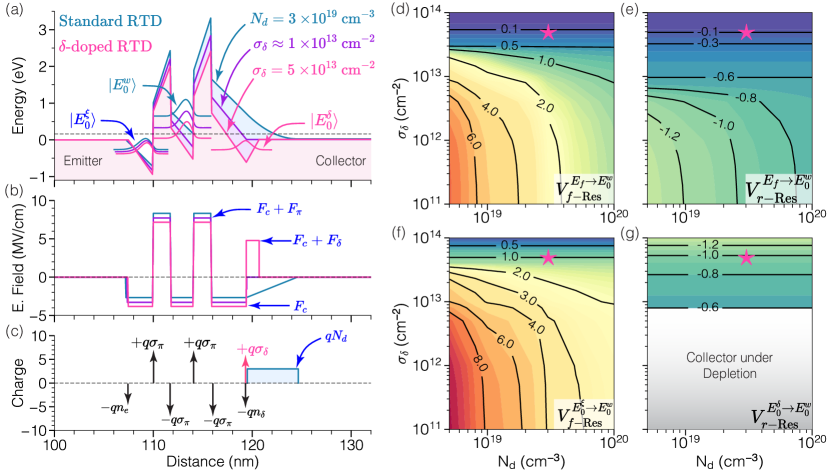
Here, is the contact doping concentration, is the dielectric constant of GaN, and is the internal polarization field. is the total thickness of the double-barrier active region. , , and are the barrier, well, and collector spacer thickness, respectively. The triangular accumulation well on the emitter side, hosts a bound-state with energy , measured from the bottom of the well [See Fig. 3(a)]. Employing a variational approach, we find that , where is the reduced Planck’s constant and is the conduction band-edge effective mass of GaN Schubert (1994). The charge accumulation in the emitter well is captured by its quantum capacitance: .
We note that the first term in Eq. 1 corresponds to the voltage dropped across the depletion region, and scales quadratically with the collector field, . Thus, the space-charge modulation within this region is responsible for the weak voltage-bias tuning of the cavity into resonance; resulting in a larger forward resonant voltage. In contrast to Eq. 1, the functional dependence of in the -doped RTD scales linearly with , and is given by:
| (2) | |||
is the quantum capacitance of the collector -well, whose ground-state eigenenergy reads Schubert (1994). Equations 1 and 2 are of central importance in our analytical model, enabling the calculation of the energy-band diagram, electric field profile, and charge distribution for a general -doped RTD, under equilibrium and non-equilibrium conditions [See Figs. 3(a)-(c)]. Here, we apply this unified theoretical framework to the case of non-centrosymmetric GaN/AlN RTDs.
Figure 3(a) displays the equilibrium energy-band diagrams of different GaN/AlN RTD designs, obtained using our model. The active region of these structures is identical to the devices showcased in Fig. 1(a). Under current injection, the main resonant tunneling peaks originate from the coupling between and the emitter (collector) bound states () Encomendero et al. (2019, 2017, 2021b, 2022); Growden et al. (2020). Detuning from these resonant configurations gives rise to NDC valleys, labeled by and in Fig. 2(d).
Panels (d)-(g) in Fig. 3 display the contour lines of the resonant voltages , , and for the structures shown in Fig. 3(a). The analytical form of our model allows the exploration of the RTD design space as a function of and , over a wide parameter range spanning several orders of magnitude. These results reveal a reasonable agreement between experimental values seen in Fig. 2 and theoretical resonant voltages for all resonances, and under both bias polarities [See Fig. 3(d)-(g)]. As evident from Figs. 3(d) and (f), a monotonic reduction in the forward resonant voltages is obtained as increases over several orders of magnitude. Moreover, for doping levels cm-2, the forward resonant voltages exhibit a strong dependence on the doping concentration . This behavior stems from the inverse dependence between and the collector depletion required to screen the polarization charges within the double-barrier active region in Eq. 1. When the donor sheet density increases beyond cm-2, both and become effectively independent of the 3D-doping level , and are therefore independent of the internal polarization fields. Within this design subspace, only the 2D-doping level controls the forward resonances [See Figs. 3(d) and (f)].
In contrast to the forward injection regime, the reverse-bias resonances ( and ) exhibit dramatically different trends as increases [See Figs. 3(e) and (g)]. Owing to the asymmetric band bending in the standard RTD, electrons injected from the collector side are supplied only by the Fermi sea, resulting in a unique reverse resonant voltage . However as approaches the doping density of cm-2, the collector depletion region is fully suppressed. This can be seen from the energy band diagram labeled as cm-2 in Fig. 3(a). Therefore, RTDs featuring this design attain resonant injection with the whole voltage bias applied across the active region. This distinctive feature enables access to the resonant configurations with the lowest voltage biases. Moreover, the suppression of the depletion region marks a transition in the design space from heterostructures with purely 3D-electron supply to a regime in which both 2D and 3D electrons are injected into the cavity. Beyond this point (i.e. cm-2), increasing results in the formation of a V-shaped -well in the collector electrode. An example of such structure is the -doped RTD shown in Fig. 3(a). In these RTDs, the main reverse-bias resonant peak stems from the coupling between and . Within this design subspace and upon increasing , the energy of the collector subband decreases, resulting in a more negative resonant tunneling voltage in the reverse direction. This behavior is completely captured by our model as can be seen from the larger negative values of as cm-2 [See Fig. 3(g)]. This analysis reveals that collector -doping enables control over the quantum interference properties of polar resonant tunneling cavities, to the extent of attaining resonances independent of the internal polarization fields.
V V. Discussion and conclusions
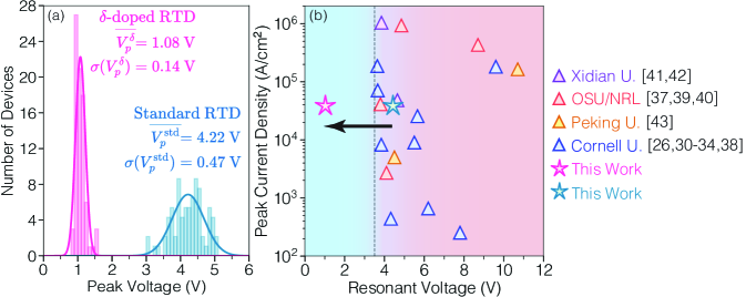
To conclusively demonstrate quantum interference control by -doping, we measure tunneling transport across multiple RTDs with different mesa areas, varying between and m2. Peak tunneling currents from both heterostructures scale linearly with their mesa areas, revealing that electronic transport is mediated by the total area instead of the periphery. Figure 4(a) shows the peak voltage distribution for both RTD designs obtained from a set of 81 devices per sample. Both distributions exhibit a Gaussian behavior, with their dispersion attributed to monolayer fluctuations in the thickness of the AlN barriers and GaN quantum well Song et al. (2016). However, the narrower spread measured in , demonstrates that the -doped design enables not only enhanced tunneling transmission and stronger electrostatic control, but also improved robustness against fluctuations in the resonant tunneling voltage.
Finally, Fig. 4(b) allows us to put these results in context by comparing the resonant tunneling voltages and peak current densities presented here, with previous experimental reports of GaN/AlN RTDs Encomendero et al. (2018, 2020a, 2021a); Growden et al. (2016); Encomendero et al. (2019, 2021b, 2020b, 2017); Growden et al. (2018, 2019, 2020); Encomendero et al. (2022); Zhang et al. (2021a, b); Wang et al. (2018). Owing to the strong internal polarization in the active region, so far these devices have attained resonant tunneling injection at V. The -doped design, introduced in this Letter, enables access to the low-bias resonant tunneling injection regime for the first time.
In conclusion, here we report deterministic control over the electronic quantum interference properties of noncentrosymmetric resonant tunneling heterostructures. A new -doped RTD exhibiting symmetric constructive quantum interference under both bias polarities is unveiled. Due to the stronger coupling between the electrodes and resonant levels, the design not only delivers exponentially enhanced tunneling currents, but also enables stronger electrostatic control and improved robustness against interface roughness. The combined experimental and theoretical approach of this study opens a new avenue for the design and fabrication of robust resonant tunneling effects in noncentrosymmetric polar semiconductors.
VI VI. Acknowledgments
This work was funded by Office of Naval Research (ONR) under the DATE MURI Program (Contract: N00014-11-10721, Program Manager: Dr. P. Maki) and the National Science Foundation (NSF), through the MRSEC program (DMR-1719875). Support from NSF through DMREF (DMR-1534303) and EFRI-NewLAW (EFMA-1741694) programs is also acknowledged. This work was performed in part at the Cornell NanoScale Facility, supported by NSF Grant NNCI-2025233, and Cornell Center for Materials Research Shared Facilities supported through the National Science Foundation (NSF) MRSEC program (DMR-1719875).
References
- Oppenheimer (1928) J. R. Oppenheimer, Physical Review 31, 66–81 (1928).
- Gamow (1928) G. Gamow, Nature 122, 805–806 (1928).
- Zener (1934) C. Zener, Proceedings of the Royal Society A: Mathematical, Physical and Engineering Sciences 145, 523–529 (1934).
- Esaki (1958) L. Esaki, Physical Review 109, 603–604 (1958).
- Tsu and Esaki (1973) R. Tsu and L. Esaki, Appl. Phys. Lett. 22, 562 (1973).
- Chang et al. (1974) L. L. Chang, L. Esaki, and R. Tsu, Appl. Phys. Lett. 24, 593 (1974).
- Tsuchiya et al. (1987) M. Tsuchiya, T. Matsusue, and H. Sakaki, Physical Review Letters 59, 2356–2359 (1987).
- Reuscher et al. (1996) G. Reuscher, M. Keim, F. Fischer, A. Waag, and G. Landwehr, Phys. Rev. B 53, 16414–16419 (1996).
- Slobodskyy et al. (2003) A. Slobodskyy, C. Gould, T. Slobodskyy, C. R. Becker, G. Schmidt, and L. W. Molenkamp, Physical Review Letters 90, 246601 (2003).
- Patanè et al. (2010) A. Patanè, N. Mori, O. Makarovsky, L. Eaves, M. L. Zambrano, J. C. Arce, L. Dickinson, and D. K. Maude, Physical Review Letters 105, 236804 (2010).
- Tao et al. (2019) B. Tao, C. Wan, P. Tang, J. Feng, H. Wei, X. Wang, S. Andrieu, H. Yang, M. Chshiev, X. Devaux, T. Hauet, F. Montaigne, S. Mangin, M. Hehn, D. Lacour, X. Han, and Y. Lu, Nano Letters 19, 3019 (2019).
- Du et al. (2014) R. Du, X. Qiu, A. Li, and D. Wu, Applied Physics Letters 104 (2014), 10.1063/1.4871277.
- Su et al. (2021) J. Su, X. Zheng, Z. Wen, T. Li, S. Xie, K. M. Rabe, X. Liu, and E. Y. Tsymbal, Physical Review B 104, L060101 (2021).
- Sanchez-Santolino et al. (2017) G. Sanchez-Santolino, J. Tornos, D. Hernandez-Martin, J. I. Beltran, C. Munuera, M. Cabero, A. Perez-Muñoz, J. Ricote, F. Mompean, M. Garcia-Hernandez, Z. Sefrioui, C. Leon, S. J. Pennycook, M. C. Muñoz, M. Varela, and J. Santamaria, Nature Nanotechnology 12, 655–662 (2017).
- Blakesley et al. (2005) J. C. Blakesley, P. See, A. J. Shields, B. E. Kardynał, P. Atkinson, I. Farrer, and D. A. Ritchie, Physical Review Letters 94, 067401 (2005).
- Faist et al. (1994) J. Faist, F. Capasso, D. L. Sivco, C. Sirtori, A. L. Hutchinson, and A. Y. Cho, Science 264, 553–556 (1994).
- Yu et al. (2021) X. Yu, Y. Suzuki, M. Van Ta, S. Suzuki, and M. Asada, IEEE Electron Device Letters 42, 982–985 (2021).
- Asada and Suzuki (2016) M. Asada and S. Suzuki, Journal of Infrared, Millimeter, and Terahertz Waves 37, 1185 (2016).
- Xing et al. (2019) H. G. Xing, J. Encomendero, and D. Jena, in Gallium Nitride Materials and Devices XIV, Vol. 10918, International Society for Optics and Photonics (SPIE, 2019) pp. 45 – 50, doi: 10.1117/12.2512638.
- Cho et al. (2020) Y. Cho, J. Encomendero, S.-T. Ho, H. G. Xing, and D. Jena, Applied Physics Letters 117, 143501 (2020).
- Bonnefoi et al. (1985) A. Bonnefoi, T. McGill, and R. Burnham, IEEE Electron Device Letters 6, 636–638 (1985).
- Lind et al. (2004) E. Lind, P. Lindstrom, and L.-E. Wernersson, IEEE Electron Device Letters 25, 678–680 (2004).
- Condori Quispe et al. (2016) H. O. Condori Quispe, J. J. Encomendero-Risco, H. G. Xing, and B. Sensale-Rodriguez, Applied Physics Letters 109, 063111 (2016).
- King-Smith and Vanderbilt (1993) R. D. King-Smith and D. Vanderbilt, Phys. Rev. B 47, 1651–1654 (1993).
- Resta (1992) R. Resta, Ferroelectrics 136, 51–55 (1992).
- Encomendero et al. (2019) J. Encomendero, V. Protasenko, B. Sensale-Rodriguez, P. Fay, F. Rana, D. Jena, and H. G. Xing, Phys. Rev. Applied 11, 034032 (2019).
- Ricco and Azbel (1984) B. Ricco and M. Y. Azbel, Physical Review B 29, 1970–1981 (1984).
- Buttiker (1988) M. Buttiker, IBM Journal of Research and Development 32, 63 (1988).
- Schubert (1994) E. Schubert, in Epitaxial Microstructures, Semiconductors and Semimetals, Vol. 40, edited by A. C. Gossard (Elsevier, 1994) pp. 1–151.
- Encomendero et al. (2018) J. Encomendero, R. Yan, A. Verma, S. M. Islam, V. Protasenko, S. Rouvimov, P. Fay, D. Jena, and H. G. Xing, Applied Physics Letters 112, 103101 (2018).
- Encomendero et al. (2020a) J. Encomendero, D. Jena, and H. G. Xing, “Resonant Tunneling Transport in Polar III-Nitride Heterostructures,” in High-Frequency GaN Electronic Devices (Springer International Publishing, Cham, 2020) pp. 215–247.
- Encomendero et al. (2021a) J. Encomendero, S. Islam, D. Jena, and H. Grace Xing, Journal of Vacuum Science & Technology A 39, 023409 (2021a).
- Encomendero et al. (2017) J. Encomendero, F. A. Faria, S. M. Islam, V. Protasenko, S. Rouvimov, B. Sensale-Rodriguez, P. Fay, D. Jena, and H. G. Xing, Phys. Rev. X 7, 041017 (2017).
- Encomendero et al. (2021b) J. Encomendero, V. Protasenko, D. Jena, and H. G. Xing, Applied Physics Express 14, 122003 (2021b).
- Encomendero et al. (2022) J. Encomendero, V. Protasenko, D. Jena, and G. Xing, in APS March Meeting Abstracts, APS Meeting Abstracts, Vol. 2022 (2022) p. Q68.005.
- Growden et al. (2020) T. A. Growden, D. F. Storm, E. M. Cornuelle, E. R. Brown, W. Zhang, B. P. Downey, J. A. Roussos, N. Cronk, L. B. Ruppalt, J. G. Champlain, P. R. Berger, and D. J. Meyer, Applied Physics Letters 116, 113501 (2020).
- Growden et al. (2016) T. A. Growden, D. F. Storm, W. Zhang, E. R. Brown, D. J. Meyer, P. Fakhimi, and P. R. Berger, Applied Physics Letters 109, 083504 (2016).
- Encomendero et al. (2020b) J. Encomendero, V. Protasenko, F. Rana, D. Jena, and H. G. Xing, Phys. Rev. Applied 13, 034048 (2020b).
- Growden et al. (2018) T. A. Growden, W. Zhang, E. R. Brown, D. F. Storm, K. Hansen, P. Fakhimi, D. J. Meyer, and P. R. Berger, Applied Physics Letters 112, 033508 (2018).
- Growden et al. (2019) T. A. Growden, E. M. Cornuelle, D. F. Storm, W. Zhang, E. R. Brown, L. M. Whitaker, J. W. Daulton, R. Molnar, D. J. Meyer, and P. R. Berger, Applied Physics Letters 114, 203503 (2019).
- Zhang et al. (2021a) H. Zhang, J. Xue, Y. Fu, L. Li, Z. Sun, J. Yao, F. Liu, K. Zhang, X. Ma, J. Zhang, and Y. Hao, Journal of Applied Physics 129, 014502 (2021a).
- Zhang et al. (2021b) H. Zhang, J. Xue, Z. Sun, L. Li, J. Yao, F. Liu, X. Yang, G. Wu, Z. Li, Y. Fu, Z. Liu, J. Zhang, and Y. Hao, Applied Physics Letters 119, 153506 (2021b).
- Wang et al. (2018) D. Wang, J. Su, Z. Chen, T. Wang, L. Yang, B. Sheng, S. Lin, X. Rong, P. Wang, X. Shi, W. Tan, J. Zhang, W. Ge, B. Shen, Y. Liu, and X. Wang, Advanced Electronic Materials 1800651, 1800651 (2018).
- Song et al. (2016) A. Y. Song, R. Bhat, P. Bouzi, C.-E. Zah, and C. F. Gmachl, Physical Review B 94, 165307 (2016).