Thermally-driven phase transitions in freestanding
low-buckled silicene, germanene, and stanene
Abstract
Low-buckled silicene, germanene, and stanene are group graphene allotropes. They form a honeycomb lattice out of two interpenetrating ( and ) triangular sublattices that are vertically separated by a small distance . The atomic numbers of silicon, germanium, and tin are larger to carbon’s (), making them the first experimentally viable two-dimensional topological insulators. Those materials have a twice-energy-degenerate atomistic structure characterized by the buckling direction of the sublattice with respect to the sublattice [whereby the atom either protrudes above () or below () the atoms], and the consequences of that energy degeneracy on their elastic and electronic properties have not been reported thus far. Here, we uncover ferroelastic, bistable behavior on silicene, which turns into an average planar structure at about 600 K. Further, the creation of electron and hole puddles obfuscates the zero-temperature SOC induced band gaps at temperatures as low as 200 K, which may discard silicene as a viable two-dimensional topological insulator for room temperature applications. Germanene, on the other hand, never undergoes a low-buckled to planar 2D transformation, becoming amorphous at around 675 K instead, and preserving its SOC-induced bandgap despite of band broadening. Stanene undergoes a transition onto a crystalline 3D structure at about 300 K, preserving its SOC-induced electronic band gap up to that temperature. Unlike what is observed in silicene and germanene, stanene readily develops a higher-coordinated structure with a high degree of structural order. The structural phenomena is shown to have deep-reaching consequences for the electronic and vibrational properties of those two dimensional topological insulators.
I Introduction
Studies of the topology of the electronic structure originated on two-dimensional Kekulé [1] and hexagonal lattices [2]. Spin-orbit coupling plays a key role on the topology of the electronic band structure [3], and the earliest studies of the effect of spin-orbit coupling (SOC) on a hexagonal lattice (graphene) are due to Huertas-Hernando, Guinea, and Brataas [4], and to Kane and Mele [2]. The latter work emphasized the change of topology of electrons in the valence and conduction bands due to SOC. The SOC strength increases with the atomic number as [5], and it can also be tuned by the curvature induced the two atoms in the unit cell (u.c.) are at a relative height [4]. (The word low-buckled was first introduced in Ref. [6] which published after Ref. [4], and it provides a conventional name for those structures). Graphene’s SOC is small because of carbon’s small , and it is larger on honeycomb lattices containing heavier elements.
Proposals for graphene analogs with strong SOC began appeared early on: low-buckled silicene and germanene’s were first studied in 1994 [7], and low-buckled stanene in 2011 [8]. Nevertheless, germanene and stanene possess what we called a “high-buckled” two-dimensional structural ground state structure with nine-fold coordination (a hexagonal closed-packed bilayer) on their freestanding form [9]. The high-buckled phase for stanene has been suggested to be a two-dimensional superconductor [10]. These two-dimensional materials continue to be explored, with copious experimental work on growth and characterization being reported [6, 11, 12, 13, 14, 15, 16, 17, 18, 19, 20], as well as multiple reviews on the subject [21, 22, 23, 24, 25, 26].
There is still one intrinsic physical quality of freestanding, low-buckled silicene, germanene, and stanene eluding attention though: namely, their propensity to undergo structural phase transformations, which necessarily influence their electronic and vibrational properties. Such study is the topic of this work. In fact, the buckled structure of silicene, germanene, and stanene gives a reason to expect structural transformations: the atomistic energy remains the same upon a mirror reflection with respect to the two-dimensional plane, making these materials structurally degenerate. Structural degeneracies have been found to give rise to structural phase transitions [27, 28, 29, 30, 31, 32, 33, 34], to non-harmonic phonon modes [35], and to softened elastic constants [36, 37].
The manuscript is structured as follows: a description of computational methods is provided in Sec. II. The structural energy of low- and high-buckled silicene, germanene, and stanene is then studied as a function of the two structural parameters (the lattice constant and the buckling height ) at zero-temperature in Sec. III. Such energy information then guides a finite-temperature study of those materials (Section IV) in which the structural, vibrational, and electronic properties are comparatively studied. Conclusions are presented in Sec. V.
II Computational Methods
The study is based on density-functional theory [38] as implemented in the SIESTA code [39], with in-house tuned pseudopotentials [40] in the generalized gradient approximation for the exchange-correlation functional due to Perdew, Burke, and Ernzerhof [41].
II.1 Zero-temperature calculations
Zero-temperature calculations were first carried out to understand the elastic energy landscape and vibrational properties of low-buckled structures within the harmonic approximation. Zero-temperature phonon calculations within the harmonic approximation utilized a rectangular supercell and atomic displacements of either 1.0 Bohr (silicene and germanene) or 0.9 Bohr (stanene).
II.2 Finite-temperature calculations
Ab initio molecular dynamics (MD) calculations within the isothermal-isobaric (NPT) ensemble were carried out at standard ambient pressure. Temperature was controlled by a Nosé thermostat, while a target pressure was set using the Parinello-Raman method [42]. We opted away from a supercell having a diamond shape for one with a configuration close to a square, and set up a 712 supercell using a non-primitive rectangular cell containing four atoms and in-plane lattice vectors and [with the lattice constant of the primitive unit cell (u.c.) at zero temperature], which correspond to the armchair and zigzag directions, respectively. The 712 supercells we built have an almost one-to-one horizontal/vertical aspect ratio, spanning an area , and contain 336 atoms. We initialized atomic positions in the low-buckled two-dimensional silicene, germanene, or stanene structure shown on Fig. 1(b)(i). The out-of-plane lattice vector had a length of 15 Å.
MD calculations were carried out at temperatures ranging from 200 K to 900 K for silicene, 100 K to 675 K for germanene, and 100 K to 400 K for stanene. A MD time step length of 1.5 fs was used, unless indicated otherwise. The instantaneous temperature, the energy per primitive u. c., as well as and were tracked. is a signed height obtained with the procedure given in Appendix A. Pair-correlation functions were computed as well, to hint of structural transitions onto three-dimensional or disordered phases. Those were obtained for all frames after 20 ps, by counting the number of neighboring atoms located at a distance at a given value in between 0 Å to , with a resolution. The count was normalized by .
We also employed a non-perturbative method to obtain the natural vibrational frequencies of these materials at finite temperature, relying on the power spectrum of the velocity autocorrelation function within MD trajectories. The power spectrum is obtained at a discrete set of points by (i) Fourier transforming atomic velocities, (ii) carrying out a time autocorrelation, and (iii) Fourier transforming the resulting function into frequency space [43]. The process has been employed to determine finite-temperature behavior of ferroic 2D materials, in which softening of specific vibrational modes has been observed [30, 32].
The electronic structure was calculated on one hundred primitive u.c.s. Each u.c. contains the average atomic positions of a supercell at a fixed time during the structural time-evolution. The use of multiple unit cells permits capturing structural fluctuations as time evolves, and each bandstructure at a given time is independently plotted to make such fluctuations observable. Those structures were obtained at times equally spaced within 300 fs after thermal equilibration.
III Atomistic structure and energy degeneracies
Figure 1(a) shows side and top views of a planar honeycomb structure. A primitive unit cell has been indicated by a diamond on the top view plot, with atoms on the and sublattices indicated as well. The buckling height is an order parameter, a signed measure of the relative displacement among and sublattices along the direction, and it has a zero magnitude for planar structures: Å. Fig. 1(b) depicts two degenerate three-fold coordinated, low-buckled structures, which are determined by two structural parameters: , and , which is greater than zero on Fig. 1(b)(i), and smaller than zero on Fig. 1(b)(ii). We define to be positive when the atoms sit above the atoms on the zero-temperature (initial MD frame) structure. A non-primitive, rectangular unit cell is shown in dashed lines on the top view as well. Fig. 1(c) shows two degenerate high-buckled, nine-fold coordinated two-dimensional structures [40].
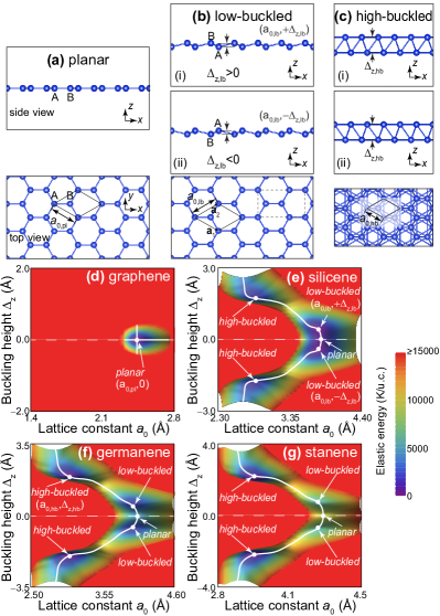
Figures 1(d) through 1(g) display elastic energy landscapes for graphene, silicene, germanene, and stanene, respectively. Energy landscapes were obtained by stretching the two in-plane primitive lattice vectors by the same amount–this is, by increasing the lattice constant only, without changing the angle among primitive lattice vectors and [see Fig. 1(b)]–while maintaining an identical distance and angular separation among the atoms belonging to opposite sublattices. Under those constraints, the lattice constant is shown as the horizontal axis, while is represented by the vertical axis, and the false color serves to indicate the relative depth of global and/or local minima for each of these four two-dimensional materials. The landscapes on Figs. 1(d) through 1(g) are similar to those published for other 2D materials with structural degeneracies before [27, 29, 30, 34].
Energy densities on Figs. 1(d-g) are reported in units of K/u.c., because a comparison of these values with critical temperatures obtained via molecular dynamics (obtained with the same ab initio numerical tool) gives a relation among the barriers obtained from the landscapes and of the order (see Refs. [27, 29, 44] and [33] for group-IV monochalcogenide monolayers; Refs. [45, 30, 36] for SnO monolayers, and Ref. [34] for ferroelectric transition metal dichalcogenide bilayers). Areas on the landscape for which the energy exceeds 15,000 K/u.c. are just shown in red. (This upper limit makes sense as the temperature at the sun’s surface is close to 6,000 K, and at that temperature materials would have long melted down). As seen on Figs. 1(e-g), the local minima can be traveled about within a “trench” on the energy landscape, and all the available local minima for buckled, hexagonal configurations are included in those plots. A one-dimensional path of steepest descent–similar to those drawn in Refs. [29] and [30]–is shown in white as well.
To motivate the usefulness of the elastic energy landscape, and as seen on Fig. 1(d), graphene has a single (non-degenerate) structural ground state with a planar structure; a result that is expected. Silicene, on the other hand, displays two degenerate global minima upon a change of sign on in the low-buckled configuration [Fig. 1(e)]. These two distinguishable structures are related by a reflection with respect to the plane, and may be switchable (making silicene a new ferroelastic two-dimensional material) by a deformation whereby the lattice constant increases slightly and the order parameter becomes zero on average.
| Material | (Å) | (Å) | (Å) | (K/u.c.) |
|---|---|---|---|---|
| graphene | — | 0.000 | 2.475 | — |
| silicene | 3.870 | 0.482 | 3.902 | 621 |
| germanene | 4.081 | 0.710 | 4.154 | 3687 |
| stanene | 4.676 | 0.896 | 4.831 | 4541 |
| Material | (Å) | (Å) | (K/u.c.) |
|---|---|---|---|
| silicene | 2.688 | 2.143 | 1784 |
| germanene | 3.022 | 2.246 | 1621 |
| stanene | 3.436 | 2.613 | 5448 |
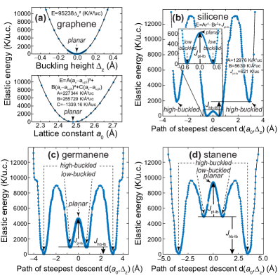
To start arguing for ferroelastic behavior on silicene–and for a possible two-dimensional phase transformation on this two-dimensional material–Fig. 2 shows the elastic energy along the one-dimensional steepest descent paths depicted on Fig. 1(d) through Fig. 1(g). While graphene [Fig. 2(a)] has a single, non-degenerate energy minima on this landscape, silicene, germanene, and stanene display four local minima corresponding to low-buckled or high-buckled configurations.
As seen on Fig. 2(b), the energy region shown for low buckled silicene around Å displays an (anharmonic) double-well potential, which was fitted to:
| (1) |
The existence of two minima at Å is a prelude of the bistable behavior of this 2D material [29, 30], especially due to the low magnitude of the energy barrier =621 K/u.c. (see Table 1), which corresponds to . Now, although germanene and stanene also have local minima at their low-buckled conformations, the barrier among them listed in Table 1 is significantly higher (hindering the appearance of an average planar configuration), and high-buckled structures lie lower in energy. The differences in each subplot on Fig. 2 underscore what should be different, distinct possible finite-temperature behaviors for each of those two-dimensional materials.
Table 1 lists the optimal structural parameters at ; i.e., at the (global or local) minima for low-buckled structures (with positive and negative signs on indicating the inherent two-fold structural degeneracy), the lattice constant for the optimal (lowest energy) planar structure, and the energy (in units of Kelvin per primitive u.c.) needed to reach the planar structure from any of the degenerate low-buckled ones; see Fig. 1. Prior experience tells us that a critical temperature for a two-dimensional phase transformation onto another structure will be of the same order of magnitude than the barrier , when is smaller than the melting point. is depicted in Fig. 2. According to Table 1, one may observe a transformation onto planar freestanding silicene at temperatures above 621 K.
Consistent with previous work [9], the high-buckled phases–defined by the coordinates on Fig. 1–become preferable two-dimensional structure as the atomic mass of group-IV elements increases–see Figs. 2(c) and 2(d). This statement is made quantitative by reporting the energy difference on Table 2: As seen on Fig. 2, negative values of indicate a lower energy of the high-buckled 2D phase for both germanene and stanene. The consequence of the low-buckled phase turning metastable is that–starting on a low-buckled structure–germanene and stanene may melt, become amorphous, or turn into their high-buckled phase, rather than turning planar. Results of MD calculations, to be described next, shed light into the finite-temperature behavior of freestanding, low-buckled group-IV materials.
IV Structural behavior of freestanding silicene, germanene, and stanene at finite temperature
We now contrast the information provided on Fig. 1, Fig. 2, Table 1, and Table 2, with the finite-temperature behavior of low-buckled silicene, germanene, and stanene. This comparative study contains (i) instantaneous temperature, structural energy, supercell-averaged lattice constants for the primitive unit cell , and supercell-averaged buckling height as a function of time at selected target temperatures; (ii) structural snapshots and pair-correlation functions; (iii) the evolution of and of as a function of temperature, to observe or discard a low-buckled-to-planar two-dimensional transition; and (iv) electronic structures. These four sets of information will be provided gradually for silicene (Sec. IV.1), germanene (Sec. IV.2), and stanene (Sec. IV.3) in what follows.
IV.1 Silicene’s finite-temperature behavior
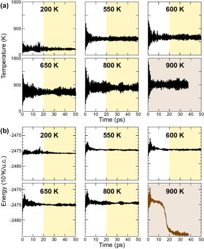
Fig. 3(a) displays the instantaneous temperature over a period of up to 50 ps for silicene supercells set at 200 K, 550 K, 600 K, 650 K, and 800 K, respectively. An additional plot at a target temperature of 900 K ends shortly before 40 ps for reasons that will be made clear in a moment. The takeaway point from Fig. 3(a) is that there are dramatic temperature fluctuations for the first 10 ps, and thermal equilibration sets in for longer times. Fig. 3(b) shows the time evolution of the instantaneous total energy per primitive u.c. at 200 K, 550 K, 600 K, 650 K, 800 K, and 900 K: the total energy steadily increases with temperature for target temperatures up to 800 K. The marked decrease of the instantaneous total energy at 900 K on Fig. 3(b) is a sign of a sudden atomistic reconfiguration onto a more energetically favorable structure. Since atomistic forces on ab initio MD necessitate the convergence of the electronic density, we decreased the time step from 1.5 fs down to 0.5 fs at this higher temperature (since a smaller time step implies a smaller displacement, and an easier to converge electron density at each consecutive MD step), and collected the dynamics up to a shorter time as a result. Nevertheless, the relative flatness of the instantaneous energy above 30 ps on Fig. 3(b) at 900 K indicates that a further sudden drop of the total energy may not occur within the time window studied.
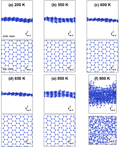
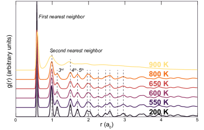
To link the total energy to atomistic configurations, Fig. 4 shows side and top view snapshots of the silicene supercell taken at the last simulated frame, at temperatures consistent with those shown on Fig. 3. The hexagonal lattice is visible at most temperatures, and the sudden drop of the total energy at 900 K on Fig. 3(b) is linked with a transition onto an amorphous phase [Fig. 4(f)], further confirmed by the pair-correlation functions depicted on Fig. 5, which were vertically offset to better convey that the atomistic coordination remains almost unaltered for temperatures up to 800 K.
We argue that a two-dimensional phase transformation onto an average planar structure is taking place at around 600 K. Unveiling it requires paying close attention to the order parameter amounting to the relative height among atoms belonging to opposite sublattices including sign. Details follow.
IV.1.1 Relative height of the two atoms in the unit cell as an order parameter
As a starting configuration, all supercells have all atoms above atoms at the onset of MD calculations [Fig. 1(b)(i)]. This means that every u.c. has a positive value of on Fig. 2(b). This assertion is verified on Figs. 1(e-g), which show a value of the order parameter . Correspondingly, negative values of on Fig. 2 imply that all atoms on a crystal sit “below” nearest neighboring atoms. Identification of “above” and “below” is straightforward on an ideal crystal at zero temperature [in this particular situation, gives away if the atom is above (), below (), or if the structure is planar (), where () is a position vector for any () atom, and ], and it requires defining the projection of the position vector of atoms onto local signed normals set by the planes defined by the three closest atoms at finite temperature. (Initial structures for which a section contains atoms above atoms, while another section contains atoms above atoms, will have domain walls in which a pair of neighboring and atoms reside at the same height. Structures containing those domain walls were not considered here.)
While the supercells for MD calculations are originally set with at every primitive u.c. (no domain behavior was considered), identification of unit cells for which [ on Fig. 3(b))] at finite temperature imply that atoms (originally above atoms) would have sufficient elastic energy to jump the double potential well on some u.c.s of the supercell and turn below atoms. This means that atoms on those u.c.s would be exploring the region on Fig. 2, setting the material at the onset of a two-dimensional structural transformation [29, 30]. Details follow.
IV.1.2 Transformation onto a planar two-dimensional silicene on average at a critical temperature
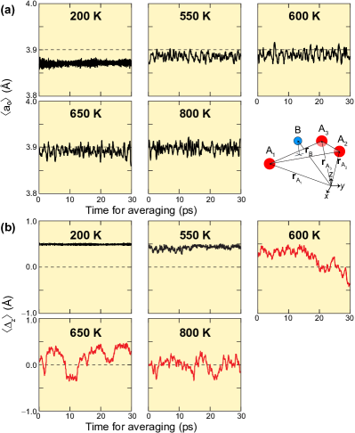
A hexagonal lattice is created by two interconnected triangular lattices, and an atom belonging to the sublattice with coordinates is always neighboring three atoms on the sublattice (, , and ) with coordinates , , and . As seen on the lower-right inset on Fig. 6(a), we choose the labels on the sublattice atoms to run counter-clockwise. Then, local lattice vectors and are defined as:
| (2) |
Local vectors and fluctuate at finite temperature. Panels on Fig. 6(a) display the lattice constant at finite temperature, which is obtained at each time step as the average of all possible local magnitudes of and within the supercell. Fluctuations of are due to the fact that the containing walls are not fixed on the NPT ensemble, allowing for the low-buckled silicene supercell to slightly expand and compress as time goes on. The horizontal dashed line on Fig. 6(a) indicates the zero-temperature value of for planar silicene listed on Table 1, and one observes that raises onto as temperature increases.
Determining requires specifying the direction of the local plane defined by the three atoms , , and , and one gets one value of per primitive u.c. We define the local plane’s normal as:
| (3) |
(Note that is anti-parallel to .) The (signed) local buckling height is generalized for tilted honeycomb lattices at finite temperature as:
| (4) |
See Appendix A for details. Figure 6(b) displays the average height over the supercell at a given temperature and time, revealing a situation in which suddenly fluctuates among positive and negative values for temperatures of 600 K or larger.
Figure 7(a) shows and its standard deviation, taken for the 20,000 frames captured within the last 30 ps (this is, after thermal equilibration; this time interval shown in yellow on Figs. 3 and 6). The dashed horizontal line on Fig. 7(a) once again indicates that the lattice constant of silicene steadily approaches the magnitude of the zero-temperature planar structure, , as temperature increases. Å at ambient conditions.
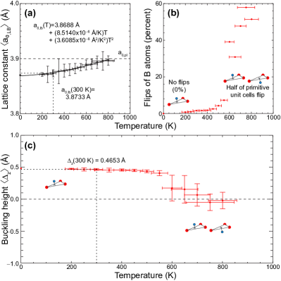
As indicated earlier on, we originally set the silicene structure at the configuration indicated by a “low-buckled” label for [Fig. 1(b)(i); point on Fig. 1(e); and Å on Fig. 3(b)]. Furthermore, Table 1 indicates that the planar structure can be created by adding and energy of 621 K per primitive unit cell. If that energy could be facilitated thermally, one would expect to reach a dynamical situation in which both low-buckled structural configurations [one in which as in Fig. 1(b)(i); another in which as in Fig. 1(b)(ii)] could be accessible with equal (50%) probability. As seen on Fig. 7(b), such scenario takes place indeed. It reminisces of the 2D transformations discussed in Refs. [27, 28, 31, 29] and [30] for other 2D materials in which a double-well potential with a small barrier is crossed at finite temperature, unleashing 2D transformations of the order-by-disorder type. Indeed, close observation to fluctuations of lattice parameters in Refs. [28] and [30] indicates that square unit cells are, in fact, time averages of highly-fluctuating rectangular unit cells. Here, a planar structure is the average result of floppy vibrational modes enabled by a shallow degenerate wells on a Landau-type, similar elastic potential [inset on Fig. 2(b)].
Fig. 7(c) shows the collapse of the order parameter , further confirming the similarity of the phenomena observed in silicene and other phase-changing 2D materials [27, 28, 29, 30, 34] (see Table 3 for a comparison). The collapse of past 600 K further confirms the use of the barrier among planar and low-buckled silicene to provide valuable intuition into the magnitude of the critical temperature. We are unaware of previous reports indicating such a two-dimensional structural transformation on silicene. At this point, we remind the reader that silicene is turning amorphous at 900 K (Fig. 4(f)), and that the barriers for both germanene and stanene exceed 3,500 K/u.c. (Table 1): one should not expect a transition like the one we just documented for silicene on those other two-dimensional materials.
| 2D Material | Degeneracy | Order par. | Coord. change? |
|---|---|---|---|
| SnO[45, 30] | Two-fold | No | |
| SnSe[33] | Two-fold | 3-fold to 5-fold | |
| TMDC | Infinite | Interlayer | No |
| bilayers[46, 34] | displacement | ||
| silicene | Two-fold | No |
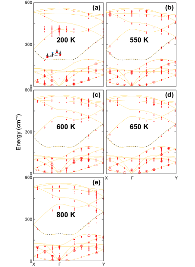

The existence of degenerate minima and a thermally reachable energy barrier necessarily guarantees anharmonic vibrational properties, and a strong electron-phonon coupling [32]. Fig. 8 shows both the vibrational spectra of low-buckled silicene as obtained within the harmonic approximation (yellow curves), and that obtained from the non-perturbative power spectrum of the velocity autocorrelation approach [43] shown in (red) circles. The circles indicate the relative peak intensity, and the coalescence of multiple circles around a given zero-temperature phonon line is indicative of the lifetime of the vibrations obtained from MD. The choice of a rectangular cell on MD simulations was deliberate, as we wanted to simulate a near-square structure with equal dimensions to permit vibrations that could be homogeneous along the and directions.
The softening of specific bands can be seen in multiple suplots of 8. See, for instance, the dotted band corresponding to the out-of-plane optical mode, which softens in all plots (taking the average separation between the visible finite-temperature points and the continuous, zero-temperature lines on Fig. 8, it becomes smaller by 3.35 cm-1 at 200 K, 4.17 cm-1 at 550 K, 6.87 cm-1 at 600 K, 5.40 cm-1 at 650 K, and 9.26 cm-1 at 800 K).
IV.1.3 Consequences for the SOC-induced bandgap
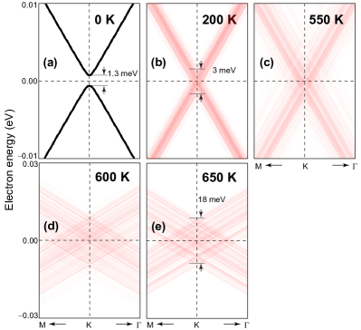
The broadening of finite-temperature vibrational eigenmodes hinted at on Fig. 8 should also broaden the electronic dispersion. To begin with, oscillations create strain and curvature, giving rise to electron-hole puddles arising from inhomogeneities of the local deformation potential on 2D materials [47, 48, 49, 50, 51]. Those fluctuations of the deformation potential may be larger than silicene’s zero-temperature 1.3 meV band gap, and it is a point we have not seen raised in the literature. In addition and according to Huertas-Hernando, Guinea, and Braatas, the intrinsic spin-orbit coupling can be greatly enhanced by buckling [4], and diminished in planar configurations.
Following an ergodic assumption–i.e., that spatial averages give equivalent results to time averages–and using the method delineated in Appendix B, we present what perhaps is the most surprising result from the present work: that atomistic vibrations obfuscate the 1.3 meV SOC-induced band gap of low-buckled silicene; this average closing of the SOC-induced bandgap occurs at a temperature as low as 200 K [Fig. 9(b)]. In addition, SOC band gaps depend on curvature [4], and close on the planar configuration. This effect is clearly seen by comparing subplots 9(a) with 9(d) and 9(e). The net fluctuations of the deformation potential are listed in Table 4 at Appendix B. That the minuscule band gap of silicene will be obscured by fluctuations of the deformation potential is an unquestionable result.
It is time to discuss how low-buckled germanene and low-buckled stanene behave at finite temperature in comparison. At this point, most methods have been introduced, which will give us the opportunity to mostly focus on different behaviors with respect to those seen in silicene.
IV.2 Germanene’s finite-temperature behavior
It is time to refer, once again, to Tables 1 and 2, and to Figs. 1(f) and 2(c). To begin with, the barrier to turn into a planar structure is much higher in germanene (3687 K/u.c.) than it is for silicene (621 K/u.c.): this should imply that one is not to observe a transition from a low-buckled onto a planar germanene phase. Furthermore, while the low-buckled phase of silicene was more stable than its high-buckled one [9], the negative sign of for germanene in Table 2 says that a high-buckled phase should be more stable than the low-buckled structure set at the start of the MD evolution.
Figure 10(a) shows the instantaneous temperature of germanene along the molecular dynamics simulation. As seen on Fig. 10(b), the finite-temperature behavior of low-buckled germanene indicates a transition onto a lower-energy phase at 675 K, which is a lower temperature than that in which we observed the creation of amorphous silicon (900 K; see Fig. 4). Furthermore, for temperatures up to 650 K, germanene never reaches a transition into a planar structure given that =3687 K/u.c. [see the distance to the horizontal dashed line on Fig. 10(c), and that never ever reduces its zero-magnitude value on Fig. 10(d)]. Verification of a transition of germanene onto an amorphous phase at 675 K is provided on Fig. 11(e), as well as on Fig. 12. The fact that a transition onto an amorphous phase [see the sudden broadening of in the 675 K trace on Fig. 12] takes place is related to the fact that the high-buckled phase is a ground state here, and that low-buckled germanene is a local (metastable) two-dimensional configuration; see Fig. 2(c).


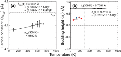
Figure 13 demonstrates that thermal expansion alone is not sufficient for germanene to undergo a transition onto a planar structure: the expansion seen on Fig. 13(a) is not sufficient to reach the magnitude displayed as a horizontal line up to the temperature at which it melts. Nevertheless, on Fig. 13(b) remains almost unchanged up to the melting point. The lack of flips on germanene is explained by the tall elastic energy barrier observed on Fig. 2(c) and reported in Table 1. That it melts at a lower temperature than silicene may be underpinned by the fact that the low-buckled phase is a metastable one. Ambient values of and of (4.0892 Å, and 0.7091 Å, respectively) can be found in Fig. 13 as well.
Figure 14 shows the vibrational properties of low-buckled germanene. Here, the softening of vibrational bands can be seen in a similar way than in silicene. For example, the dotted band, corresponding to the optical out-of-plane mode softens as a function of temperature as follows: by -1.36 cm-1 at 100 K, -6.19 cm-1 at 500, -10.88 cm-1 at 600, and by -10.72 cm-1 at 650 K.


As for germanene’s electronic properties, Fig. 15 indicates that the SOC-induced 20 meV band gap persists up to the melting point up to 650 K, despite of the observed phonon-induced broadening, which is as large as 8 meV at 650 K and it is due to fluctuations of the deformation potential only. That silicene has a larger broadening at similar temperatures is a combined result of the deformation potential and the sudden changes in curvature; see Huertas-Hernando et al. [4].
This manuscript ends with a comparative discussion of low-buckled stanene at finite temperature.
IV.3 Stanene’s finite-temperature behavior

We refer to Tables 1 and 2 one more time, and to Figs. 1(g) and 2(d), to continue making the point that they contain crucial information that can be used to understand the finite-temperature behavior of low-buckled, freestanding, group-IV monoatomic two-dimensional materials.
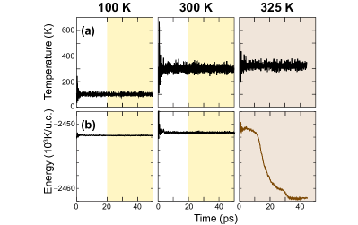
The barrier to transition from a low-buckled onto a planar stanene configuration is a prohibitive 4541 K/u.c. now. Furthermore, the high-buckled structure is now at a much lower, 5448 K/u.c. below the low-buckled phase. This way, and as seen on Fig. 16, low-buckled stanene transitions onto another phase at just 325 K, without undergoing an intermediate planar phase (for which ) in the interim. The structural plots at 325 K on Figure 17 confirm this observation, although a larger degree of order is observed when contrasted to silicene at 900 K [4(f)], or to germanene at 675 K [Fig. 11(e)].
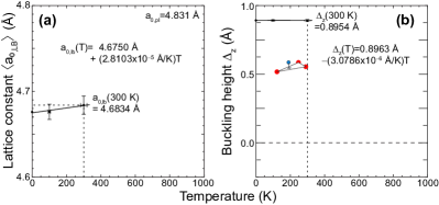

Figure 18 contains average values for stanene’s lattice constant and the buckling height, when started at the low-buckled configuration, and before it turns into the ordered, thicker phase observed on Fig. 17(c). One observes the thermal expansion of and an almost constant value of , which remains stiff as in the case of germanene [Fig. 13] due to the even taller elastic energy barrier K/u.c. [see Table 1], and unlike silicene [Fig. 7(c)] which was shown to undergo a transition whereby 50% of the atoms are above atoms and 50% lie below on average. The lattice constant and buckling height are equal to 4.6834 Å and 0.8954 Å at ambient conditions.
The temperature-dependent pair correlation functions shown in Fig. 19 differ from those shown on Figs. 5 and 12, in that peaks develop at different distances, as opposed to the gradual blurring that was observed for silicene and germanene. The displacements of the peaks that are observed in Fig. 19 support the fact that a new, thicker and (hexagonal-closed-packed) bulk-like phase is being generated on tin at 325 K. This fact is further confirmed by showing a pair correlation function at a higher temperature of 400 K.
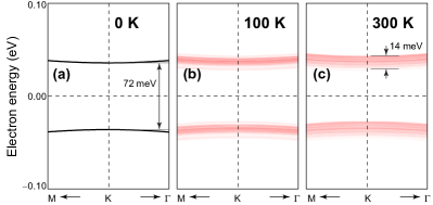
The last point of discussion concerns the vibrational and electronic properties of low-buckled stanene prior to its structural transition onto a thicker structure. Figure 20 shows that the vibrational modes are consistent with those of the low-buckled structure up to room temperature, and the mode highlighted by dotted lines softens by 0.56 cm-1 at 300 K, and by 3.01 cm-1 at 300 K. Figure 21 shows that the 72 meV SOC-induced bandgap remains robust despite of the electron-phonon coupling because of the lack of vertical flips [see Fig. 18(b)].
This way, we have provided a crucial assessment of 2D topological insulators at finite temperature, and provided guidance as to possible structural transformations that may affect intended topological properties of those materials on their freestanding form. The observations made using MD on this work support and complement those made earlier on [9].
V Conclusion
Exhaustive molecular dynamics simulations and zero-temperature calculations were employed to understand the finite-temperature behavior of silicene, germanene, and stanene, initially set into their low-buckled atomistic configuration. The structural degeneracy (positive and negative buckling) suggested a possibility of ferroelastic behavior on these materials, anharmonic vibrational properties, and phase transitions.
Ferroelastic behavior, and a transition onto an average planar 2D structure was indeed observed in freestanding low-buckled silicene above 600 K. Numerical evidence shows that it melts at 900 K. We also found that the 1.3 meV SOC-induced bandgap of silicene is smaller in magnitude than fluctuations of the local deformation potential, which will hinder observation of said bandgap at temperatures as small as 200 K.
The high-buckled two-dimensional structure is preferable for germanene and stanene. Germanene reaches its melting phase transformation at 675 K, and it does not transition onto a planar phase at intermediate temperatures. The SOC-induced bandgap is robust against thermal oscillations.
Stanene reconfigures itself above room temperature (325 K) into a bulk HCP crystal, as is expected of heavier metallic materials. We did not observe ferroelastic behavior for germanene nor stanene.

Those results could be useful to link these material’s expected atomistic and electronic structure at finite temperature (especially considering operation temperatures on actual devices), and gives information about expected phase transitions onto planar 2D structures (silicene), disordered ones (silicene and germanene), or bulk (stanene) phases.
VI Acknowledgments
We thank Dr. Pradeep Kumar for insightful conversations, and Shiva P. Poudel for technical assistance. Work funded by the U.S. Department of Energy (Award DE-SC0022120).
Appendix A Determination of the local value of
Taking the normal to the plane defined by atoms , , and as given in Eqn. (3), the equation of the plane spanned by these three points is given by:
| (5) |
In Eqn. (5), is a coordinate within the plane. Indeed, Eqn. (5) can be used to solve for, say, as a function of and ; and then become the two independent variables defining the plane.
We next need to determine whether point lies “below” or “above” the plane defined by , , and . Quotation marks are added because, as seen on the side views of Figs. 4, 11, and 17, the planes defined by any three neighboring atoms on the sublattice tilt with respect to the plane one had at zero temperature, requiring additional clarification on the meaning of an atom being “up” or “down” a plane. We will use the normal vector to set a formal definition of an atom being up or down a plane next.
To do so, we need to find a specific point within the plane, which we will call , such that the distance between point and takes its minimum value. This condition occurs when the vector is parallel or antiparallel to .
Now, a parametrization of a straight line containing the vector is given by , with a real number. This line does not necessarily pass through point though. Nevertheless, the following straight line:
| (6) |
will pass through when and, being parallel to the plane’s normal, it will pierce through the plane spanning the smallest distance among the point and the plane. Let’s parameterize that special value for as . Then, Eqn. (5) turns more specific (because the intersection of a plane and a straight line is a point), and it helps us determine explicitly. Indeed, substituting for the equation of the straight line, Eqn. (6) for the value of for which the line pierces the plane, we get:
| (7) |
which can be simplified into
| (8) |
This way, plugging the value of found in Eqn. (8) into Eqn. 6, the closest point to within the plane (which we will call ) ends up being given by:
| (9) |
so the shortest vector between point and (i.e., ) ends up being
| (10) |
is the projection of into the local normal :
| (11) |
where was employed. Eqn. (11) formalizes the concept of “up” or “down” for every atom within the supercell, at any temperature, and at any time, as long as the supercell does not turn amorphous.
Appendix B Band broadening arising from deformation potential
| Material | Temperature (K) | (eV) | (eV) |
|---|---|---|---|
| silicene | 200 | 0.0001 | 0.0009 |
| silicene | 550 | 0.0002 | 0.0026 |
| silicene | 600 | 0.0000 | 0.0060 |
| silicene | 650 | 0.0001 | 0.0052 |
| germanene | 100 | 0.0000 | 0.0012 |
| germanene | 500 | 0.0000 | 0.0022 |
| germanene | 600 | 0.0000 | 0.0025 |
| germanene | 650 | 0.0000 | 0.0020 |
| stanene | 100 | 0.0000 | 0.0010 |
| stanene | 300 | 0.0000 | 0.0013 |
We follow the process introduced in Ref. [49] to estimate band broadening due to finite-temperature atomistic motion. Here, we use one hundred snapshots, equally separated, and create a primitive unit cell using the average lattice constant and buckling height per snapshot. The distance among three neighboring atoms on each of these average primitive unit cells is called .
We also calculate the electron hopping integral at zero temperature, by fitting the linear dispersion of these materials away from the gap (they all obey a Dirac Equation for fermions with mass). In that linear region, the electron’s velocity (known as Fermi velocity ) is given by , and the hopping integral is
| (12) |
with the zero-temperature lattice constant from Table 1. Furthermore, .
With this procedure, we found eV for low-buckled silicene, t=0.954 eV for low-buckled germanene, and t=0.744 eV for low-buckled stanene, and the deformation potential is estimated as a linear deviation related to the average change in interatomic distances on the unit cell:
| (13) |
which is adapted from Ref. [49]. A reduction of the size of the unit cell makes and increases the electron cloud density, which results on electron repulsion and a local upshift of the chemical potential [Eqn. (13)], for an electron-deficient region. Alternately, an increase of the size of the unit cell makes and decreases the local electron density, which results on a downshift of , and an electron-rich region. See Refs. [48, 49, 50] for more details.
On a real material, there are electron-rich and electron-rich regions [see, e.g., Refs. [47, 48, 49, 50, 51]], which make the local conduction and valence band fluctuate with respect to the midgap. Assuming ergodic behavior, we calculate the electronic structure on a given average primitive unit cell, and extract the band lifetime and the effects of electron-phonon coupling at finite temperature as listed in Table 4.
References
- Haldane [1988] F. D. M. Haldane, Model for a quantum hall effect without landau levels: Condensed-matter realization of the ”parity anomaly”, Phys. Rev. Lett. 61, 2015 (1988).
- Kane and Mele [2005] C. L. Kane and E. J. Mele, Quantum spin hall effect in graphene, Phys. Rev. Lett. 95, 226801 (2005).
- Shen [2013] S. Shen, Topological Insulators: Dirac Equation in Condensed Matters, Springer Series in Solid-State Sciences (Springer, Heidelberg, Germany, 2013).
- Huertas-Hernando et al. [2006] D. Huertas-Hernando, F. Guinea, and A. Brataas, Spin-orbit coupling in curved graphene, fullerenes, nanotubes, and nanotube caps, Phys. Rev. B 74, 155426 (2006).
- Tserkovnyak et al. [2005] Y. Tserkovnyak, A. Brataas, G. E. W. Bauer, and B. I. Halperin, Nonlocal magnetization dynamics in ferromagnetic heterostructures, Rev. Mod. Phys. 77, 1375 (2005).
- Cahangirov et al. [2009] S. Cahangirov, M. Topsakal, E. Aktürk, H. Şahin, and S. Ciraci, Two- and one-dimensional honeycomb structures of silicon and germanium, Phys. Rev. Lett. 102, 236804 (2009).
- Takeda and Shiraishi [1994] K. Takeda and K. Shiraishi, Theoretical possibility of stage corrugation in si and ge analogs of graphite, Phys. Rev. B 50, 14916 (1994).
- Garcia et al. [2011] J. C. Garcia, D. B. de Lima, L. V. C. Assali, and J. a. F. Justo, Group iv graphene- and graphane-like nanosheets, J. Phys. Chem. C 115, 13242 (2011).
- Rivero et al. [2014] P. Rivero, J.-A. Yan, V. M. García-Suárez, J. Ferrer, and S. Barraza-Lopez, Stability and properties of high-buckled two-dimensional tin and lead, Phys. Rev. B 90, 241408 (2014).
- Liu et al. [2022] C. Liu, P.-F. Liu, X.-H. Tu, L. Shang, P. Zhang, W. Ren, and B.-T. Wang, First-principles prediction of superconductivity in high-buckled two-dimensional tin, ACS Appl. Elec. Mater. 4, 2062 (2022).
- Dávila et al. [2014] M. E. Dávila, L. Xian, S. Cahangirov, A. Rubio, and G. Le Lay, Germanene: a novel two-dimensional germanium allotrope akin to graphene and silicene, N. J. Phys. 16, 095002 (2014).
- Roome and Carey [2014] N. J. Roome and J. D. Carey, Beyond graphene: Stable elemental monolayers of silicene and germanene, ACS Appl. Mat. Int. 6, 7743 (2014).
- Ma et al. [2012] Y. Ma, Y. Dai, M. Guo, C. Niu, and B. Huang, Intriguing behavior of halogenated two-dimensional tin, J. Phys. Chem. C 116, 12977 (2012).
- Xu et al. [2013] Y. Xu, B. Yan, H.-J. Zhang, J. Wang, G. Xu, P. Tang, W. Duan, and S.-C. Zhang, Large-gap quantum spin hall insulators in tin films, Phys. Rev. Lett. 111, 136804 (2013).
- Lalmi et al. [2010] B. Lalmi, H. Oughaddou, H. Enriquez, A. Kara, S. Vizzini, B. Ealet, and B. Aufray, Epitaxial growth of a silicene sheet, Appl. Phys. Lett. 97, 223109 (2010).
- Vogt et al. [2012] P. Vogt, P. De Padova, C. Quaresima, J. Avila, E. Frantzeskakis, M. C. Asensio, A. Resta, B. Ealet, and G. Le Lay, Silicene: Compelling experimental evidence for graphenelike two-dimensional silicon, Phys. Rev. Lett. 108, 155501 (2012).
- Yuhara et al. [2018] J. Yuhara, H. Shimazu, K. Ito, A. Ohta, M. Araidai, M. Kurosawa, M. Nakatake, and G. Le Lay, Germanene epitaxial growth by segregation through ag(111) thin films on ge(111), ACS Nano 12, 11632 (2018).
- Kesper et al. [2022] L. Kesper, J. A. Hochhaus, M. Schmitz, M. G. H. Schulte, U. Berges, and C. Westphal, Tracing the structural evolution of quasi-freestanding germanene on ag(111), Sci. Rep. 12, 7559 (2022).
- Zhu et al. [2015] F.-f. Zhu, W.-j. Chen, Y. Xu, C.-l. Gao, D.-d. Guan, C.-h. Liu, D. Qian, S.-C. Zhang, and J.-f. Jia, Epitaxial growth of two-dimensional stanene, Nature Mater. 14, 1020 (2015).
- Dong et al. [2021] X. Dong, L. Zhang, M. Yoon, and P. Zhang, The role of substrate on stabilizing new phases of two-dimensional tin, 2D Mater. 8, 045003 (2021).
- Chowdhury and Jana [2016] S. Chowdhury and D. Jana, A theoretical review on electronic, magnetic and optical properties of silicene, Rep. Prog. Phys. 79, 126501 (2016).
- Oughaddou et al. [2015] H. Oughaddou, H. Enriquez, M. R. Tchalala, H. Yildirim, A. J. Mayne, A. Bendounan, G. Dujardin, M. Ait Ali, and A. Kara, Silicene, a promising new 2d material, Prog. Surf. Sci. 90, 46 (2015).
- Acun et al. [2015] A. Acun, L. Zhang, P. Bampoulis, M. Farmanbar, A. van Houselt, A. N. Rudenko, M. Lingenfelder, G. Brocks, B. Poelsema, M. I. Katsnelson, and Z. H. J. W, Germanene: the germanium analogue of graphene, J. Phys.: Condens. Matter 27, 443002 (2015).
- Liu et al. [2019] N. Liu, G. Bo, Y. Liu, X. Xu, Y. Du, and S. X. Dou, Recent progress on germanene and functionalized germanene: Preparation, characterizations, applications, and challenges, Small 15, 1805147 (2019).
- Yuhara and Le Lay [2020] J. Yuhara and G. Le Lay, Beyond silicene: synthesis of germanene, stanene and plumbene, Jpn. J. Appl. Phys. 59, SN0801 (2020).
- Ochapski and de Jong [2022] M. W. Ochapski and M. P. de Jong, Progress in epitaxial growth of stanene, Open Phys. 20, 208 (2022).
- Mehboudi et al. [2016a] M. Mehboudi, A. M. Dorio, W. Zhu, A. van der Zande, H. O. H. Churchill, A. A. Pacheco-Sanjuan, E. O. Harriss, P. Kumar, and S. Barraza-Lopez, Two-dimensional disorder in black phosphorus and monochalcogenide monolayers, Nano Lett. 16, 1704 (2016a).
- Mehboudi et al. [2016b] M. Mehboudi, B. M. Fregoso, Y. Yang, W. Zhu, A. van der Zande, J. Ferrer, L. Bellaiche, P. Kumar, and S. Barraza-Lopez, Structural phase transition and material properties of few-layer monochalcogenides, Phys. Rev. Lett. 117, 246802 (2016b).
- Barraza-Lopez et al. [2018] S. Barraza-Lopez, T. P. Kaloni, S. P. Poudel, and P. Kumar, Tuning the ferroelectric-to-paraelectric transition temperature and dipole orientation of group-iv monochalcogenide monolayers, Phys. Rev. B 97, 024110 (2018).
- Bishop et al. [2019] T. B. Bishop, E. E. Farmer, A. Sharmin, A. Pacheco-Sanjuan, P. Darancet, and S. Barraza-Lopez, Quantum paraelastic two-dimensional materials, Phys. Rev. Lett. 122, 015703 (2019).
- Barraza-Lopez et al. [2020] S. Barraza-Lopez, F. Xia, W. Zhu, and H. Wang, Beyond graphene: Low-symmetry and anisotropic 2d materials, J. Appl. Phys. 128, 140401 (2020).
- Villanova and Barraza-Lopez [2021] J. W. Villanova and S. Barraza-Lopez, Anomalous thermoelectricity at the two-dimensional structural transition of snse monolayers, Phys. Rev. B 103, 035421 (2021).
- Barraza-Lopez et al. [2021] S. Barraza-Lopez, B. M. Fregoso, J. W. Villanova, S. S. P. Parkin, and K. Chang, Colloquium: Physical properties of group-iv monochalcogenide monolayers, Rev. Mod. Phys. 93, 011001 (2021).
- Marmolejo-Tejada et al. [2022] J. M. Marmolejo-Tejada, J. E. Roll, S. P. Poudel, S. Barraza-Lopez, and M. A. Mosquera, Slippery paraelectric transition-metal dichalcogenide bilayers, Nano Lett. 22, 7984 (2022).
- Li et al. [2015] C. Li, J. Hong, A. May, D. Bansal, S. Chi, T. Hong, G. Ehlers, and O. Delaire, Orbitally driven giant phonon anharmonicity in snse, Nat. Phys. 11, 1063 (2015).
- Pacheco-Sanjuan et al. [2019] A. Pacheco-Sanjuan, T. B. Bishop, E. E. Farmer, P. Kumar, and S. Barraza-Lopez, Evolution of elastic moduli through a two-dimensional structural transformation, Phys. Rev. B 99, 104108 (2019).
- Roll et al. [2022] J. E. Roll, J. M. Davis, J. W. Villanova, and S. Barraza-Lopez, Elasticity of two-dimensional ferroelectrics across their paraelectric phase transformation, Phys. Rev. B 105, 214105 (2022).
- Martin [2004] R. M. Martin, Electronic Structure: Basic Theory and Practical Methods (Cambridge U. Press, 2004).
- Soler et al. [2002] J. M. Soler, E. Artacho, J. D. Gale, A. García, J. Junquera, P. Ordejón, and D. Sánchez-Portal, J. Phys.: Condens. Matter 14, 2745 (2002).
- Rivero et al. [2015] P. Rivero, V. M. Garcia-Suarez, D. Pereñiguez, K. Utt, Y. Yang, L. Bellaiche, K. Park, J. Ferrer, and S. Barraza-Lopez, Systematic pseudopotentials from reference eigenvalue sets for dft calculations, Comp. Mat. Sci. 98, 372 (2015).
- Perdew et al. [1996] J. P. Perdew, K. Burke, and M. Ernzerhof, Generalized gradient approximation made simple, Phys. Rev. Lett. 77, 3865 (1996).
- Allen and Tildesley [1987] M. P. Allen and D. J. Tildesley, Computer Simulation of Liquids, 2nd ed. (Oxford U. Press, Oxford, England, 1987).
- Koukaras et al. [2015] E. N. Koukaras, G. Kalosakas, C. Galiotis, and K. Papagelis, Phonon properties of graphene derived from molecular dynamics simulations, Sci. Rep. 5, 12923 (2015).
- Poudel et al. [2019] S. P. Poudel, J. W. Villanova, and S. Barraza-Lopez, Group-iv monochalcogenide monolayers: Two-dimensional ferroelectrics with weak intralayer bonds and a phosphorenelike monolayer dissociation energy, Phys. Rev. Mater. 3, 124004 (2019).
- Seixas et al. [2016] L. Seixas, A. S. Rodin, A. Carvalho, and A. H. Castro Neto, Multiferroic two-dimensional materials, Phys. Rev. Lett. 116, 206803 (2016).
- Li and Wu [2017] L. Li and M. Wu, Binary compound bilayer and multilayer with vertical polarizations: Two-dimensional ferroelectrics, multiferroics, and nanogenerators, ACS Nano 11, 6382 (2017).
- Martin et al. [2008] J. Martin, N. Akerman, G. Ulbricht, T. Lohmann, J. H. Smet, K. von Klitzing, and A. Yacoby, Observation of electron–hole puddles in graphene using a scanning single-electron transistor, Nature Phys. 4, 144 (2008).
- Gibertini et al. [2012] M. Gibertini, A. Tomadin, F. Guinea, M. I. Katsnelson, and M. Polini, Electron-hole puddles in the absence of charged impurities, Phys. Rev. B 85, 201405 (2012).
- Sloan et al. [2013] J. V. Sloan, A. A. P. Sanjuan, Z. Wang, C. Horvath, and S. Barraza-Lopez, Strain gauge fields for rippled graphene membranes under central mechanical load: An approach beyond first-order continuum elasticity, Phys. Rev. B 87, 155436 (2013).
- Barraza-Lopez et al. [2013] S. Barraza-Lopez, A. A. Pacheco Sanjuan, Z. Wang, and M. Vanević, Strain-engineering of graphene’s electronic structure beyond continuum elasticity, Solid State Comm. 166, 70 (2013).
- Pacheco Sanjuan et al. [2014] A. A. Pacheco Sanjuan, Z. Wang, H. P. Imani, M. Vanević, and S. Barraza-Lopez, Graphene’s morphology and electronic properties from discrete differential geometry, Phys. Rev. B 89, 121403 (2014).