Single Event Effects Assessment of UltraScale+ MPSoC Systems under Atmospheric Radiation
Abstract
The AMD UltraScale+ XCZU9EG device is a Multi-Processor System-on-Chip (MPSoC) with embedded Programmable Logic (PL) that excels in many Edge (e.g., automotive or avionics) and Cloud (e.g., data centres) terrestrial applications. However, it incorporates a large amount of SRAM cells, making the device vulnerable to Neutron-induced Single Event Upsets (NSEUs) or otherwise soft errors. Semiconductor vendors incorporate soft error mitigation mechanisms to recover memory upsets (i.e., faults) before they propagate to the application output and become an error. But how effective are the MPSoC’s mitigation schemes? Can they effectively recover upsets in high altitude or large scale applications under different workloads? This article answers the above research questions through a solid study that entails accelerated neutron radiation testing and dependability analysis. We test the device on a broad range of workloads, like multi-threaded software used for pose estimation and weather prediction or a software/hardware (SW/HW) co-design image classification application running on the AMD Deep Learning Processing Unit (DPU). Assuming a one-node MPSoC system in New York City (NYC) at 40k feet, all tested software applications achieve a Mean Time To Failure (MTTF) greater than 148 months, which shows that upsets are effectively recovered in the processing system of the MPSoC. However, the SW/HW co-design (i.e., DPU) in the same one-node system at 40k feet has an MTTF = 4 months due to the high failure rate of its PL accelerator, which emphasises that some MPSoC workloads may require additional NSEU mitigation schemes. Nevertheless, we show that the MTTF of the DPU can increase to 87 months without any overhead if one disregards the failure rate of tolerable errors since they do not affect the correctness of the classification output.
Index Terms:
Neutron radiation testing, Single Event Effects, MPSoC terrestrial applicationsI Introduction
Multi-Processor System-on-Chip (MPSoC) devices with embedded Field Programmable Gate Array (FPGA) logic are used in many applications such as avionics, automotive, medical, telecommunication, and data centres due to their software flexibility and computational efficiency [1]. Although semiconductor vendors provide a rich set of MPSoC models, each having different computing capabilities, their fundamental architecture consists of two subsystems integrated into a single chip; the Processing System (PS) and the Programmable Logic (PL), both tightly connected through on-chip high-speed interfaces. The PS subsystem commonly integrates one or more multiprocessors and all kinds of System on Chip (SoC) peripherals like DDR and DMA memory controllers and high-speed (e.g., SATA, PCIe) and general (e.g., Ethernet, CAN, SPI) connectivity interfaces. The PL part is an FPGA, providing the means to implement application-tailored hardware accelerators to offload PS workloads and improve the performance-to-watt ratio metrics of the system.
Modern MPSoCs store their configuration in Static Random Access Memory (SRAM) cells, which allows them to be reprogrammed practically unlimited times, implementing new or modifying existing hardware accelerators. This is especially useful in data centres, where the processing system of the MPSoC can be reprogrammed multiple times depending on the needs of an application without wearing out the device. However, MPSoCs pose a unique challenge compared to multiprocessor SoCs that do not integrate an FPGA; they are more vulnerable to radiation effects.
Unfortunately, reprogramability comes at the expense of a large amount of SRAM cells to store the state and configuration of the device, making it vulnerable to Single Event Effects (SEEs) [2, 3]. Specifically, highly-energised particles like protons originating from deep space (i.e., cosmic rays) and our Sun (i.e., solar rays) collide with nitrogen and oxygen atoms of our Earth’s upper atmosphere, producing secondary particles like neutrons and muons [4, 5]. In turn, neutrons with an energy 10 MeV interact with the atoms of the device’s semiconductor material, causing SEEs, especially Neutron-induced Single Event Upsets (NSEUs) or otherwise soft errors. NSEUs can upset (i.e., corrupt) the on-chip SRAM memories of the PS, like the multiprocessor’s register file and caches [6], as well as the application (e.g., flip-flops state) and configuration (e.g., programmable routing resources) memory of the PL [2]. NSEUs are not permanent, but their effects can threaten system dependability if not well understood and handled in an MPSoC. The failure modes caused by an NSEU range from unresponsive errors, for example, an operating system (OS) or program process crash, to Single Data Corruption (SDC) errors [7]. SDCs or otherwise an erroneous program output that goes undetected can have catastrophic consequences in an application. For instance, to put an airliner in an uncontrolled steep dive [8].
To fight against the effects of soft errors in MPSoCs, semiconductor vendors incorporate various NSEU mitigation mechanisms in their devices. This brings the following questions: Can the MPSoC’s embedded mechanisms effectively mitigate soft errors under all environmental conditions and workloads? For example, what is the Mean Time To Failure (MTTF) of an MPSoC application when it operates at high altitude where the radiation flux can be 500x greater than at sea level [8] or when a system uses multiple MPSoCs in large-scale infrastructures like data centres? Are there any types of MPSoC applications that can achieve high MTTF despite an increased rate of memory upsets? This article aims to answer the above research questions with a solid methodology that entails accelerated neutron radiation testing and dependability analysis.
Accelerated radiation testing is the standard and accurate way to trigger neutron-induced SEEs in Integrated Circuits (ICs) to measure their cross-section or otherwise their vulnerability to radiation-induced events. In this work, we exposed a popular MPSoC, the AMD UltraScale+ XCZU9EG, to an accelerated radiation source closely resembling Earth’s neutron spectrum for high energies (e.g., ) to characterise its sensitivity to SEEs. The measured data were then projected and scaled to the expected neutron flux of a target environment to estimate dependability metrics like MTTF of the IC under different workloads and configurations. The radiation experiments were performed at ChipIr [9], an ISIS neutron and muon facility instrument at the Rutherford Appleton Laboratory, UK.
Compared to previous works that have performed accelerated radiation testing on the XCZU9EG [10, 11, 12, 13], we make the following contributions:
-
•
The MPSoC is tested on a broader range of workloads that exercise the device more exhaustively to reveal more accurate FIT rates than those reported in the literature. We evaluate the cross sections of single-threaded software-only (SW-only) benchmarks that run bare to the metal and complex SW-only Linux-based multi-threaded applications used in weather prediction and pose estimation algorithms. Finally, we irradiated a software-hardware (SW/HW) co-design application, specifically the AMD Deep-learning Processing Unit (DPU) running image classification.
-
•
The measured cross-sections of each application are examined under the lens of MTTF and average upset rate, assuming a one-node MPSoC system operating at sea level (e.g., automotive) or 40k feet (airliner’s avionics) as well as a 1000-node MPSoC system (e.g., data centre). This helps us understand how well the embedded soft error mitigation mechanisms of the XCZU9EG cope with radiation effects in various terrestrial environments, workloads, and device deployments.
-
•
We evaluate the MTTF of the MPSoC for workloads that are inherently resilient to errors.
-
•
A fine-grain cross-section characterisation of the PS’s Cortex-A53 processor caches and PL memories is provided. For example, we report cross-sections of L1 data and L1 instruction caches, while previous works provide only their average cross-section.
Our results show that the MPSoC will experience, on average, one upset in its PS or PL memories every 24k and 904 months when operating as a one-node MPSoC system in New York City (NYC) at sea level. However, the average upset rates of the PL and PS memories increase to 1.81 and 48 months per upset, respectively, when the same system operates at 40k altitude and doubles in the 1000-node MPSoC system at sea level. Notably, most of the PS upsets are successfully recovered by the soft error mitigation mechanisms of the MPSoC, ensuring a reliable execution of the SW-only workloads without many SDCs or processor crashes. For instance, all tested SW-only applications achieve MTTF 148 months, assuming the one-node MPSoC system at 40k feet. However, the SW/HW co-design in the same system has MTTF = 4 months due to the high FIT rate of its PL DPU accelerator. This points out that some SW/HW MPSoC applications operating at high altitudes or on a large scale may need additional soft error mitigation techniques (e.g., hardware redundancy) to improve reliability. Nevertheless, we show that the MTTF of the DPU application can be improved by 22X if one omits the FIT rate of tolerable output errors since these do not play any role in the correctness of the final classification result.
The rest of the paper is organised as follows. Section II provides background on the effects of neutron radiation in ICs, and related work of previous accelerated radiation tests of the AMD UltraScale+ MPSoC. Section III outlines the experimental methodology, radiation test facility, and target boards we used during the experiments. Sections IV and V detail the experimental setup, methodology and results of the MPSoC designs and applications we evaluated under accelerated neutron radiation testing. Section VI accesses the reliability of the applications in various environmental conditions and device deployments. Section VII presents concluding remarks.
II Background and Related work
In this section, we provide the necessary background to understand how atmospheric neutrons can reduce the reliability of MPSoC terrestrial applications. We also report results from previous works in atmospheric-like neutron radiation experiments for AMD 16nm FinFET MPSoCs.
II-A AMD 16nm FinFET XCZU9EG MPSoC
The AMD 16nm FinFET XCZU9EG MPSoC is a computing platform that incorporates highly-reconfigurable processing elements to excel in many Edge and Cloud applications. As mentioned, the device integrates the following: 1) a Processing System (PS) that incorporates a quad-core Arm CortexTM-A53 Application Processing Unit (APU) running up to 1.5GHz, 2) a dual-core Arm CortexTM-R5F real-time processor, 3) an Arm MaliTM-400 MP2 graphics processing unit and 4) Kintex-7 Programmable Logic (PL). The PS is the heart of the MPSoC, including on-chip memory, external memory interfaces, and a rich set of peripheral connectivity interfaces. The XCZU9EG features NSEU mitigation schemes in 1) the PS, e.g., parity check and Single Error Correction Double Error Detection (SECDED) in the APU caches and the on-chip memory (OCM), and 2) the PL configuration and application memories via SECDED mechanisms and layout interleaving schemes to mitigate the effects of multi-bit upsets (MBUs).
II-B Cross-section and failure rate of digital integrated circuits
Many Integrated Circuits (ICs) operating in large-scale or high-reliability systems are tested with accelerated radiation experiments to characterise their static and dynamic cross-section under various types of highly-energised particles, like alpha or neutrons. The static cross-section quantifies the probability of a Single Event Effect (SEE) occurring when highly-energised particles like neutrons collide with the nucleus of semiconductor material. Mathematically stated:
| (1) |
where fluence (represented by the upper-case symbol ) defines the number of particles incident on a surface in a given period divided by the area of the surface. The larger the static cross-section, the more likely a particle will react with the semiconductor material of the device and the more vulnerable it will be to radiation-induced events like memory upsets.
Once one characterises the static cross-section of a target device, say the NSEU cross-section, it is easy to calculate the expected SER of a device for a given particle flux. For example, the average neutron particle flux in NYC at sea level is approximately 13 neutrons per cm2 per hour [4], which yields the following Failures In Time (FIT) rate:
| (2) |
that is, the average number of failures (e.g., number of memory upsets) that occur within one billion hours of operation [4].
However, not all radiation effects cause an observable error or a system crash in an MPSoC application [14]. For example, a configuration upset in an unused Look Up Table (LUT) of the PL will probably not affect the operation of a hardware accelerator [15]. A memory upset in a register of the APU that is not read but re-written by a new value during the execution of an application will likely not introduce an error [7]. In a nutshell, not all radiation-induced events (e.g., memory upsets) lead to an application error (e.g., SDC). The dynamic cross-section captures the likelihood of application errors (i.e., only faults that resulted in an output error) for a given particle fluence. It can be calculated with (1) by substituting the number of events with the number of application errors.
Practitioners that want to assess their reliability in terms of Mean Time To Upset (MTTU) or Mean Time To Failure (MTTF), in other words, the average rate at which memory upsets or application errors occur, can apply the following simple conversion: MTTU or MTTF [ hours ] = 1E9 / FIT.
II-C Neutron-induced failures in MPSoC-based terrestrial applications
Fortunately, most MPSoC terrestrial applications would not experience failures due to atmospheric neutron radiation. The sensitivity per device to NSEUs is extremely low [2]. However, the radiation effects increase dramatically when MPSoCs are used on large-scale applications (e.g., data centres) or when operating in high-altitude (e.g., airliner’s avionics). Specifically, the rate of NSEU increases for the following reasons.
The number of utilised devices in the application increase
Deploying large-scale data centre applications on hundreds of thousands of MPSoCs, collectively increases the total susceptibility of radiation-induced errors over all utilised devices in the system. In other words, if the FIT rate of one ICs is , the overall FIT rate of a system incorporating such ICs will be FIToverall = . In [2], the authors estimated that the MTTF due to neutron-induced errors on a hypothetical one-hundred-thousand-node FPGA system in Denver, Colorado, would be 0.5 to 11 days depending on the workload. Indeed, projections from technology evolution roadmaps indicate that the MTTF of data centre computing systems may reach a few minutes [16]. Given that the demand for FPGAs in cloud and data centre facilities will increase in the upcoming decade, and the likelihood of NSEU-related failures may become a significant problem [17].
The device operates at high altitudes
For example, an avionics system at a flight path above 60 latitude at 40k feet altitude would experience approximately 500 times larger neutron flux than if the same system was operating in NYC sea level [8]. As we show in section VI, the average upset rate (i.e., MTTU) of PL memories in an XCZU9EG MPSoC at NYC sea level is 75 years when using the static cross-sections measured in this work. However, using the same device at 60 latitude and 40k feet altitude will increase the upset rate of the memories to one upset per 1.8 months. As mentioned, not all upsets will lead to an error since practical designs commonly do not utilise 100% of their resources, and some upsets are logically masked during circuit operation [14, 7, 15]. Nevertheless, given the tens of thousands of flights per day, the possibility of an SRAM cell upset impacting the safety of a flight is high if the necessary soft error mitigation schemes on the MPSoC design are not in place.
II-D Characterisation of the AMD XCZU9EG MPSoC under acceleated atmosperic-like radiation testing
Previous works have tested the AMD XCZU9EG MPSoC with highly-energised (10 MeV) neutron and 64 MeV mono-energetic proton accelerated radiation experiments. A 64 MeV mono-energetic protons source approximates the atmospheric neutrons spectrum well and has a lower beamtime cost than neutron beam [18]. However, highly-energised neutrons model more precisely the atmospheric radiation environment and are generally preferred for characterising the cross-section of ICs.
AMD characterised the XCZU9EG MPSoC under neutron at Los Alamos Neutron Science Center (LANSCE) weapons neutron research facility and mono-energetic-protons at Crocker Nuclear Laboratory [18]. The PS and PL components of the XCZU9EG were exercised with the Xilinx proprietary System Validation Tool (SVT) [18], which executed hundreds of tests per second, resulting in high test coverage. The authors concluded that the CRAM and BRAM static cross-section per bit of the XCZU9EG was reduced by 20X and 16X, respectively, compared to the AMD Kintex-7 FPGA that uses 28nm TSMC’s HKMG process technology. In terms of MBUs, 99.99% of the events were correctable due to the interleaving layout of the MPSoC. The PS was very reliable, with an overall 1 FIT calculated by projecting the measured cross-sections during the radiation tests to the neutron flux of NYC at sea level. Interestingly, no unrecoverable event in the PS’s SRAM structures was reported. All accelerated radiation tests conducted by AMD are officially reported in their UG116 device reliability user guide [11].
Christian Johanson et al. performed neutron radiation experiments on the XCZU9EG MPSoC at ChipIR [12]. The authors instantiated the AMD Soft Error Mitigation (SEM) IP [19] to collect and post-analyse reports regarding upsets in the device’s configuration memory. The BRAMs were initialised with predefined patterns and compared with a golden reference to detect application memory upsets.
The most comprehensive accelerated neutron radiation testing results for the XCZU9EG have been reported in [20] and [13] by the Configurable Computing Laboratory of Brigham Young University (BYU). Specifically, Jordan D. Anderson et al. conducted neutron radiation experiments at LANSCE facility to characterise the NSEU cross-sections of 1) PL memories (i.e., CRAM and BRAM), 2) baremetal single-threaded and Linux-based multi-threaded benchmarks running on the APU (each core run a Dhrystone benchmark – see Lnx/Dhr in Table I), and 3) APU memories (i.e., OCM and caches). Notably, the authors did not identify any SDC or processor hang errors during the tests of the APU benchmarks but stated that more beamtime (i.e., fluence) might have been required to obtain statistically significant results [13]. David S. Lee et al. from the same group characterised the single-event latch-up (SEL) [4] cross-section of the XCZU9EG MPSoC under neutrons at LANSCE. The authors tested a technique to detect and recover SELs by monitoring the PMBUS-interfaced power regulators of the ZCU102 board that hosted the device. SELs were observed on the device’s VCCAUX and the core supply VCCINT power rails, which were successfully detected and recovered by power cycling the device [20].
Table I summarises the PS and PL cross-sections of the XCZU9EG MPSoC collected by accelerated atmospheric-like radiation tests. Please note that although the authors in [13] did not observe any SDC or crash during the software tests, they calculated the cross sections by assuming a single error. This is why the dynamic cross-sections for AES, MxM, and Lnx/Dhr in Table I are not zero even though no errors were observed. Also, note that [18] does not provide a detailed characterisation of the PS, e.g., SDC or cache cross sections, as is done in [13] and this work.
As mentioned, except for the detailed NSEU characterisation of the embedded memories of the PS and PL, this paper also studies the behaviour of complex SW-only and SW/HW applications under the presence of NSEUs to analyse: 1) the reliability of UltraScale+ MPSoC-based systems at the application level in terrestrial environments, 2) the effectiveness of the soft error mitigation approaches embedded in the UltraScale+ devices, 3) the reliability of emerging error resilient applications, e.g., deep neural network (DNN) inference or pose estimation.
| Ref. | Source | Fluence | Cross-section | ||
| PL | PS | ||||
| [cm2/bit] | [cm2/device] | ||||
| [n/cm2] | CRAM | BRAM | |||
| [10] | p (64 MeV) | 1.00E+11 | 3.30E-16 | 1.10E-15 | 6.60E-11 |
| [10] | n (10MeV) | 1.00E+11 | 3.40E-16 | 1.10E-15 | 5.40E-11 |
| [11] | n (10MeV) | - | 2.67E-16 | 8.82E-16 | - |
| [12] | n (10MeV) | 1.00E+10 | 1.10E-16 | 4.10E-16 | - |
| [13] | n (10MeV) | 3.00E+11 | 2.52E-16 | 3.02E-15 | See * and |
| Only for CRAM. For the fluence of BRAM and PS-related tests, see [13] | |||||
| *Cross-section [cm2]: AES:7.66E-11, MxM: 2.70E-11, Lnx/Dhr: 3.95E-12 | |||||
| Cross-section [cm2/bit]: OCM:1.47E-16, Caches: 1.5E-15 | |||||
III Experiments Overview
III-A Experimental Methodology Overview
It is challenging to perform accelerated radiation testing on a complex computing platform like the XCZU9EG MPSoC as it contains multiple components, each affecting the application differently. To overcome the mentioned challenge, we executed a bottom-up experimental methodology. Initially, we tested the PL and PS parts of the device separately and then gradually moved to experiments that tested the PS and PL parts in cooperation. Specifically, we first conducted some basic tests to measure the baseline NSEU and Single Event Functional Interrupt (SEFI) [4] cross-sections of all PL memories and to evaluate the SDC and crash (i.e., processor hung) cross-section of SW-only single-threaded baremetal benchmarks. After the basic tests, we moved to access higher-complexity applications. In detail, we evaluated the SDC and crash cross-sections of several multi-threaded SW-only High-Performance Computing (HPC) applications and one popular software/hardware (SW/HW) co-design for DNN acceleration.
In summary, we performed accelerated neutron radiation testing on the following applications.
-
•
Basic tests:
-
–
A HW-only PL synthetic benchmark that utilises 100% of the device’s PL resources [21].
-
–
Several SW-only single-threaded baremetal benchmarks, each one having a different computational and memory footprint.
-
–
-
•
Complex tests:
- –
-
–
One SW/HW multi-threaded co-design application running under Linux OS. Specifically, the AMD Vitis DPU [24], which is a popular Convolution Neural Network (CNN) accelerator.
III-B Radiation test facility
We performed the radiation tests at ChipIr at the Rutherford Appleton Laboratory in Oxfordshire, UK. ChipIR is designed to deliver a neutron spectrum as similar as possible to the atmospheric one to test radiation effects on electronic components and devices [9, 25]. The ISIS accelerator provides a proton beam of 800 MeV at 40 A at a frequency of 10 Hz, impinging on the tungsten target of its target station 2, where ChipIr is located. The spallation neutrons produced illuminate a secondary scatterer, which optimises the atmospheric-like neutron spectrum arriving at ChipIr with an acceleration factor of up to 109 for ground-level applications. With a frequency of 10 Hz, the beam pulses consist of two 70 ns wide bunches separated by 360 ns. The beam fluence at the position of the target device was continuously monitored by a silicon diode, while the average flux of neutrons above 10 MeV during the experimental campaign was 5.6E+6 neutrons/cm2/seconds. The beam size was set through the two sets of the ChipIr jaws to 7cm x 7cm. Irradiation was performed at room temperature. Figure 1 depicts the target boards we irradiated at ChipIr.
The cross-section calculations in this work assume a Poisson distribution of the NSEUs, a confidence level of 95%, and 10% uncertainty on the measured fluence.
III-C Target boards
We conducted the radiation experiments on two AMD ZCU102 evaluation boards (revision 1.1), each hosting the XCZU9EG chip. One board was modified to disconnect a few onboard switching voltage regulators and power the board with an external multichannel Power Supply Unit (PSU). We modified the board to protect it from Single Evert Latch-ups (SELs) that cause radiation-induced high-current events. The second board was used out-of-the-box for the complex tests. In other words, it was not modified.
Modified ZCU102 board
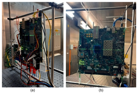
Previous neutron radiation experiments on a ZCU102 board (revision – engineering sample 1) showed that some onboard voltage regulators are vulnerable to high-current events [26]. To protect the board from these anticipated events, we adopted the solution of David S. Lee et al. [26]. Specifically, we 1) removed all onboard voltage regulators for 3.3V (VCC3v3, UTIL_3V3), 0.85V (VCCBRAM, VCCINT, VCCPSINTFP, VCCPSINTLP), 1.2V (DDR4_DIMM_VDDQ) and 1.8V (VCCAUX, VCCOPS) power rails and 2) provided voltage to the mentioned power rails via a multichannel PSU. A Python script running on a PC (see Control-PC in Figure 2) monitored the current drawn from each PSU channel to power cycle (i.e., turn off and on) the board during high-current events. Figure 1(a) shows the ZCU102 board with its voltage rails (0.85V, 1V2, 1V8 and 3V3) powered by an external PSU.
Out-of-the-box ZCU102 board
During the preparation of the tests, before the radiation experiments, we observed that the modified board often crashed during the boot time of the Linux OS (i.e., for testing the LFRiC, SVO and AMD DPU applications). The crashes were caused by voltage droops due to an instantaneous (fast) increase of the current at the 0.85V and 1.2V power rails when the Linux kernel was performing the initialisation of the PS DDR memory. Our external PSU setup could not sustain a stable 0.85V and 1.2V power supply during these current spikes. To overcome the mentioned problem, we ran the Linux-based applications (i.e., complex tests) on the out-of-the-box board. We used the PMBUS Maxim Integrated PowerTool as suggested by [26] to detect SELs. Please note that depending on the target IC, a SEL can cause a rapid increase in the current of a power rail that is difficult to detect on time and power of the device before it is damaged. However, as shown in [26], the rate at which current increases in the XCZU9EG power rails during an SEL is slow. This gives plenty of time (commonly a few minutes) to detect and recover a high-current event by power cycling the target board. Although detecting and recovering a high-current event is faster with an external PSU, the experience we gained from these experiments indicates that the PMBUS Maxim Integrated PowerTool is a sufficient solution to protect the board. Figure 1(b) shows the unmodified ZCU102 board we used for the complex tests.
IV Basic Tests
This section presents the experimental methodology and results of all basic tests. The objectives of these tests are the following: 1) characterise the NSEU and SEFI static cross-sections of all PL memories using synthetic HW benchmarks and 2) evaluate the dynamic SDC and crash cross-sections of several SW-only single-threaded baremetal applications running on the APU.
Experimental setup and overview for all basic tests:
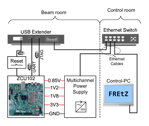
Figure 2 presents the setup for the basic tests, which are conducted on the modified ZCU102 board (see section III-C). Specifically, a computer, namely the Control-PC, is located in the control room and orchestrates the tests by performing the following tasks:
-
•
Configures, controls and monitors the execution of benchmarks on the target board.
-
•
Resets the board during benchmark timeouts (i.e., radiation-induced events that make the device unresponsive) by electrically shorting the board’s SRTS_B and POR_B reset buttons via a USB-controlled relay.
-
•
Monitors an Ethernet-interfaced multichannel PSU to power cycle the board during, if any, high-current events.
Note that all USB connections are transferred from the beam room to the control room via an Ethernet-based USB extender.
IV-A HW-only PL synthetic benchmark tests
Benchmark details
We performed the PL tests on a highly utilised and densely routed design, which instantiates all slice, Block-RAM (BRAM), and Digital Signal Processor (DSP) primitives of the XCZU9EG device. The design has the following characteristics:
-
•
All PL slices are combined into multiple long register chain structures. In detail, the LUTs of SLICEL and SLICEM tiles are configured as route-through and 32-bit Shift Register LUT (SRL), respectively. The LUT outputs of all PL slices are connected with their corresponding slice Flip-Flops (FFs) to form long register chains. Each SRL in the device is initialised with predefined bit patterns.
-
•
All BRAMs are cascaded through their dedicated data bus horizontally (i.e., raw) or vertically (i.e., column) and initialised with address-related bit patterns.
-
•
Clock and clock-enable signals of all BRAM are set to ‘0’ (i.e., disabled) to reduce the likelihood of BRAM upsets caused by Single Event Transients (SETs) on the clock tree and BRAM data bus signals of the device. We aim to reduce transient upsets since we focus on characterising the NSEU and SEFI cross-section of the device.
-
•
All DSP primitives are connected in cascade mode and configured to implement Multiply and ACcumulate (MAC) operations.
Detailed information for the tested synthetic benchmark can be found in our previous work [21], where we used the same benchmark to characterise the PL memories of an AMD Zynq-7000 device under heavy ions.
Testing procedure
The Control-PC downloads via JTAG the bitstream of the PL synthetic benchmark into the XCZU9EG device. In turn, it performs readback capture via JTAG [27] for 50 consecutive times, each time logging the state of all CRAM and Application RAM (ARAM) (e.g., FFs and BRAM contents) bits of the device in a readback file. This test procedure cycle (i.e., one device configuration and 50 readbacks) is continuously performed until the end of the test. In case of an unrecoverable error, the Control-PC performs the following tasks: 1) power cycles the ZCU102 board via the Ethernet-controlled PSU, 2) reconfigures the device and 3) continues readback capture from where it was left before the radiation-induced event occurred. All events that make the XCZU9EG device unresponsive are classified as unrecoverable. For example, a radiation-induced upset in the JTAG circuitry of the target device may result in a connection loss and make the device unresponsive to all JTAG queries made by the Control-PC.
We should make two notes for the testing procedure of the PL synthetic benchmark:
-
•
Accumulated upsets are cleared in the device on average every 1400 seconds, i.e., by downloading the bitstream into the device after 50 continuous readbacks, which last 50 readbacks 28 seconds per readback = 1400 seconds.
-
•
All JTAG transactions with the target device are performed by our open-source FREtZ tool [28, 29]. FREtZ provides a rich set of high-level Python APIs and application examples to readback, verify and manipulate the bitstream and the device state of all AMD 7-series and UltraScale/UltraScale+ MPSoC/FPGAs. Specifically, FREtZ increases the productivity of performing fault-injection and radiation experiments by hiding low-level Vivado TCL/JTAG commands that are executed behind the scenes to access the PS and PL memories of the target device.
-
•
The results of the basic tests are obtained by post-analysis of the collected data (i.e., readback files). Each readback file consists of 1) configuration bits that specify the functionality of the design and device, 2) flip-flop and slice LUTRAM contents, and 3) BRAM contents. Configuration bits are static bits because they do not change during circuit operation, while the flip-flop, LUTRAM, and BRAM contents are dynamic bits, i.e., change during circuit operation, assuming a clock provision. AMD Vivado design suite produces a mask file during bitstream generation that FREtZ applies on each readback file to distinguish the static from the dynamic bits when analysing our experimental data and results.
Results – NSEU cross-section of the PL memories
Table II shows the neutron static cross-section and the number of SEFI occurrences of the target device. Each PL memory type (CRAM, BRAM and SRL) was exposed to radiation for approximately six hours with 5.6E+6 neutrons/cm2/seconds flux, thus accumulating 1.2E+11 neutrons/cm2 fluence on average (see 2nd column of the table). The 1.2E+11 fluence is equivalent to exposing the device to the radiation environment of NYC at sea level for more than 1.3 million hours. In detail, the 3rd column of the table shows the number of upsets for each memory type, while 4th and 5th columns illustrate the cross-section per device and bit, respectively. The CRAM static cross-section that we measured (1.84E-16 cm2/bit) is in the range 1.10 E-16 cm2/bit – 3.40 E-16 cm2/bit as reported in previous studies and summarised in Table I. The cross-section of BRAM and SRL per cm2 per bit is one order of magnitude higher than CRAM, which matches with the findings of AMD [10] and BYU [13].
The last column of Table II shows the number of SEFIs per memory type, which is analysed in the following paragraphs.
| Type | Fluence | NSEU | SEFIs \bigstrut[b] | ||
| Upsets | Cross section | # \bigstrut | |||
| [] | Device | Bit | \bigstrut[t] | ||
| [] | [] | \bigstrut[b] | |||
| CRAM | 1.20E+11 | 2,417 | 2.01E-08 | 1.84E-16 | 0 \bigstrut[t] |
| BRAM | 1.20E+11 | 10,118 | 8.42E-08 | 1.21E-15 | 1 |
| SRL | 1.20E+11 | 1,462 | 1.22E-08 | 1.32E-15 | 1 |
Results – SBU, MBU and MCU events in the PL memories
We adopted the statistical analysis approach of [30] to distinguish NSEUs that caused Single-Bit Upsets (SBUs), Multi-Bit Upsets (MBUs) and Multi-Cell Upsets (MCUs). JEDEC refers to MBUs as multiple upsets occurring in one configuration frame and MCUs expanding in one or more (usually neighbouring) configuration frames [4]. In general, recovering MBUs with classic Error Correction Code (ECC) based CRAM scrubbing[31] is challenging because each configuration frame of the XCZU9EG embeds ECC information that can only support the correction of an SBU. However, ECC scrubbing can successfully correct MCUs (i.e., multiple SBUs in different configuration frames).
Table III presents the percentage of NSEUs that caused an SBU or an MCU, as well as their shapes (i.e., upset patterns). The x-axis of the shapes represents consecutive frames (i.e., frames with consecutive logical addresses), while the y-axis represents consecutive bits in a frame.
Our results show that approximately 96% of NSEUs resulted in SBUs and the remaining 4% in MCUs. The MCUs appear in five shapes as shown in Table III and extend from 2 to 8 frames, while the bit multiplicity reaches up to 3 bits. Finally, we did not observe any MBU, which can be justified by the memory interleaving features of UltraScale/+ MPSoC devices. This is to say, memory cells belonging to the same logically addressed frame are physically separated, thus mitigating MBUs commonly caused in neighbouring physical cells. The NSEU shape results suggest that SECDED scrubbing is an adequate CRAM error recovery mechanism for XCZU9EG MPSoCs used in terrestrial applications since no MBUs were observed during our accelerated radiation tests.
| SBUs [%] | MCUs [%] \bigstrut[t] | ||||
|
|
|||||
| 93.80 | 4.07 | 0.84 | 0.57 | 0.35 | 0.09 \bigstrut[t] |
Results – SEFIs in the PL memories
As shown in Table II we observed two SEFIs during the basic PL tests;
BRAM SEFI: The SEFI exhibited as a multi-bit upset affecting almost all the words of a BRAM. Specifically, all the even-numbered addresses (i.e., 0, 2, …, 1022) of a 36Kb BRAM (i.e., 1024 (32 data bits + 4 parity bits)) were written with the predefined value of the word due to the SEFI, while all the odd-numbered addresses (i.e., 1, 3, …, 1023) were written with the value of the word. This BRAM SEFI resulted in 10.5 kb (instead of 36 kb) upsets since many memory addresses were written with their initial value, i.e., the upsets were logically masked. We excluded the upsets caused by the SEFI when calculating the NSEU cross-section of the BRAMs in Table II.
SRL SEFI: We found that a SET on the clock signal in one CLB slice of an SRL caused the SEFI. Specifically, all the 256 SRL bits located in the eight LUTMs of the same slice (each SLICEM consists of eight 32-bit SRLs, and each SRL occupies a 64-bit LUTM in a master/slave arrangement) were corrupted by the SET on their clock signal. Similarly to the BRAM SEFI, the upsets caused by the SRL SEFI are removed from the NSEU cross-section calculations in Table II.
Results – High-current events in the MPSoC
During the PL tests we observed two high-current events; one occurred at the 1.8V power rail of the MPSoC and one at the 3.3V. The high-current events were successfully recovered by power cycling the device. We did not detect any high-current event in the SW-only single-threaded baremetal benchmarks basic tests and all complex tests.
The results of SEFIs and high-current events show that the probability of such phenomena is extremely low; the device may experience, on average, a BRAM SEFI, a SRL SEFI or two high current events after 1.3 million hours, assuming operation in NYC at sea level. In other words, the equivalent time of natural neutron exposure in NYC to achieve the fluence of the accelerated radiation tests.
IV-B SW-only single-threaded baremetal benchmarks basic tests
Benchmarks details
We executed the following six embedded microprocessor benchmark kernels used in many real-world applications: CRC32, FFT, Qsort, BasicMath, SHA, and MatrixMul. All benchmarks were sourced from the MiBench suite [32], except MatrixMul, which was developed in-house. MiBench programs were adapted to run on the ARM CPU as baremetal single-threaded applications.
We selected or modified the benchmark’s input data sets to compose programs with different memory footprints, i.e., different data memory segment lengths. In this way, we were able to evaluate the impact per cache level on the SDC and crash rates under different cache utilisation conditions. The memory footprints of the benchmarks are shown in Table IV. The data segment includes global and static variables, while Read Only (RO) data includes constant data. One note should be made for the data segment usage of SHA and MatrixMul benchmarks; the SHA and MatrixMul benchmarks have been developed as functions and do not use global and static variables as other benchmarks do. Therefore, all computations for SHA and MatrixMul are performed in local variables. The data segments (stored temporarily in the stack) of the SHA and MatrixMul benchmarks are less than 32 KB and are not reported in Table IV.
In summary, the benchmarks have the following characteristics:
-
•
The data segments of the FFT, BasicMath, SHA and MatrixMul fit into the L1 data cache (32 KB) of the APU core. Thus cache conflict misses are unlikely to happen.
-
•
The data segment of Qsort does not fit into the L1 data cache (32 KB), but it does fit into the L2 cache (1 MB); this means that during the execution of QSort, several conflict cache misses and thus cache replacements may occur in the L1 cache but not in the L2 cache.
-
•
The data segment of CRC32 does not fit into the L2 cache; this means that during the execution of CRC32, several replacements in L2 may occur.
Testing procedure
The Control-PC shown in Figure 2 communicates with the PS through the PL JTAG interface. The PS stores the benchmark output results in the PS DDR memory, and the Control-PC collects the results through the JTAG interface. In more detail, a JTAG-to-AXI bridge is instantiated into the PL to access the DDR memory through a high-performance AXI port. The Control-PC uses the same JTAG-to-AXI bridge interface to configure the PS and initiate the execution of the benchmarks. To guard these auxiliary components (e.g., JTAG-to-AXI bridge) against radiation-induced errors during the tests: 1) we instantiated the AMD SEM IP core [19] to correct CRAM upsets, and 2) triplicated all components (including the SEM IP) in the PL with Synopsis Synplify Premier [33].
| Benchmark | Code Segment | RO Data | Data Segment |
|---|---|---|---|
| FFT | 2.81 KB | 0.20 KB | 2.09 KB |
| SHA | 2.14 KB | 2.32 KB | 0.00 KB |
| BasicMath | 2.74 KB | 0.10 KB | 6.09 KB |
| MatrixMul | 0.77 KB | 23.74 KB | 0.00 KB |
| Qsort | 0.25 KB | 512.00 KB | 156.25 KB |
| CRC32 | 0.57 Kb | 0.00 KB | 2675.56 KB |
Results – SDC and crash cross-sections of the SW-only single-threaded baremetal benchmark basic tests
Table V shows the estimated SDC cross-sections of the single-threaded baremetal benchmarks. Each benchmark ran more than 67k times, resulting in 3 hours of irradiation time per benchmark. The total beam time and fluence for all benchmarks were 18 hours and 6.12E+10 , respectively. Please note that we discarded the overhead time required to configure and initialise the MPSoC and collect the results from the DDR memory.
As expected, all benchmarks with a small memory footprint have either zero (see FFT, BasicMath, MatrixMul) or very low (see SHA) dynamic cross-sections. In contrast, the benchmarks with a large memory footprint (see QSort, CRC32) have the highest cross-section. We observe that Qsort is more vulnerable to SDCs than CRC32 despite its lower data segment size. This can be explained by the higher residence time of its data in the L2 cache. The data segment of Qsort fits in the 1 MB L2 cache of the APU and thus is not updated frequently from the off-chip DDR memory during execution, as done in the case of the CRC32 benchmark. In contrast to the results of [13], we report on average one order of magnitude higher dynamic cross-section for the single-threaded baremetal benchmarks; we tested the MPSoC on a broader range of benchmarks than [13], which exercised the APU caches in a more exhaustive way, thus revealing more errors. As mentioned, the authors in [13] did not observe any SDC or crash but assumed one single error when calculating the dynamic cross-sections of single-threaded baremetal benchmarks running on the APU. However, we did not observe any processor crash, i.e. our findings in regards to the crash dynamic cross-section of the APU are the same as in [13].
| Benchmark | Execution | Fluence | Total | SDC | SDCs |
|---|---|---|---|---|---|
| time (s) | () | runs | cross-section | ||
| FFT | 1,227.95 | 6.96E+09 | 67,509 | 0 | - |
| SHA | 1,239.14 | 7.02E+09 | 67,787 | 2 | 2.85E-10 |
| BasicMath | 1,266.74 | 7.18E+09 | 67,940 | 0 | - |
| MatrixMul | 1,556.26 | 8.82E+09 | 69,406 | 0 | - |
| Qsort | 1,237.92 | 7.01E+09 | 67,487 | 38 | 5.42E-09 |
| CRC32 | 4,269.89 | 2.42E+10 | 67,572 | 18 | 7.44E-10 |
| Total | 10,797.90 | 6.12E+10 | 407,701 | 58 | 9.48E-10 |
V Complex Tests
This section presents the experimental methodology and results of the complex tests. These tests include two SW-only multi-threaded applications and one HW-SW co-design executing a CNN model, all running on top of the Linux OS.
Experimental setup
Testing procedure
The Control-PC runs an in-house developed software, namely the Experiment Control Software (ECS), to orchestrate the test procedure of the target benchmarks through TCP/IP Ethernet.
The ECS software coordinates the tests of the applications via a shared Network File System (NFS) folder as follows: 1) the ECS initially resets the board and waits for it to boot, 2) after a successful OS boot, a bash script running on the MPSoC, namely, the run.sh, executes the following sub-tasks: 3a) connects on the shared NFS folder located on the Control-PC, 3b) updates a sync.log file in the NFS folder to notify the ECS of a successful OS boot, 3c) executes an initial run of the target benchmark to warm-up the CPU caches, 3d) notifies the ECS software via the sync.log file that it is ready to start running the benchmark, 3e) enters an infinite loop where it continuously runs the benchmark and stores the results in the NFS folder to be checked by the ECS. The execution and result checking (i.e., by the ECS) of each benchmark is synchronised with the ECS via a shared mutex.log file stored in the NFS folder. The ECS resets the board when it detects: 1) a boot timeout, 2) a critical error (classifying an error as critical depends on the benchmark characteristics, as shown in the next section), or 3) a result query timeout. It is worth noting that for each benchmark execution, the run.sh script saves the Linux dmesg.log of the target board for post-analysis to identify system-level errors, such as L1 and L2 cache errors (see section V-B).
V-A SW-only multi-threaded applications running under Linux OS
Benchmark details
We tested two SW-only multi-threaded applications, namely the LFRic [22] and the SVO [23], both running on top of the 4.19 Linux kernel, which was configured and compiled with PetaLinux 2019.2.
The LFRic is a weather and climate model and one of the H2020 EuroEXA project (http://euroexa.eu) target applications being developed by the UK’s Met Office and its partners [22]. Much of the LFRic model’s runtime consists of compute-intensive operations suitable for acceleration using FPGAs. The LFRic weather and climate model is based on the GungHo dynamical core with its PSyclone software technology [34]. In our experiments, we exploited an essential computation kernel among the entire LFRic code, the matrix-vector product, to assess the overall dependability (i.e., dynamic cross-section) of the MPSoC. Specifically, this kernel supports 40-bit double-precision floating-point matrix-vector multiplications with an 8 6 matrix and contributes significantly to the execution time of the Helmholtz solver that is used to compute atmospheric pressure [22].
The SVO (Semi-direct Monocular Visual Odometry) processes raw data captured from visual sensors (e.g., camera) and conducts a probabilistic state estimation [23]. In particular, in the probabilistic state estimation, the algorithm calculates the camera’s pose (i.e., motion estimation) and maps it to the surrounding, unknown environment (i.e. mapping). Both operations, the motion estimation and mapping are executed in parallel. SVO is used in many applications such as robotics and automotive applications to implement algorithms involving tasks like ego-motion or pose estimation of objects [23].
Results – Error cross-sections of the SW-only multi-threaded applications
| Benchmark | LFRic | SVO |
| Total runs | 509 | 1,784 |
| Exec. time (hours) | 4.3 | 6.5 |
| Soft-persistent crashes | 6 | 39 |
| Recoverable crashes | 20 | 94 |
| Total crashes | 26 | 133 |
| Tolerable SDCs | 0 | 51 |
| Critical SDCs | 2 | 0 |
| Total SDCs | 2 | 51 |
| Fluence (n/) | 9.35E+10 | 1.29E+11 |
| Total crash cross-section | 2.78E-10 | 1.03E-09 |
| Total SDC cross-section | 2.14E-11 | 3.96E-10 |
Table VI summarises the experimental results of the SW-only multi-threaded Linux-based benchmarks, which were collected during an 11-hour beam session.
We categorise radiation-induced errors as crashes and SDCs. Crashes are further classified into soft-persistent and recoverable errors. Soft-persistent errors require several resets or a device power cycle to bring the MPSoC to a functional state. Recoverable errors require only one device reset to regain functionality. Similarly, SDC errors are classified into critical and tolerable as done in [35]. Critical errors lead to a result out of application specifications. Tolerable errors do not affect the final application result.
Opposite to [13], which did not identify any SDC or processor hang (i.e., crash) when the APU was running multithreaded Linux-based benchmarks, our results showed that the MPSoC can experience radiation-induced errors. In detail, 5.11% and 7.46% of the total runs resulted in a crash for LFRic and SVO, respectively. From the total crashes of LFRiC, 23% were soft-persistent, and 77% were recoverable. For SVO, 29% were soft-persistent and the remaining recoverable.
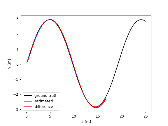
Regarding SDC errors, 0.39% and 2.86% of the total LFRic and SVO runs resulted in SDCs, respectively. However, our findings show that all SDCs of the SVO were tolerable and did not affect the correctness of the final application result. This can be justified by the inherent error resilience nature of computer vision algorithms like SVO, which commonly tolerate most SDCs. In other words, most SDCs cause a small deviation from the ground truth and, therefore, can be ignored. Figure 3 shows the absolute trajectory error of an SVO run under a tolerable SDC error. Although the result (i.e., estimated trajectory) deviated from the ground truth, it did not impact the in-field operation of SVO. On the contrary, all SDCs for the LFRic application affected its final result and therefore were classified as critical. Commonly, the algorithmic nature of LFRic cannot tolerate any SDC.
V-B SW/HW multi-threaded co-design application running under Linux OS
This section includes results for the SW/HW co-design DPU from our previous study [36]. We extend the study by providing the dynamic cross-section of crashes (i.e., hung) as well as the MTTF (see section VI) of the DPU application for different environments and device deployments.
Benchmark details
We tested the MPSoC when running the resnet50 image classification CNN model on the SW/HW Vitis AI DPU co-design. AMD has introduced a rich ecosystem of tools and IP accelerator cores to ease the development of AI applications. In more detail, AMD provides the Vitis AI development environment that encompasses 1) AI frameworks (e.g., Tensorflow), 2) pre-optimised AI models, 3) quantisation and model compression tools, and 4) the DPU with all necessary Linux drivers to seamlessly deploy a CNN application on AMD Zynq-7000 SoC and Zynq UltraScale+ MPSoC devices [37].
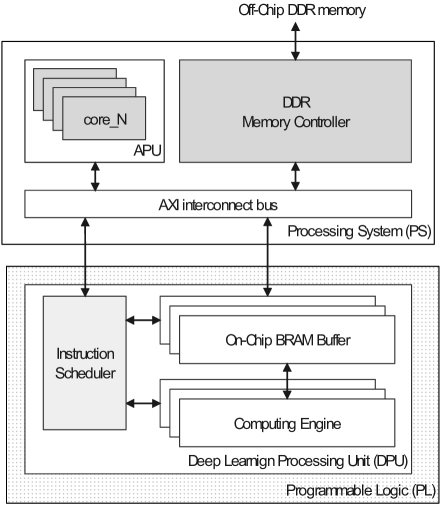
The DPU accelerator is implemented with PL and is tightly interconnected via AXI interfaces to the PS, as shown in Figure 4. The DPU executes special instructions that are generated by the Vitis AI compiler. A typical Vitis AI development flow involves 1) the optimisation and compilation of a CNN model to DPU instructions and 2) the compilation of software running on the APU. The APU pre- and post-processes DNN data controls the DPU and orchestrates the movement of instructions and data between the DPU, the APU and the off-chip DDR memory.
The DPU consists of an instruction scheduler and up to three on-chip BRAM buffers and computing engines. The instruction scheduler fetches and decodes DPU instructions from off-chip memory and controls the on-chip memories and computing engines. The DPU is available in eight architecture configurations, i.e., B512, B800, B1024, B1152, B1600, B2304, B3136, and B4096. Each configuration utilises a different number of computing engines and on-chip memories to target different-size devices and support various DPU functionalities, e.g., ReLU, RELU6, or Leaky-ReLU.
We implemented the Vivado DPU targeted reference design (TRD) [24] provided by Vitis AI v1.3.1 with Vivado 2020.2 for our target board (i.e., ZCU102). The DPU was synthesised with default settings, i.e., B4096 convolution architecture with RAM_USAGE_LOW, CHANNEL_AUGMENTATION_ENABLE, DWCV_ENABLE, POOL_AVG_ENABLE, RELU_LEAKYRELU_RELU6, and Softmax. The parallelism of the DPU can be defined in three dimensions, input channel parallelism (ICP), output channel parallelism (OCP), and pixel parallelism (PP). The B4096 architecture has ICP and OCP equal to 16, PP equal to 8, and can achieve up to 4096 operations per clock cycle. The RAM_USAGE_LOW configuration utilises 257 BRAM36 primitives for buffering weights, bias and intermediate features. Channel augmentation improves the DPU utilisation when the number of input channels is much lower than the available channel parallelism. DepthwiseConv (DWCV), AveragePool, LEAKYRELU and RELU6 are standard CNN parameters that are described in [37]. The design was implemented with Vivado’s Performance_ExplorePostRoutePhysOpt run strategy because Vivado’s default run strategy resulted in time violations for the default operating frequencies of the implemented TRD. Table VII shows the resource utilisation and operating frequency of the DPU TRD. Vivado reported that 41.45% (i.e., 59,281,993 bits) of the device’s configuration bits were essential. Please recall that essential bits are configuration bits that, when corrupted, can potentially cause functional errors in the application.
| Resource | Utilisation | Available | Utilisation | Frequency |
| LUT | 108,208 | 274,080 | 39.48 % | 325 MHz |
| LUTRAM | 11,960 | 144,000 | 8.31 % | 325 MHz |
| FF | 203,901 | 548,160 | 37.20 % | 325 MHz |
| BRAM | 522 | 912 | 57.24 % | 325 MHz |
| DSP | 1,395 | 2,520 | 55.36 % | 650 MHz |
| IO | 7 | 328 | 2.13 % | 325 MHz |
| BUFG | 6 | 404 | 1.49 % | 325 MHz |
| MMCM | 1 | 4 | 25.00 % | 325 MHz |
| PLL | 1 | 8 | 12.50 % | 325 MHz |
| APU | 1 | 1 | 100.00 % | 1200 MHz |
| DDR ctrl. | 1 | 1 | 100.00 % | 533 MHz |
Two important notes can be made for Table VII. First, all resources in the DPU operate at 325 MHz except for the DSPs, which run at 2 325 MHz = 650 MHz. This is because the DPU design applies a double data rate technique on DSP resources. Since DSPs can operate at a much higher frequency than other PL resources, one can perform N times more computation by running the DSPs with N times the frequency of the surrounding logic while multiplexing and de-multiplexing their input and output data, respectively.
Second, the design utilises 319, 55, 405, 4 and 1 LUT, LUTRAM, FF, BRAM and DSP more primitives than the baseline TRD design. This is because we included the AMD SEM IP in the design to perform fault injection and validate our experimental setup before the radiation experiments. However, we turned scrubbing off (configured SEM IP to IDLE mode) during beamtime to allow the DPU to accumulate at least one CRAM upset per image classification. Otherwise, the DPU would have performed almost all classifications without a CRAM upset. The SEM IP operating at 200MHz would have recovered much faster CRAM upsets (1700 upsets per minute) than they occurred (8 upsets per minute – estimated for the 5.6E+6 neutrons/cm2/seconds neutron flux at ChipIR facilities). Instead of scrubbing the device, all CRAM upsets recovered after a device reset when the DPU reported a tolerable or non-tolerable error or a crash (i.e., timeout).
We used Petalinux 2020.2 to generate a Linux OS image for the ZCU102 by using the default Board Support Package (BSP) provided by the DPU-TRD, except 1) the nfs_utils package, which was additionally enabled to mount an NFS folder on Linux, and 2) the u-boot bootloader configuration which mounted an EXT4 file system on an SD card instead of an INITRD RAM disk on the DDR memory.
The CNN application that ran on the DPU was the 8-bit quantised, not pruned resnet50.xmodel, provided by the Vitis AI TRD.
Results – Neutron error (SDC and crash) cross-sections of AMD Vitis DPU running image classification
Table VIII shows the dynamic cross-section of the DPU running the resnet50 image classification CNN for a total fluence of 5.5x10¹⁰ neutrons/cm2 during a 3-hour radiation test session. The DPU accelerator performed 5985 classification runs in total, from which 50% of the runs resulted in an SDC, 1.5% in a crash, and 49.5% were correct. Only 1.57% of the total SDCs resulted in image misclassification or, in other words, were critical. The experimental results show a reliable operation of the DPU even though it did not incorporate any soft error masking scheme in its PL logic like triple modular redundancy (TMR) [38] or ECC in its utilised BRAMs [39].
However, the dynamic cross-section of the DPU is not only affected by soft errors in its PL part but also due to errors in the APU. As mentioned, the DPU is an SW/HW co-design, which means that both the APU and PL logic should cooperate in a reliable manner to successfully classify an image when running the resnet50 model. In the following, we measure the effectiveness of all soft-error mitigation schemes embedded in the APU to cope with upsets in the L1 and L2 caches of the processor.
| Classification | Cross | Conf. Level | |||
|---|---|---|---|---|---|
| runs | Section | 95% | |||
| # | % | (cm2) | Lower | Upper | |
| Correct runs | 2964 | 49.52% | - | - | - |
| Crashes | 89 | 1.49% | 1.60E-09 | 1.26E-09 | 2.02E-09 |
| Critical (C) | 46 | 0.77% | 8.29E-10 | 6.07E-10 | 1.11E-09 |
| Tolerable (T) | 2886 | 48.22% | 5.20E-08 | 5.01E-08 | 5.39E-08 |
| C+T errors | 2932 | 49.99% | 5.28E-08 | 5.09E-08 | 5.48E-08 |
Results – MPSoC APU L1 and L2 cache cross-section when running image classification with the AMD Vitis DPU
We post-processed the Linux dmesg.log files captured during the AMD DPU tests to analyse the NSEUs observed in the MPSoC APU caches. We report the cross-sections of Level-1 Data (L1-D) and Instruction (L1-I) caches, Translation Lookaside Buffer (TLB), Snoop Control Unit (SCU), and Level-2 cache. Moreover, the upsets in the data and tag arrays in both the L1 and L2 caches have been separately identified.
In detail, Table IX shows the dynamic cross-sections of the 32 KB L1-D cache, the 32 KB L1-I cache, and the TLB – a two-level TLB with 512 entries that handles all translation table operations of the APU.
| Size | Upsets | Cross-sec. | Conf. Level 95% | ||
|---|---|---|---|---|---|
| (bit) | (bit) | (cm2/bit) | Lower | Upper | |
| L1-D Data | 262,144 | 32 | 2.20E-15 | 1.50E-15 | 3.11E-15 |
| L1-D Tag | 155,648 | 3 | 3.47E-16 | 7.16E-17 | 1.02E-15 |
| L1-D Total | 417,792 | 35 | 1.51E-15 | 1.05E-15 | 2.10E-15 |
| L1-I Data | 262,144 | 25 | 1.72E-15 | 1.11E-15 | 2.54E-15 |
| L1-I Tag | 147,456 | 4 | 4.89E-16 | 1.33E-16 | 1.25E-15 |
| L1-I Total | 409,600 | 29 | 1.28E-15 | 8.54E-16 | 1.83E-15 |
| L1 TLB | 16,384 | 9 | 9.90E-15 | 4.53E-15 | 1.88E-14 |
| Size | Upsets | Cross-sec. | Conf. Level 95% | ||
|---|---|---|---|---|---|
| (bit) | (bit) | (cm2/bit) | Lower | Upper | |
| L2 Data | 8,388,608 | 293 | 6.29E-16 | 5.59E-16 | 7.06E-16 |
| L2 Tag | 4,194,304 | 20 | 8.59E-17 | 5.25E-17 | 1.33E-16 |
| L2 Total | 12,582,912 | 313 | 4.48E-16 | 4.00E-16 | 5.01E-16 |
| SCU | 155,648 | 4 | 4.63E-16 | 1.26E-16 | 1.19E-15 |
Table X presents the cross-sections of the 1 MB Level-2 cache (L2) and the SCU. The SCU has duplicate copies of the L1 data-cache tags. It connects the APU cores with the device’s accelerator coherency port (ACP) to enable hardware accelerators in the PL to issue coherent accesses to the L1 memory space. The cross-sections of the tag arrays have been calculated based on the tag sizes of the caches, e.g., a 16-bit tag in the 16-way set associative, 64-byte line, 1 MB L2 cache. As mentioned, the cross sections have been calculated for a total fluence of 5.55x10¹⁰ neutrons/cm2. The results show that the cross-sections of the tag arrays are slightly lower than those of the data arrays. The average cross-section calculations for all caches (i.e., L1 and L2) in the MPSoC are close to those reported by Jordan D. Anderson et al. in [13].
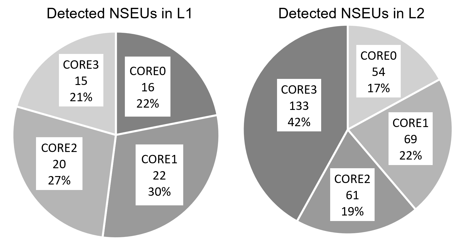
Figure 5 presents the number of detected upsets per cache per APU core. The upsets in the L1 caches are balanced between the four cores, while in the L2 cache, more upsets were observed in the 3rd APU core of the MPSoC. We assume that the Linux OS utilised more Core-3, and thus more cache upsets were detected for Core-3 in the L2 cache.
The private L1-I caches are protected against NSEUs with parity checking (i.e., only error detection is supported), while the private L1-D caches and the shared L2 cache feature SECDED via ECC. However, we observed crashes and SDCs during image classifications with the DPU (and also in the SW-only basic and complex tests) despite the soft error mitigation mechanisms incorporated in the APU caches. We reason that the application errors occurred due to uncorrectable errors in the APU caches (e.g., double-bit errors within a memory word slice of the L1 or L2 caches protected by the same parity bits) or due to upsets in the configuration bits of the PL in case of the DPU. For example, SBUs in L1-D and L2 caches are successfully detected and corrected through SECDED mechanisms, while SBUs in L1-I caches are detected through parity checking and repaired by invalidating and reloading the cache. Similarly, double-bit upsets in L2 are detected by the SECDED scheme and corrected with cache invalidation to force a cache update from a lower memory hierarchy, e.g., DDR. However, if a double-bit error affects a “dirty” line of a write-back L1-D and L2 cache, its data is lost, resulting in data corruption. In case of double-bit upsets in the parity-protected L1-I caches, these cannot be detected.
VI Accessing the reliability of the MPSoC
In sections IV&V, we calculated the static and dynamic cross sections of the XCZU9EG in various scenarios under neutron accelerated radiation testing, e.g., when executing a simple SW-only baremetal single-threaded benchmark or complex Linux-based SW/HW co-design application for image classification. In this section, we project the measured cross-sections of the XCZU9EG at different terrestrial radiation environments and device deployments and examine the reliability of the MPSoC-based computing system under the lens of the MTTU and MTTF dependability metrics as described in section II-B.
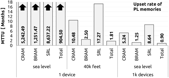
Figure 6 (a) shows the MTTU of the MPSoC’s PL memories assuming 1) a computing system that uses one MPSoC and operates at NYC sea level (e.g., an automotive application), 2) at 40k feet altitude (e.g., avionics), and 3) a system that uses 1k MPSoC devices and operates at the NYC sea level (e.g., a 1000 MPSoC node data centre).
On average, the system consisting of one MPSoC and operating at sea level will experience a neutron-induced upset in the CRAM, BRAM or SRL memories of the device every 904 months (i.e., 75 years). However, the MTTU (i.e. upset rate) of the PL memories of the same system operating at 40k feet altitude drops to 1.81 months (i.e., 500X reduction). On the other hand, a system consisting of 1k MPSoC computing nodes will collectively encounter one upset in PL memories every 0.9 months on average. The MTTU results show that fault-tolerance techniques such as configuration memory scrubbing and ECC in BRAMs should be considered in MPSoC systems that operate at high altitudes or on a large scale (i.e., data centres) to avoid the accumulation of upsets in its PL memories.
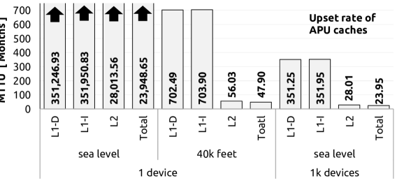
Figure 6 (b) illustrates the MTTU of the L1-D, L1-I and L2 caches of the MPSoC’s APU when running the SW/HW DPU co-design. In other words, the cache upset rates of the APU were calculated by using the dynamic cross-section of caches in the DPU application. As expected, the MTTU of the APU caches is 26.5x higher than the PL memories due to their much smaller size. We calculated that the MTTU of caches in the one- and 1k-node(s) system could drop to 48 and 24 months, respectively, which points out that the parity and SECDED mechanisms of the APU are a necessary feature in the MPSoC, especially when used in large scale systems. The effectiveness of these embedded soft-error mitigation mechanisms is evaluated in the following sections, where we measure the dynamic cross-section of various MPSoC applications, i.e., report the rate at which memory upsets could not be recovered, thus resulting in an SDC or processor crash.
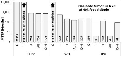
Our analysis shows that the MPSoC has a low upset rate in PL memories and even lower in APU caches when operating in a single node computing system in NYC at sea level and increases in systems operating at high altitudes or on a large scale. In the following, we present the MTTF of MPSoC applications operating in a relatively high neutron flux to understand how an increased upset rate can affect reliability at the application level. In detail, Figure 7 presents the MTTF of the MPSoC when running the SW-only multi-threaded applications (i.e., LFRic and SVO) and the SW/HW DPU co-design. The MTTF of all applications is calculated assuming operation in NYC at 40k feet altitude. However, the MTTF figures for operation at the sea level or for the 1000-node MPSoC system can be calculated by dividing and multiplying the MTTF figures of Figure 7 by 500, respectively.
As mentioned in section V, errors of the complex tests have been categorised into critical SDCs (C), tolerable SDCs (T), and processor hang (H) or otherwise crash. An application failure occurs during an SDC or a processor hang event. In this case, the overall FIT rate of the system is
| (3) |
However, in error-resilient applications, we can omit the from our calculations since tolerable SDCs do not affect output correctness. Thus, the overalls FIT can be calculated as follows:
| (4) |
In Figure 7 the MTTF of is refered as All and for as C+H.
Regarding the MTTF results, we see that the failure rate of the SW-only LFRiC and SVO applications is, on average, one order of magnitude lower than the rate of upsets in APU L2 caches. This shows that the embedded SECDED mechanisms in the APU are effective even for a high upset rate in caches. Although the upset rate in the caches has been calculated for the DPU SW/HW co-design, we believe similar figures would hold for the LFRiC and SVO applications. All complex tests share the same operating system and use the same software to send and receive data from the control PC. Therefore we expect that the caches would be exercised similarly in all benchmarks and thus have the same dynamic cross-section. However, the MTTFAll of SVO is 79% lower than LFRiC, because SVO is more vulnerable to cache upsets due to its larger memory footprint. On the other hand, as mentioned in section V-A, all SDCs in LFRic are critical, while in SVO tolerable. Thus, the reliability degradation of SVO w.r.t. to LFRiC can be limited to 70% if we omit the FIT rate of tolerable SDCs from SVO, i.e. if we consider the MTTFC+H of the applications.
Comparing the SW/HW co-design (i.e., DPU) with the SW-only applications (i.e., BareC, LFRic, and SVO), we observe that the DPU has, on average, 90x lower MTTFAll. This can be justified due to the high FIT rate (low MTTF) of the PL accelerator, which deteriorates the total MTTF of the SW/HW co-design application. In contrast, BareC, LFRic, and SVO do not integrate any PL accelerator and therefore have an overall higher MTTF than the DPU.
However, the MTTFAll of the DPU is very low due to the increased rate of tolerable SDCs. Omitting the FIT rate of tolerable SDCs yields an MTTFC+H = 87 months, which is 4x lower than the MTTFC+H of the SW-only applications. The MTTF results of the DPU show that deploying SW/HW co-design applications at high altitudes or on a large scale requires some form of soft error mitigation like configuration memory scrubbing or even hardware redundancy in high-reliability systems.
VII Conclusions
This article evaluated the neutron Single Event Effect (SEE) sensitivity of the AMD UltraScale+ XCZU9EG MPSoC through accelerated neutron radiation testing and dependability analysis. The cross sections of the device’s Programmable Logic (PL) and Processing System (PS) memories were characterised under the following workloads: 1) a synthetic design that utilised all PL resources, 2) several single-threaded baremetal SW-only benchmarks, 3) two SW-only multi-threaded Linux-based applications for weather prediction and pose estimation, and 4) a SW/HW DPU co-design running the resnet50 image classification model. The device’s neutron CRAM static cross-section was measured to be 1.84E-16cm2/bit, which is in the range of previous studies (1.10E-16 cmcm2/bit – 3.40E-16 cmcm2/bit). The cross-sections of BRAM and SRL memories were one order of magnitude higher than CRAM. No NSEU in the CRAM resulted in a Multi-Cell Upset (i.e., two or more upsets in one configuration frame), concluding that SECDED scrubbing is adequate to recover PL upsets in XCZU9EG devices when used in terrestrial applications. We observed only one BRAM SEFI, one SRL SEFI and two SELs during the accelerated radiation tests, which exposed the MPSoC to more than 1.3 million hours of equivalent natural neutron fluence at NYC sea level. We conclude that the probability of SEFIs and SELs in MPSoC terrestrial applications is extremely low.
To put the cross-section measurements into context, we conducted a dependability analysis assuming a one-node MPSoC system operating at NYC sea level (e.g., automotive) or 40k altitude (e.g., avionics) and a 1000-node MPSoC system at NYC sea level. All SW-only benchmarks achieved a MTTF higher than 148 months in the one-node system at 40k altitude, which points out that the PS can operate reliably despite a relatively high rate of cache upsets (MTTU = 48 months). Thus, we conclude that the embedded SECDED mechanisms of the PS can effectively recover NSEUs even in high altitude or large-scale MPSoC systems. However, the DPU application was more prone to neutron-induced errors than the SW-only workloads. The MTTF of the DPU was estimated to be 4 months, assuming it runs on the same one-node system at sea level. Thus, we conclude that SW/HW applications require extra soft error mitigation, e.g., hardware redundancy, to improve reliability in particular environments and device deployments. Finally, we showed that error-resilient applications like the DPU image classification can ignore tolerable errors to improve MTTF since these do not affect the final system result.
References
- [1] V. Boppana, S. Ahmad et al., “UltraScale+ MPSoC and FPGA families,” in IEEE Hot Chips 27 Symposium (HCS), 2015, pp. 1–37. [Online]. Available: https://doi.org/10.1109/HOTCHIPS.2015.7477457
- [2] A. M. Keller and M. J. Wirthlin, “The Impact of Terrestrial Radiation on FPGAs in Data Centers,” ACM Trans. Reconfigurable Technol. Syst., vol. 15, no. 2, dec 2021. [Online]. Available: https://doi.org/10.1145/3457198
- [3] D. Agiakatsikas, E. Cetin, and O. Diessel, “FMER: An Energy-Efficient Error Recovery Methodology for SRAM-Based FPGA Designs,” IEEE Transactions on Aerospace and Electronic Systems, vol. 54, no. 6, pp. 2695–2712, 2018. [Online]. Available: https://doi.org/10.1109/TAES.2018.2828201
- [4] JEDEC Solid State Technology Association, Measurement and Reporting of Alpha Particle and Terrestrial Cosmic Ray-Induced Soft Errors in Semiconductor Devices (JESD89B - Revision of JESD89A, October 2006), 2021. [Online]. Available: https://www.jedec.org/system/files/docs/JESD89B.pdf
- [5] European Space Components Coordination (ESCC), Single event effects test method and guidelines, ESCC Basic Specification No. 25100, October 2014.
- [6] W. Yang, Y. Li et al., “Atmospheric neutron single event effect test on Xilinx 28 nm system on chip at CSNS-BL09,” Microelectronics Reliability, vol. 99, pp. 119–124, 2019. [Online]. Available: https://doi.org/10.1016/j.microrel.2019.05.004
- [7] S. Mukherjee, Architecture Design for Soft Errors. Morgan Kaufmann, 2011. [Online]. Available: https://doi.org/10.1016/b978-0-12-369529-1.x5001-0
- [8] C. Hu and S. Zain, NSEU Mitigation in Avionics Applications. Application Note (XAPP1073), Xilinx Inc., 2010.
- [9] C. Cazzaniga, M. Bagatin et al., “First Tests of a New Facility for Device-Level, Board-Level and System-Level Neutron Irradiation of Microelectronics,” IEEE Transactions on Emerging Topics in Computing, vol. 9, no. 1, pp. 104–108, 2021. [Online]. Available: https://doi.org/10.1109/TETC.2018.2879027
- [10] P. Maillard, M. Hart et al., “Neutron, 64 MeV Proton & Alpha Single-event Characterization of Xilinx 16nm FinFET Zynq©UltraScale+TM MPSoC,” in IEEE Radiation Effects Data Workshop (REDW), 2017, pp. 1–5. [Online]. Available: https://doi.org/10.1109/NSREC.2017.8115449
- [11] AMD-Xilinx Inc., Device reliability report user guide v10.16 – Second Half 2021 (UG116), 2022.
- [12] C. Johansson and T. Månefjord, “Characterization and Considerations for Upset in FPGA,” in IEEE Nordic Circuits and Systems Conference (NORCAS): NORCHIP and International Symposium of System-on-Chip (SoC), 2018, pp. 1–4. [Online]. Available: https://doi.org/10.1109/NORCHIP.2018.8573506
- [13] J. D. Anderson, J. C. Leavitt, and M. J. Wirthlin, “Neutron Radiation Beam Results for the Xilinx UltraScale+ MPSoC,” in IEEE Radiation Effects Data Workshop (REDW), 2018, pp. 1–7. [Online]. Available: https://doi.org/10.1109/NSREC.2018.8584297
- [14] A. Lesea, W. Koszek et al., “Soft error study of ARM SoC at 28 nanometers,” in Proceeding of the IEEE Workshop on Silicon Errors in Logic-System Effects, 2014, pp. 1–4.
- [15] A. Sari, D. Agiakatsikas, and M. Psarakis, “A soft error vulnerability analysis framework for Xilinx FPGAs,” in Proceedings of ACM/SIGDA International Symposium on Field-programmable Gate Arrays (FPGA). ACM, 2014, pp. 237–240. [Online]. Available: https://doi.org/10.1145/2554688.2554767
- [16] F. Cappello, G. Al et al., “Toward Exascale: 2014 Update,” Supercomput. Front. Innov.: Int. J., vol. 1, no. 1, p. 5–28, apr 2014. [Online]. Available: https://doi.org/10.14529/jsfi140101
- [17] C. Bobda, J. M. Mbongue et al., “The Future of FPGA Acceleration in Datacenters and the Cloud,” ACM Trans. Reconfigurable Technol. Syst., vol. 15, no. 3, feb 2022. [Online]. Available: https://doi.org/10.1145/3506713
- [18] P. Maillard, J. Arver et al., “Test Methodology & Neutron Characterization of Xilinx 16nm Zynq® UltraScale+TM Multi-Processor System-on-Chip (MPSoC),” in IEEE Radiation Effects Data Workshop (REDW), 2018, pp. 1–4. [Online]. Available: https://doi.org/10.1109/NSREC.2018.8584299
- [19] Xilinx Inc., Soft error mitigation controller product guide v4.1 (PG036), April 2018.
- [20] D. S. Lee, M. King et al., “Single-Event Characterization of 16 nm FinFET Xilinx UltraScale+ Devices with Heavy Ion and Neutron Irradiation,” in IEEE Radiation Effects Data Workshop (REDW), 2018, pp. 1–8. [Online]. Available: https://doi.org/10.1109/NSREC.2018.8584313
- [21] V. Vlagkoulis, A. Sari et al., “Single Event Effects Characterization of the Programmable Logic of Xilinx Zynq-7000 FPGA Using VeryUltra High-Energy Heavy Ions,” IEEE Transactions on Nuclear Science (TNS), vol. 68, no. 1, pp. 36–45, 2021. [Online]. Available: https://doi.org/10.1109/TNS.2020.3033188
- [22] M. Ashworth, G. D. Riley et al., “First Steps in Porting the LFRic Weather and Climate Model to the FPGAs of the EuroExa Architecture,” Sci. Program., vol. 2019, Jan 2019. [Online]. Available: https://doi.org/10.1155/2019/7807860
- [23] C. Forster, M. Pizzoli, and D. Scaramuzza, “SVO: Fast semi-direct monocular visual odometry,” in IEEE International Conference on Robotics and Automation (ICRA), 2014, pp. 15–22. [Online]. Available: https://doi.org/10.1109/ICRA.2014.6906584
- [24] “Zynq UltraScale MPSoC DPU TRD V3.3 Vivado 2020.2,” AMD Inc. [Online]. Available: https://github.com/Xilinx/Vitis-AI/blob/v1.3.1/dsa/DPU-TRD/prj/Vivado/README.md
- [25] C. Cazzaniga, R. G. Alía et al., “Study of the Deposited Energy Spectra in Silicon by High-Energy Neutron and Mixed Fields,” IEEE Transactions on Nuclear Science, vol. 67, no. 1, pp. 175–180, 2020. [Online]. Available: https://doi.org/10.1109/TNS.2019.2944657
- [26] D. S. Lee, M. King et al., “Single-event characterization of 16 nm FinFET Xilinx UltraScale+ devices with heavy ion and neutron irradiation,” in IEEE Radiation Effects Data Workshop (REDW), 2018, pp. 1–8. [Online]. Available: https://doi.org/10.1109/NSREC.2018.8584313
- [27] Xilinx Inc., Configuration readback capture in UltraScale FPGAs application note v1.1 (XAPP1230), 2015.
- [28] University of Piraeus - Embedded Systems Lab, “FREtZ (FPGA Reliability Evaluation through JTAG).” [Online]. Available: https://github.com/unipieslab/FREtZ
- [29] A. Sari, V. Vlagkoulis, and M. Psarakis, “An open-source framework for Xilinx FPGA reliability evaluation,” in Proc. Workshop Open Source Design Autom.(OSDA), 2019, pp. 1–6. [Online]. Available: https://osda.gitlab.io/19/3.2.pdf
- [30] M. Wirthlin, D. Lee et al., “A Method and Case Study on Identifying Physically Adjacent Multiple-Cell Upsets Using 28-nm, Interleaved and SECDED-Protected Arrays,” IEEE Transactions on Nuclear Science, vol. 61, no. 6, pp. 3080–3087, 2014. [Online]. Available: https://doi.org/10.1109/TNS.2014.2366913
- [31] A. Saleh, J. Serrano, and J. Patel, “Reliability of scrubbing recovery-techniques for memory systems,” IEEE Transactions on Reliability, vol. 39, no. 1, pp. 114–122, 1990. [Online]. Available: https://doi.org/10.1109/24.52622
- [32] M. Guthaus, J. Ringenberg et al., “MiBench: A free, commercially representative embedded benchmark suite,” in Proceedings of the Fourth Annual IEEE International Workshop on Workload Characterization. WWC-4 (Cat. No.01EX538), 2001, pp. 3–14. [Online]. Available: https://doi.org/10.1109/WWC.2001.990739
- [33] Synopsis Inc., FPGA design solution for high-reliability applications, 2015.
- [34] S. Adams, R. Ford et al., “LFRic: Meeting the Challenges of Scalability and Performance Portability in Weather and Climate Models,” J. Parallel Distrib. Comput., vol. 132, no. C, p. 383–396, oct 2019. [Online]. Available: https://doi.org/10.1016/j.jpdc.2019.02.007
- [35] F. Libano, B. Wilson et al., “Selective Hardening for Neural Networks in FPGAs,” IEEE Transactions on Nuclear Science, vol. 66, no. 1, pp. 216–222, 2019. [Online]. Available: https://doi.org/10.1109/TNS.2018.2884460
- [36] D. Agiakatsikas, N. Foutris et al., “Evaluation of the Xilinx Deep Learning Processing Unit under Neutron Irradiation,” in 21th European Conference on Radiation and Its Effects on Components and Systems (RADECS), 2021, pp. 1–4. [Online]. Available: https://doi.org/10.1109/RADECS53308.2021.9954522
- [37] “Zynq DPU v3.2 Product Guide (UG338),” AMD Inc., July 2020.
- [38] F. P. Mathur and P. T. de Sousa, “Reliability Models of NMR Systems,” IEEE Transactions on Reliability, vol. R-24, no. 2, pp. 108–113, 1975. [Online]. Available: https://doi.org/10.1109/TR.1975.5215106
- [39] J. G. Dobbins, “Error-correcting-code memory reliability calculations,” IEEE Transactions on Reliability, vol. 35, no. 4, pp. 380–384, 1986. [Online]. Available: https://doi.org/10.1109/TR.1986.4335477