Eur. Phys. J. Appl. Phys. 98, 39 (2023)
Atomic relaxation and electronic structure in twisted bilayer MoS2 with rotation angle of 5.09 degrees
Abstract
It is now well established theoretically and experimentally that a moiré pattern, due to a rotation of two atomic layers with respect to each other, creates low-energy flat bands. First discovered in twisted bilayer graphene, these new electronic states are at the origin of strong electronic correlations and even of unconventional superconductivity. Twisted bilayers (tb) of transition metal dichalcogenides (TMDs) also exhibit flat bands around their semiconductor gap at small rotation angles. In this paper, we present a DFT study to analyze the effect of the atomic relaxation on the low-energy bands of tb-MoS2 with a rotation angle of 5.09∘. We show that in-plane atomic relaxation is not essential here, while out-of-plane relaxation dominates the electronic structure. We propose a simple and efficient atomic model to predict this relaxation.
pacs:
PACS-keydiscribing text of that key and PACS-keydiscribing text of that key1 Introduction
The broad family of transition metal dichalcogenides (TMDs) Wang15_reviewTMD ; Liu15_reviewTMD ; Duong17_review offers the possibility to stack two layers with a small angle of rotation to each other, thus forming a moiré pattern superstructure. These twisted bilayers have given rise to numerous experimental vanderZande14 ; Liu14 ; Huang14 ; Huang16 ; Zhang17 ; Trainer17 ; Yeh16 ; Lin18 ; Pan18 ; Zhang20_tTMDC and theoretical Roldan14b ; Fang15 ; Cao15 ; Wang15 ; Constantinescu15 ; Tan16 ; Lu17 ; Naik18 ; Conte19 ; Maity19 ; Tang20 ; Wu20 ; Lu20 ; Pan20 ; Venky20 ; Zhan20 ; Zhang20 ; Naik20 ; Xian21 ; Vitale21 ; Angeli21 ; He21 studies to understand electronic states that are confined by a moiré pattern in semiconductor materials. Many of these studies analyze the interlayer distances, the possible atomic relaxation, the transition from a direct band gap in the monolayer system to an indirect band gap in bilayer systems, and more generally the effect of interlayer coupling in these twisted bilayer 2D systems at various rotation angles . For small values of , the emergence of flat bands has been established from first-principles density functional theory (DFT) calculations Naik18 ; Naik20 and tight-binding (TB) calculations Venky20 ; Zhan20 ; Zhang20 in twisted bilayer MoS2 (tb-MoS2), and observed in a 3∘ twisted bilayer WSe2 sample by using scanning tunneling spectroscopy Zhang20_tTMDC . It has been also shown numerically Lu20 that Lithium intercalation in tb-MoS2 increases interlayer coupling and thus promotes flat bands around the gap. There is also experimental evidence that moiré patterns may give rise to confined states due to the mismatch of the lattice parameters in MoS2–WSe2 heterobilayers Pan18 .
Most theoretical investigations of the electronic structure of bilayer MoS2 are density-functional theory (DFT) studies vanderZande14 ; Liu14 ; Huang14 ; Zhang17 ; Roldan14b ; Fang15 ; Cao15 ; Wang15 ; Constantinescu15 ; Huang16 ; Tan16 ; Lu17 ; Trainer17 ; Naik18 ; Naik20 ; Debbichi14 ; Tao14 ; He14 ; sun2020effects with eventually a Wannier wave function analysis Fang15 . To provide systematic analysis as a function of the rotation angle , in particular for small angles, i.e., very large moiré pattern cells for which DFT calculations are not feasible, several TB models, based on Slater-Koster (SK) parameters Slater54 , have been proposed for monolayer MoS2 Cappelluti13 ; Rostami13 ; Zahid13 ; Ridolfi15 ; SilvaGuillen16 and multi-layer MoS2 Cappelluti13 ; Roldan14b ; Fang15 ; Zahid13 ; Zhan20 ; Zhang20 . Following these efforts, we have proposed Venky20 a SK-TB set of parameters for non-relaxed structures, i.e., rigidly twisted bilayers, that match correctly the DFT bands around the gap of tb-MoS2 with rotation angles . This SK-TB model, with the same parameters, is then used for smaller angles in order to describe the states confined by the moiré pattern. For , the valence band with the highest energy is separated from the other valence states by a minigap of a few meV. In addition, the width of this band decreases as decreases so that the average velocity of these electronic states reaches 0 for such that almost flat bands emerge at these angles. This is reminiscent of the vanishing of the velocity at certain “magic” rotation angles in twisted bilayer graphene Trambly10 ; SuarezMorell10 ; Bistritzer11 . However, in bilayer MoS2 it arises for an interval of angles and not a set of specific values. Other minigaps and flat bands are also found in the conduction band. The confined states that are closest to the gap are localized in the AA stacking regions of the moiré pattern, as in twisted bilayer graphene. However, for small angles, it has been shown Naik18 ; Naik20 ; Vitale21 that atomic relaxation strongly modifies these low-energy bands, in particular their approximate degeneracy. A better understanding of atomic relaxation and its effects on the electronic structure is therefore essential not only for very small angles but also for larger ones ().
In this paper, we present a DFT study of tb-MoS2 with a rotation angle of . This angle is approximately the angle below which the highest energy valence band (just below the gap) is isolated from the rest of the valence states by a minigap for non-relaxed structures. We show that, unlike the case of very small angles Naik18 ; Naik20 ; Vitale21 , atomic relaxation amounts to essentially out-of-plane atomic displacements along the -direction that can be simulated simply as a function of the atomic positions in the moiré cell. This simple atomic model allows to understand the origin of the modifications of the electronic structure induced by the relaxation.
2 Structure and DFT calculations
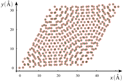
The construction of the commensurable twisted bilayer we study is explained in detail in Refs. Venky20 ; Venky_these . It corresponds to with 762 atoms per unit cell. Starting from an AA stacked bilayer (where Mo atoms of a layer lie above a Mo atom of the other layer, and S atoms of a layer lie above an S atom of the other layer), one layer (layer “”) is rotated with respect to the other layer (layer “”) by the angle around an axis containing two Mo atoms. Thus, AA stacking regions are located at the corner of the moiré cell (Fig. 1(bottom)). BA’ stacking regions (where S atoms lie above a Mo, and Mo (S) do not lie above any atom of layer (layer )), and AB’ stacking regions (regions where Mo lie above an S, and S (Mo) do not lie above any atom of layer (layer )) are located at and of the long diagonal of the moiré cell, respectively.
The DFT calculations were carried out with the ABINIT software Gonze02 ; Gonze09 ; Gonze16 . We have checked previously Venky20 ; Venky_these that LDA Jones89 and GGA Perdew96 + Van der Waals exchange-correlation functionals yield very similar results, so all the results presented here are based on LDA calculations, which require less computation time for large systems. While the results presented here may not be quantitatively very accurate, they are sufficient to qualitatively show the importance of out-of-plane atomic displacements on the electronic structure of the low-energy flat bands. Likewise, the exact value of the band gap may not be very precise in LDA, but the evolution of this gap and the existence of minigaps are significant. The Brillouin zone was sampled by a k-point mesh in reciprocal space within the Monkhorst-Pack scheme Monkhorst76 . One k-point is used for atomic relaxation and a 22 k-grid for the self-consistency procedure of the electronic structure calculation. The kinetic energy cutoff was chosen to be 408 eV. We checked that a 33 k-grid for the self-consistency procedure and an energy cutoff of 544.22 eV yield very similar bands for the relaxed structure. The structural optimization of atomic positions is done by using the Broyden-Fletcher-Goldfarb-Shanno minimization. A vacuum region of 10 Å was inserted between the MoS2 bilayers to avoid spurious interactions between periodic images. In our calculations, the spin-orbit coupling (SOC) is not taken into account in order to reduce the calculation time. SOC is important for TMDs, as it introduces some band splittings close to the gap Ridolfi15 ; SilvaGuillen16 ; Naik18 ; Zhan20 ; He21 , however it will not change the existence or not of low-energy flat bands in tb-MoS2, so it is not essential for the present study.
3 Atomic relaxation
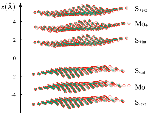
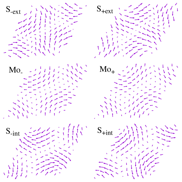
The DFT-relaxed atomic structure of tb-MoS2 with rotation angle is shown in Fig. 1. Remarkably, the in-plane displacement of each atom with respect to the rigidly twisted structure is rather small. Indeed, the average is Å, Å, and Å, for atoms S±ext, Mo±, and S±int, respectively. Such displacements are almost not visible in Fig. 1(bottom), and they have little effect on the electronic structure (see next section). This result shows that the strong in-plane displacements obtained for the smallest angles Naik18 ; Naik20 ; Vitale21 are not too important for . However, it is interesting to note that these small displacements are precursors to the larger displacements and shear solitons obtained for the smallest angles Naik18 , as shown in Fig. 2. These in-plane displacements tend to reduce the AA stacking regions with respect to the AB stacking regions to minimize the energy Naik18 ; Naik20 ; Vitale21 .
| Structure | S±ext | Mo± | S±int | |
|---|---|---|---|---|
| non-relaxed | ||||
| relaxed | ||||
| -mod | ||||
| bilayer AA | ||||
| bilayer AB’ (BA’) | ||||
On the other hand, the displacements along the -direction are important. For each atomic layer, the mean values of the -coordinate and the corresponding standard deviation are given in Table 1. As expected given the interplane distances in the simple stacking cases (see Ref. He14 and Table 1), the distance between layers is greater in the AA stacking regions than in AB’ (BA’) stacking regions. Inspired by the work of Koshino et al. Koshino18 for twisted bilayer graphene, we propose the following atomic model (“-mod” model) where in-plane atomic coordinates are those of the rigidly twisted bilayer and the modulation of the atomic -coordinates are calculated by
| (1) |
where are the non-relaxed positions of the atoms in the rigidly twisted moiré cell, and are the six vectors of the reciprocal lattice that define the first Brillouin zone of the moiré pattern. For each atomic layer, i.e., for the six Mo and S atomic layers of tb-MoS2, and are the values of the DFT-relaxed structure at (AA stacking region) and at AB’ or BA’ stacking regions (Table 1). Figure 1 shows that DFT-relaxed positions and -mod positions fit well together.
4 Electronic band dispersion
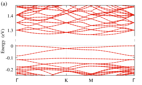


The DFT band dispersions are shown for the DFT-relaxed bilayer and the rigidly twisted bilayer (non-relaxed bilayer) in Fig. 3(a) and 3(b), respectively. For the non-relaxed bilayer the interlayer distance is that obtained for simple AA stacking, like in our previous calculations Venky20 . In the non-relaxed tb-MoS2, the minimum of the conduction band is at K like for monolayer MoS2, which is no longer the case after atomic relaxation. Fig. 3(c) shows a zoom of the highest-energy valence bands. The relaxation does not change the valence band maximum energy at K. However it leads to significant modifications of the bands close to the gap. For the non-relaxed structure Venky20 , when , the highest-energy band is non-degenerate and isolated from the other valence bands by a minigap. For , this minigap is equal to meV (Fig. 3(c)). For the relaxed structure there is no isolated single valance band, but 2 bands which cross in K while remaining linear in (around K). This result is similar to that of Naik et al. Naik18 ; Naik20 and Vitale et al. Vitale21 , obtained by using a multiscale approach, a pair potential for relaxation, and DFT or TB calculations for the band dispersion. There are nevertheless small differences. For instance, in our calculation, the bandwidth for these first two valence bands is 84 meV with respect to meV in Ref. Naik20 . Unlike that previous calculation, these two bands are isolated from the rest of the valence bands by a minigap of meV.
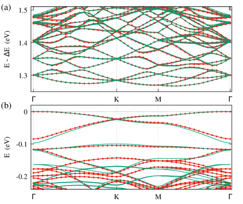
To test the validity of the structure with the -modulation only (Eq. (1)), bands around the gap of DFT-relaxed and -mod structures are compared in Fig. 4. The gaps of the two structures are slightly different (difference of 36 meV), which may be due to the difference between the average values per atomic layer (Table 1). The conduction bands are nevertheless almost the same and valence bands are very similar. In particular, the two valence bands closest to the gap that are characteristic of the atomic relaxation effect are well reproduced. Therefore, the simplified relaxation model given by formula (1) is sufficient to account for the low-energy flat bands due to a moiré pattern at not too small rotation angles.
5 Conclusion
We have performed a DFT study of the atomic relaxation and the electronic band dispersion of twisted bilayer MoS2 with a rotation angle equal to . Contrary to what has been observed for very small angles (typically less than ) Naik18 ; Naik20 ; Vitale21 , the in-plane atomic displacements with respect to a rigidly twisted bilayer are very small, and they have almost no effect on band dispersion. However, the out-of-plane displacements are large and significantly alter the low-energy bands around the gap. These atomic displacements can be modeled by a simple formula that depends only on the interlayer distances in the AA and AB stacking regions.
The reduction of bandwidth and related emergence of flat bands identifies weakly doped MoS2 bilayers as good candidates for the observation of strong correlation effects. For a complete theoretical study of electronic correlations in these complex systems, it is important to take into account the atomic relaxation. We offer here a simple out-of-plane atomic displacements model for not too small rotation angles, typically a few degrees. Preliminary investigations (not shown here) indicate that for determining the electronic structure of low-energy bands, the Slater-Koster tight-binding models Venky20 ; Zhan20 , that are efficient for rigidly twisted bilayers, would require a further adjustment of the parameters in order to be applicable to the -modulated structures.
6 Acknowledgments
Calculations have been performed at the Centre de Calcul (CDC), CY Cergy Paris Université, and at GENCI-IDRIS (Grant No. A0060910784). We thank Y. Costes and B. Mary, CDC, for computing assistance. This work was supported by the ANR project FlatMoi (ANR-21-CE30-0029) and the Paris//Seine excellence initiative (Grants No. 2017-231-C01-A0 and AAP2019-0000000113).
7 Authors contributions
S. Venkateswarlu, A. Misssaoui, and G. Trambly de Laissardière performed the DFT calculations and the numerical analysis. S. Venkateswarlu, A. Honecker, and G. Trambly de Laissardière wrote and revised the manuscript. All authors discussed the results and approved the final version of the manuscript.
References
- (1) H. Wang, H. Yuan, S. Sae Hong, Y. Li, Y. Cui, Chem. Soc. Rev. 44, 2664 (2015)
- (2) G.B. Liu, D. Xiao, Y. Yao, X. Xu, W. Yao, Chem. Soc. Rev. 44, 2643 (2015)
- (3) D.L. Duong, S.J. Yun, Y.H. Lee, ACS Nano 11, 11803 (2017)
- (4) A.M. van der Zande, J. Kunstmann, A. Chernikov, D.A. Chenet, Y. You, X. Zhang, P.Y. Huang, T.C. Berkelbach, L. Wang, F. Zhang et al., Nano Letters 14, 3869 (2014)
- (5) K. Liu, L. Zhang, T. Cao, C. Jin, D. Qiu, Q. Zhou, A. Zettl, P. Yang, S.G. Louie, F. Wang, Nat. Commun. 5, 4966 (2014)
- (6) S. Huang, X. Ling, L. Liang, J. Kong, H. Terrones, V. Meunier, M.S. Dresselhaus, Nano Letters 14, 5500 (2014)
- (7) S. Huang, L. Liang, X. Ling, A.A. Puretzky, D.B. Geohegan, B.G. Sumpter, J. Kong, V. Meunier, M.S. Dresselhaus, Nano Letters 16, 1435 (2016)
- (8) C. Zhang, C.P. Chuu, X. Ren, M.Y. Li, L.J. Li, C. Jin, M.Y. Chou, C.K. Shih, Science Advances 3, e1601459 (2017)
- (9) D.J. Trainer, A.V. Putilov, C. Di Giorgio, T. Saari, B. Wang, M. Wolak, R.U. Chandrasena, C. Lane, T.R. Chang, H.T. Jeng et al., Scientific Reports 7, 40559 (2017)
- (10) P.C. Yeh, W. Jin, N. Zaki, J. Kunstmann, D. Chenet, G. Arefe, J.T. Sadowski, J.I. Dadap, P. Sutter, J. Hone et al., Nano Letters 16, 953 (2016)
- (11) M.L. Lin, Q.H. Tan, J.B. Wu, X.S. Chen, J.H. Wang, Y.H. Pan, X. Zhang, X. Cong, J. Zhang, W. Ji et al., ACS Nano 12, 8770 (2018)
- (12) Y. Pan, S. Fölsch, Y. Nie, D. Waters, Y.C. Lin, B. Jariwala, K. Zhang, K. Cho, J.A. Robinson, R.M. Feenstra, Nano Letters 18, 1849 (2018)
- (13) Z. Zhang, Y. Wang, K. Watanabe, T. Taniguchi, K. Ueno, E. Tutuc, B.J. LeRoy, Nature Physics 16, 1093 (2020)
- (14) R. Roldán, J.A. Silva-Guillén, M.P. López-Sancho, F. Guinea, E. Cappelluti, P. Ordejón, Ann. Phys. (Leipzig) 526, 347 (2014)
- (15) S. Fang, R. Kuate Defo, S.N. Shirodkar, S. Lieu, G.A. Tritsaris, E. Kaxiras, Phys. Rev. B 92, 205108 (2015)
- (16) B. Cao, T. Li, J. Phys. Chem. C 119, 1247 (2015)
- (17) Z. Wang, Q. Chen, J. Wang, J. Phys. Chem. C 119, 4752 (2015)
- (18) G.C. Constantinescu, N.D.M. Hine, Phys. Rev. B 91, 195416 (2015)
- (19) Y. Tan, F.W. Chen, A.W. Ghosh, Appl. Phys. Lett. 109, 101601 (2016)
- (20) N. Lu, H. Guo, Z. Zhuo, L. Wang, X. Wu, X.C. Zeng, Nanoscale 9, 19131 (2017)
- (21) M.H. Naik, M. Jain, Phys. Rev. Lett. 121, 266401 (2018)
- (22) F. Conte, D. Ninno, G. Cantele, Phys. Rev. B 99, 155429 (2019)
- (23) I. Maity, P.K. Maiti, H.R. Krishnamurthy, M. Jain, Phys. Rev. B 103, L121102 (2021)
- (24) Y. Tang, L. Li, T. Li, Y. Xu, S. Liu, K. Barmak, K. Watanabe, T. Taniguchi, A.H. MacDonald, J. Shan et al., Nature 579, 353 (2020)
- (25) J. Wu, L. Meng, J. Yu, Y. Li, physica status solidi (b) 257, 1900412 (2020)
- (26) Z. Lu, S. Carr, D.T. Larson, E. Kaxiras, Phys. Rev. B 102, 125424 (2020)
- (27) H. Pan, F. Wu, S. Das Sarma, Phys. Rev. Research 2, 033087 (2020)
- (28) S. Venkateswarlu, A. Honecker, G. Trambly de Laissardière, Phys. Rev. B 102, 081103(R) (2020)
- (29) Z. Zhan, Y. Zhang, P. Lv, H. Zhong, G. Yu, F. Guinea, J.A. Silva-Guillén, S. Yuan, Phys. Rev. B 102, 241106(R) (2020)
- (30) Y. Zhang, K. Jiang, Z. Wang, F. Zhang, Phys. Rev. B 102, 035136 (2020)
- (31) M.H. Naik, S. Kundu, I. Maity, M. Jain, Phys. Rev. B 102, 075413 (2020)
- (32) L. Xian, M. Claassen, D. Kiese, M.M. Scherer, S. Trebst, D.M. Kennes, A. Rubio, Nat. Commun. 12, 5644 (2021)
- (33) V. Vitale, K. Atalar, A.A. Mostofi, J. Lischner, 2D Mater. 8, 045010 (2021)
- (34) M. Angeli, A.H. MacDonald, Proc. Natl. Acad. Sci. USA 118, e2021826118 (2021)
- (35) F. He, J. Li, L. Li, X. Mao, Z. Liu, S. Teng, J. Wang, Y. Wang, Europhys. Lett. 136, 17001 (2021)
- (36) L. Debbichi, O. Eriksson, S. Lebègue, Phys. Rev. B 89, 205311 (2014)
- (37) T. Peng, G. Huai-Hong, Y. Teng, Z. Zhi-Dong, Chinese Physics B 23, 106801 (2014)
- (38) J. He, K. Hummer, C. Franchini, Phys. Rev. B 89, 075409 (2014)
- (39) F. Sun, T. Luo, L. Li, A. Hong, C. Yuan, W. Zhang, Computational Materials Science 188, 110205 (2021)
- (40) J.C. Slater, G.F. Koster, Phys. Rev. 94, 1498 (1954)
- (41) E. Cappelluti, R. Roldán, J.A. Silva-Guillén, P. Ordejón, F. Guinea, Phys. Rev. B 88, 075409 (2013)
- (42) H. Rostami, A.G. Moghaddam, R. Asgari, Phys. Rev. B 88, 085440 (2013)
- (43) F. Zahid, L. Liu, Y. Zhu, J. Wang, H. Guo, AIP Advances 3, 052111 (2013)
- (44) E. Ridolfi, D. Le, T.S. Rahman, E.R. Mucciolo, C.H. Lewenkopf, J. Phys.: Condens. Matter 27, 365501 (2015)
- (45) J.A. Silva-Guillén, P. San-Jose, R. Roldán, Applied Sciences 6, 284 (2016)
- (46) G. Trambly de Laissardière, D. Mayou, L. Magaud, Nano Letters 10, 804 (2010)
- (47) E. Suárez Morell, J.D. Correa, P. Vargas, M. Pacheco, Z. Barticevic, Phys. Rev. B 82, 121407(R) (2010)
- (48) R. Bistritzer, A.H. MacDonald, Proc. Natl. Acad. Sci. USA 108, 12233 (2011)
- (49) S. Venkateswarlu, PhD thesis, CY Cergy Paris Université, Cergy-Pontoise, France (2021), https://tel.archives-ouvertes.fr/tel-03383066
- (50) X. Gonze, J.M. Beuken, R. Caracas, F. Detraux, M. Fuchs, G.M. Rignanese, L. Sindic, M. Verstraete, G. Zerah, F. Jollet et al., Computational Materials Science 25, 478 (2002)
- (51) X. Gonze, B. Amadon, P.M. Anglade, J.M. Beuken, F. Bottin, P. Boulanger, F. Bruneval, D. Caliste, R. Caracas, M. Côté et al., Comp. Phys. Commun, 180, 2582 (2009)
- (52) X. Gonze, F. Jollet, F. Abreu Araujo, D. Adams, B. Amadon, T. Applencourt, C. Audouze, J.M. Beuken, J. Bieder, A. Bokhanchuk et al., Comp. Phys. Commun, 205, 106 (2016)
- (53) R.O. Jones, O. Gunnarsson, Rev. Mod. Phys. 61, 689 (1989)
- (54) J.P. Perdew, K. Burke, M. Ernzerhof, Phys. Rev. Lett. 77, 3865 (1996)
- (55) H.J. Monkhorst, J.D. Pack, Phys. Rev. B 13, 5188 (1976)
- (56) S. Grimme, J. Comput. Chem. 27, 1787 (2006)
- (57) M. Koshino, N.F.Q. Yuan, T. Koretsune, M. Ochi, K. Kuroki, L. Fu, Phys. Rev. X 8, 031087 (2018)