DISS. ETH NO. 28621
IMPROVING DRAM PERFORMANCE, RELIABILITY, AND SECURITY
BY RIGOROUSLY UNDERSTANDING INTRINSIC DRAM OPERATION
A thesis submitted to attain the degree of
DOCTOR OF SCIENCES of ETH ZÜRICH
(Dr. sc. ETH Zürich)
presented by
HASAN HASSAN
B.Sc. & M.Sc., TOBB University of Economics and Technology
born on 4 July 1991
accepted on the recommendation of
Prof. Dr. Onur Mutlu, examiner
Prof. Dr. Derek Chiou, co-examiner
Prof. Dr. Mattan Erez, co-examiner
Dr. Mike O’Connor, co-examiner
Prof. Dr. Moinuddin Qureshi, co-examiner
Dr. Christian Weis, co-examiner
2022
Hasan Hassan: Improving DRAM Performance, Reliability, and Security by Rigorously Understanding Intrinsic DRAM Operation, © 2022
DOI: TBD
To my wife, Seray.
Acknowledgments
I received tremendous help from many people throughout the six years I spent at ETH Zürich.
Foremost, I extend my deepest gratitude to my advisor, Onur Mutlu, for his continuous support and guidance during my PhD journey. Back when I visited his research group at CMU as an intern, his passion in teaching and research was what steered me towards pursuing a PhD degree. As my PhD advisor, he has always been patient with me and provided insightful criticism and advice on my research. Without him, I may not have even attempted to pursue a PhD degree and could not have written this thesis.
I would like to express my sincere gratitude to my PhD committee members, Derek Chiou, Mattan Erez, Mike O’Connor, Moinuddin Qureshi, and Christian Weis, for their time and efforts to review my thesis and provide valuable feedback.
I am grateful to all SAFARI group members for providing stimulating intellectual environment and their friendship. I thank Jeremie Kim and Minesh Patel for their company since my early days at ETH as friends and excellent researchers. Surviving PhD would not be possible without them. I thank the other members of SAFARI, including Giray Yağlıkçı, Can Fırtına, Juan Gómez Luna, Ataberk Olgun, Haocong Luo, Geraldo De Oliveira, Lois Orosa, Nisa Bostancı, Rahul Bera, Yahya Can Tuğrul, Konstantinos Kanellopoulos, Jisung Park, Nika Mansouri Ghiasi, Mohammed Alser, Jawad Haj-Yahya, Arash Tavakkol, Yaohua Wang, Joël Lindegger, Mohammad Sadrosadati, Roknoddin Azizibarzoki, João Ferreira, Christian Rossi, Tracy Ewen, and many others for their collaboration and support.
I am also thankful to wonderful collaborators I had the chance to work with during my PhD. I thank Saugata Ghose for the great assistance he provided during my time at CMU and after. I also thank many others that I met at CMU, including Nandita Vijaykumar, Vivek Seshadri, Samira Khan, Donghyuk Lee, Gennady Pekhimenko, Amirali Boroumand, Kevin Chang, Yixin Luo, Lavanya Subramanian, Rachata Ausavarungnirun, Damla Senol, and Nastaran Hajinazar. I thank Kaveh Razavi for fascinating discussions on various security topics. I thank Victor van der Veen, Pietro Frigo, and Emanuele Vannacci for their contributions. I thank my internship mentors Stephan Meier and Tyler Huberty for their guidance during my time at Apple.
Finally, I would like to thank my family for their endless support, encouragement, and love. I thank my parents, Meryem and Ibrahim, and my sister, Ayşegül, for always standing by me and enabling all this. Above all I would like to thank my wife Seray, who kept me motivated to write this thesis with her unwavering support and love.
Abstract
DRAM is the primary technology used for main memory in modern systems. Unfortunately, as DRAM scales down to smaller technology nodes, it faces key challenges in both data integrity and latency, which strongly affect overall system reliability, security, and performance. To develop reliable, secure, and high-performance DRAM-based main memory for future systems, it is critical to rigorously characterize, analyze, and understand various aspects (e.g., reliability, retention, latency, RowHammer vulnerability) of existing DRAM chips and their architecture. The goal of this dissertation is to 1) develop techniques and infrastructures to enable such rigorous characterization, analysis, and understanding, and 2) enable new mechanisms to improve DRAM performance, reliability, and security based on the developed understanding.
To this end, in this dissertation, we 1) design, implement, and prototype a new practical-to-use and flexible FPGA-based DRAM characterization infrastructure (called SoftMC), 2) use the DRAM characterization infrastructure to develop a new experimental methodology (called U-TRR) to uncover the operation of existing proprietary in-DRAM RowHammer protection mechanisms and craft new RowHammer access patterns to efficiently circumvent these RowHammer protection mechanisms, 3) propose a new DRAM architecture, called Self-Managing DRAM, for enabling autonomous and efficient in-DRAM maintenance operations that enable not only better performance, efficiency, and reliability but also faster and easier adoption of changes to DRAM chips, and 4) propose a versatile DRAM substrate, called the Copy-Row (CROW) substrate, that enables new mechanisms for improving DRAM performance, energy consumption, and reliability.
SoftMC. To develop reliable and high-performance DRAM-based main memory in future systems, it is critical to experimentally characterize, understand, and analyze various aspects (e.g., reliability, latency) of existing DRAM chips. To enable this, there is a strong need for a publicly-available DRAM testing infrastructure that can flexibly and efficiently test DRAM chips in a manner accessible to both software and hardware developers. To this end, we design and prototype SoftMC: a flexible and practical FPGA-based DRAM testing infrastructure. SoftMC implements all low-level DRAM operations (i.e., DDR commands) available in a typical memory controller (e.g., opening a row in a bank, reading a specific column address, performing a refresh operation, enforcing various timing constraints between commands). Using these low-level operations, SoftMC can test and characterize any (existing or new) DRAM mechanism that uses the existing DDR interface. SoftMC provides its users with a simple and intuitive high-level programming interface that completely hides the low-level details of the FPGA. SoftMC is freely available as an open-source tool and it has enabled many research projects since its release, leading to new understanding and new techniques.
U-TRR. RowHammer is a critical vulnerability in modern DRAM chips that can lead to reliability, safety, and security problems in computing systems. As such, DRAM vendors have been implementing techniques to protect DRAM chips against RowHammer. We challenge the claim of DRAM vendors that their DRAM chips are completely protected against RowHammer using proprietary, undocumented, and obscure on-die Target Row Refresh (TRR) mechanisms. To assess the security guarantees of recent DRAM chips, we develop Uncovering TRR (U-TRR), a new experimental methodology to analyze in-DRAM TRR implementations. U-TRR is based on the new observation that data retention failures in DRAM enable a side channel that leaks information on how TRR refreshes potential victim rows. U-TRR allows us to (i) understand how logical DRAM rows are laid out physically in silicon; (ii) study undocumented on-die TRR mechanisms; and (iii) combine (i) and (ii) to evaluate the RowHammer security guarantees of modern DRAM chips. We show how U-TRR allows us to craft RowHammer access patterns that successfully circumvent the TRR mechanisms employed in 45 DRAM modules of the three major DRAM vendors. We find that the DRAM modules we analyze are vulnerable to RowHammer, having bit flips in up to 99.9% of all DRAM rows and that simple error-correcting codes cannot prevent bit flips. As such, more robust techniques to protect against the RowHammer vulnerability are necessary. We publicly release the source code of our implementation of the U-TRR methodology.
Self-Managing DRAM. To ensure reliable and secure DRAM operation, three types of maintenance operations are typically required: 1) DRAM refresh, 2) RowHammer protection, and 3) memory scrubbing. The reliability and security of DRAM chips continuously worsen as DRAM technology node scales to smaller sizes. Consequently, new DRAM chip generations necessitate making existing maintenance operations more aggressive (e.g., lowering the refresh period) and introducing new types of maintenance operations (e.g., targeted refresh for mitigating RowHammer) while keeping the overheads of maintenance operations minimal. Unfortunately, modifying the existing DRAM maintenance operations is difficult due to the current rigid DRAM interface that places the memory controller completely in charge of DRAM control. Implementing new or modifying existing maintenance operations often require difficult-to-realize changes in the DRAM interface, the memory controller, and potentially other system components (e.g., system software). Our goal is to 1) ease, and thus accelerate, the process of implementing new DRAM maintenance operations and 2) enable more efficient in-DRAM maintenance operations. To this end, we propose Self-Managing DRAM (SMD), a new low-cost DRAM architecture that enables implementing new in-DRAM maintenance mechanisms with no further changes in the DRAM interface, memory controller, or other system components. We use SMD to implement six maintenance mechanisms for three use cases: 1) DRAM refresh, 2) RowHammer protection, and 3) memory scrubbing. Our evaluations show that SMD-based maintenance operations have significantly lower system performance and energy overheads compared to conventional DDR4 DRAM. A combination of SMD-based maintenance mechanisms that perform refresh, RowHammer protection, and memory scrubbing achieve significant speedup and lower DRAM energy across a wide variety of system configurations. SMD’s benefits increase as DRAM chips become denser. We publicly release all SMD source code and data.
CROW. Three major challenges to DRAM scaling (i.e., high access latencies, high refresh overheads, and increasing reliability problems like RowHammer) are difficult to solve efficiently by directly modifying the underlying cell array structure. This is because commodity DRAM implements an extremely dense DRAM cell array that is optimized for low area-per-bit. Because of its density, even a small change in the DRAM cell array structure may incur non-negligible area overhead. Thus, we would like to lower the DRAM access latency, reduce the refresh overhead, and improve DRAM reliability with no changes to the DRAM cell architecture, and with only minimal changes to the DRAM chip. To this end, we propose Copy-Row DRAM (CROW), a flexible substrate that enables new mechanisms for improving DRAM performance, energy efficiency, and reliability. We use the CROW substrate to implement 1) a low-cost in-DRAM caching mechanism that lowers DRAM activation latency to frequently-accessed rows by 38% and 2) a mechanism that avoids the use of short-retention-time rows to mitigate the performance and energy overhead of DRAM refresh operations. CROW’s flexibility allows the implementation of both mechanisms at the same time. Our evaluations show that the two CROW-based mechanisms synergistically improve system performance by 20.0% and reduce DRAM energy by 22.3% for memory-intensive four-core workloads. We publicly release the source code of CROW.
Holistically, via these four major contributions, this dissertation shows the importance of rigorously characterizing the reliability, latency, and RowHammer vulnerability of existing DRAM chips and understanding their architecture for developing practical and low-overhead mechanisms for efficiently improving DRAM reliability, security, and performance. We believe and hope that, via the new infrastructure, understanding, and techniques we develop and enable, this dissertation encourages similar experimental understanding-driven innovation in the design of future memories.
Zusammenfassung
DRAM ist die wichtigste Hauptspeicher-Technologie in modernen Systemen. Leider steht DRAM bei der Verkleinerung auf kleinere Technologieknoten vor grossen Herausforderungen in Bezug auf Datenintegrität und Latenz, die die Zuverlässigkeit, Sicherheit und Leistung des Gesamtsystems stark beeinträchtigen. Um zuverlässige, sichere und leistungsstarke DRAM-basierte Hauptspeicher für künftige Systeme zu entwickeln, müssen verschiedene Aspekte (z. B. Zuverlässigkeit, Datenerhaltung, Latenz, RowHammer-Anfälligkeit) der vorhandenen DRAM-Chips und ihrer Architektur genau charakterisiert, analysiert und verstanden werden. Ziel dieser Dissertation ist es, 1) Techniken und Infrastrukturen zu entwickeln, die eine solche rigorose Charakterisierung, Analyse und ein solches rigoroses Verständnis ermöglichen, und 2) neue Mechanismen zur Verbesserung der DRAM-Leistung, -Zuverlässigkeit und -Sicherheit auf der Grundlage des entwickelten Verständnisses zu ermöglichen.
Zu diesem Zweck entwickeln, implementieren und prototypisieren wir in dieser Dissertation 1) eine neue praktisch einsetzbare und flexible FPGA-basierte DRAM-Charakterisierungsinfrastruktur (genannt SoftMC), 2) die DRAM-Charakterisierungsinfrastruktur zur Entwicklung einer neuen experimentellen Methodik (genannt U-TRR) verwendet, um die Funktionsweise bestehender proprietärer In-DRAM RowHammer-Schutzmechanismen aufzudecken und neue RowHammer-Zugriffsmuster zu entwickeln, um diese RowHammer-Schutzmechanismen effizient zu umgehen, 3) eine neue DRAM-Architektur, genannt Self-Managing DRAM, vorschlagen, um autonome und effiziente In-DRAM Wartungsvorgänge zu ermöglichen, die nicht nur eine bessere Leistung, Effizienz und Zuverlässigkeit, sondern auch eine schnellere und einfachere Annahme von Änderungen an DRAM-Chips ermöglichen, und 4) ein vielseitiges DRAM-Substrat, genannt Copy-Row (CROW)-Substrat, vorschlagen, das neue Mechanismen zur Verbesserung der DRAM-Leistung, des Energieverbrauchs und der Zuverlässigkeit ermöglicht.
SoftMC. Für die Entwicklung zuverlässiger und leistungsfähiger DRAM-basierter Hauptspeicher in zukünftigen Systemen ist es von entscheidender Bedeutung, verschiedene Aspekte (z. B. Zuverlässigkeit, Latenz) der vorhandenen DRAM-Chips experimentell zu charakterisieren, zu verstehen und zu analysieren. Um dies zu ermöglichen, besteht ein dringender Bedarf an einer öffentlich zugänglichen DRAM-Testinfrastruktur, mit der DRAM-Chips flexibel und effizient getestet werden können und die sowohl für Software- als auch für Hardware-Entwickler zugänglich ist. Zu diesem Zweck entwickeln und prototypisieren wir SoftMC: eine flexible und praktische FPGA-basierte DRAM-Testinfrastruktur. SoftMC implementiert alle Low-Level-DRAM-Operationen (d.h. DDR-Befehle), die in einem typischen Speicher-Controller verfügbar sind (z.B. Öffnen einer Zeile in einer Bank, Lesen einer bestimmten Spaltenadresse, Durchführen einer Refresh-Operation, Durchsetzen verschiedener Timing-Beschränkungen zwischen Befehlen). Mit diesen Low-Level-Operationen kann SoftMC jeden (existierenden oder neuen) DRAM-Mechanismus, der die existierende DDR-Schnittstelle nutzt, testen und charakterisieren. SoftMC bietet seinen Benutzern eine einfache und intuitive High-Level-Programmierschnittstelle, die die Low-Level-Details des FPGAs vollständig verbirgt. SoftMC ist als Open-Source-Tool frei verfügbar und hat seit seiner Veröffentlichung viele Forschungsprojekte ermöglicht, die zu neuen Erkenntnissen und neuen Techniken geführt haben.
U-TRR. RowHammer ist eine kritische Schwachstelle in modernen DRAM-Chips, die zu Zuverlässigkeits-, Sicherheits- und Schutzproblemen in Computersystemen führen kann. Aus diesem Grund haben DRAM-Hersteller Techniken zum Schutz von DRAM-Chips vor RowHammer implementiert. Wir hinterfragen die Behauptung von DRAM-Anbietern, ihre DRAM-Chips seien durch proprietäre, undokumentierte und undurchsichtige on-die Target Row Refresh (TRR)-Mechanismen vollständig gegen RowHammer geschützt. Um die Sicherheitsgarantien aktueller DRAM-Chips zu bewerten, entwickeln wir Uncovering TRR (U-TRR), eine neue experimentelle Methode zur Analyse von TRR-Implementierungen im DRAM. U-TRR basiert auf der neuen Beobachtung, dass Fehler bei der Datenerhaltung in DRAM einen Seitenkanal ermöglichen, der Informationen darüber preisgibt, wie TRR potenzielle Opfer-Zeilen refresht. U-TRR ermöglicht es uns, (i) zu verstehen, wie logische DRAM-Zeilen physisch in auf dem chip angeordnet sind; (ii) undokumentierte on-die TRR-Mechanismen zu untersuchen; und (iii) Punkte (i) und (ii) zu kombinieren, um die RowHammer-Sicherheitsgarantien moderner DRAM-Chips zu bewerten. Wir zeigen, wie U-TRR es uns ermöglicht, RowHammer-Zugriffsmuster zu erstellen, die erfolgreich die TRR-Mechanismen umgehen, die in 45 DRAM-Modulen der drei großen DRAM-Hersteller eingesetzt werden. Wir stellen fest, dass die von uns analysierten DRAM-Module anfällig für RowHammer sind, da in bis zu 99,9% aller DRAM-Zeilen Bitflips auftreten, und dass einfache Fehlerkorrekturcodes Bitflips nicht verhindern können. Daher werden robustere Techniken zur Verhinderung der RowHammer-Schwachstelle benötigt. Wir veröffentlichen den Quellcode unserer Implementierung der U-TRR-Methode.
Self-Managing DRAM. Um einen zuverlässigen und sicheren DRAM-Betrieb zu gewährleisten, sind in der Regel drei Arten von Wartungsvorgängen erforderlich: 1) DRAM-Refresh, 2) RowHammer-Schutz und 3) Memory-Scrubbing. Die Zuverlässigkeit und Sicherheit von DRAM-Chips verschlechtert sich ständig, da die DRAM-Technologieknoten immer kleiner werden. Folglich müssen bei neuen DRAM-Chip-Generationen die bestehenden Wartungsvorgänge aggressiver gestaltet werden (z. B. Verringerung des Refresh-Periode) und neue Arten von Wartungsvorgängen eingeführt werden (z. B. gezielte Refreshes zur Milderung von RowHammer), während der Overhead der Wartungsvorgänge minimal gehalten wird. Leider ist die Änderung der bestehenden DRAM-Wartungsvorgänge aufgrund der derzeitigen starren DRAM-Schnittstelle, die die DRAM-Steuerung vollständig dem Speicher-Controller überlässt, schwierig. Die Implementierung neuer oder die Änderung bestehender Wartungsvorgänge erfordert häufig schwer zu realisierende Änderungen an der DRAM-Schnittstelle, dem Speicher-Controller und anderen Systemkomponenten (z. B. Systemsoftware). Unser Ziel ist es, 1) den Prozess der Implementierung neuer DRAM-Wartungsvorgänge zu vereinfachen und damit zu beschleunigen und 2) effizientere In-DRAM-Wartungsvorgänge zu ermöglichen. Zu diesem Zweck schlagen wir Self-Managing DRAM (SMD) vor, eine neue, kostengünstige DRAM-Architektur, die die Implementierung neuer In-DRAM Wartungsmechanismen ohne weitere Änderungen an der DRAM-Schnittstelle, dem Speicher-Controller oder anderen Systemkomponenten ermöglicht. Wir verwenden SMD zur Implementierung von sechs Wartungsmechanismen für drei Anwendungsfälle: 1) DRAM-Refresh, 2) RowHammer-Schutz und 3) Memory-Scrubbing. Unsere Auswertungen zeigen, dass SMD-basierte Wartungsvorgänge im Vergleich zu konventionellem DDR4-DRAM eine deutlich geringere Systemleistungs- und Energiekosten haben. Eine Kombination aus SMD-basierten Wartungsmechanismen, die Refresh-, RowHammer-Schutz- und Memory-Scrubbing-Operationen durchführen, führt zu einer erheblichen Beschleunigung und einem geringeren DRAM-Energieverbrauch in einer Vielzahl von Systemkonfigurationen. Die Vorteile von SMD nehmen zu, je dichter die DRAM-Chips werden. Wir veröffentlichen den gesamten SMD-Quellcode und -Daten.
CROW. Die drei grössten Herausforderungen bei der Skalierung von DRAM (d. h. hohe Zugriffslatenzen, hohe Refresh-Kostenund zunehmende Zuverlässigkeitsprobleme wie RowHammer) lassen sich nur schwer durch direkte Änderung der zugrunde liegenden Zell-Array-Struktur effizient lösen. Dies liegt daran, dass handelsüblicher DRAM ein extrem dichtes DRAM-Zellen-Array implementiert, das auf eine geringe Fläche pro Bit optimiert ist. Aufgrund dieser Dichte kann selbst eine kleine Änderung der DRAM-Zellen-Array-Struktur zu einem nicht zu vernachlässigenden Flächen-Overhead führen. Daher möchten wir die DRAM-Zugriffslatenz verringern, die Refresh-Kosten- reduzieren und die DRAM-Zuverlässigkeit verbessern, ohne die DRAM-Zellenarchitektur zu verändern und mit nur minimalen Änderungen am DRAM-Chip. Zu diesem Zweck schlagen wir Copy-Row DRAM (CROW) vor, ein flexibles Substrat, das neue Mechanismen zur Verbesserung der DRAM-Leistung, Energieeffizienz und Zuverlässigkeit ermöglicht. Wir verwenden das CROW-Substrat, um 1) einen kostengünstigen In-DRAM Caching-Mechanismus zu implementieren, der die DRAM-Aktivierungslatenz für häufig genutzte Zeilen um 38% verringert, und 2) einen Mechanismus, der die Verwendung von Zeilen mit kurzer Datenerhaltungsdauer vermeidet, um den Leistungs- und Energie-Overhead von DRAM-Refresh-perationen zu verringern. Die Flexibilität von CROW ermöglicht die gleichzeitige Implementierung beider Mechanismen. Unsere Auswertungen zeigen, dass die beiden CROW-basierten Mechanismen die Systemleistung um 20,0% verbessern und den DRAM-Energieverbrauch bei speicherintensiven Vier-Kern-Workloads um 22,3% senken. Wir veröffentlichen den Quellcode von CROW.
Mit diesen vier Hauptbeiträgen zeigt diese Dissertation, wie wichtig es ist, die Zuverlässigkeit, Latenz und RowHammer-Anfälligkeit bestehender DRAM-Chips genau zu charakterisieren und ihre Architektur zu verstehen, um praktische und kostengünstige Mechanismen zur effizienten Verbesserung der Zuverlässigkeit, Sicherheit und Leistung von DRAM zu entwickeln. Wir glauben und hoffen, dass diese Dissertation durch die neue Infrastruktur, das Verständnis und die Techniken, die wir entwickeln und ermöglichen, ähnliche, auf experimentellem Verständnis beruhende Innovationen bei der Entwicklung zukünftiger Speicher anregt.
?chaptername? 1 Introduction
1.1 Problem Discussion
Dynamic Random Access Memory (DRAM) [4] has long been the dominant memory technology used in almost all computing systems due to its low latency and low cost per bit. DRAM vendors scale the DRAM technology by shrinking DRAM cells to continuously reduce the cost of DRAM [5]. Unfortunately, while the density of the DRAM chips has been increasing as a result of technology scaling, high-density DRAM chips face three critical challenges [6, 5]: (1) high access latencies, (2) high refresh overheads, and (3) increasing reliability problems. These three DRAM scaling challenges have a major impact on the performance, energy, and robustness (i.e., reliability, safety, and security) of a system. We examine each of these critical challenges in turn.
Challenge 1: High Access Latency. The high DRAM access latency is a challenge to improving system performance and energy efficiency. While DRAM capacity increased significantly over the last two decades [7, 8, 9, 10, 2, 11, 6, 5, 12, 13, 14, 15], DRAM access latency decreased only slightly [2, 6, 10, 5, 12, 13, 14, 11, 15, 16, 17]. The high DRAM access latency significantly degrades the performance of many workloads [18, 19, 20, 21, 22, 11, 2, 23, 24, 25, 26, 27, 28, 29, 30, 9, 31, 32, 33, 34, 35, 36]. The performance impact is particularly large for applications that 1) have working sets exceeding the cache capacity of the system, 2) suffer from high instruction and data cache miss rates, and 3) have low memory-level parallelism. While some DRAM vendors offer latency-optimized DRAM modules [37, 38], these modules have significantly lower capacity and higher cost compared to commodity DRAM [2, 39, 3]. Thus, reducing the high DRAM access latency without significantly affecting capacity and cost in commodity DRAM remains an important challenge [23, 2, 5, 6].
Challenge 2: High Refresh Overhead. The high DRAM refresh overhead is a challenge to improving system performance and energy consumption. A DRAM cell stores data in a capacitor that leaks charge over time. To maintain correctness, every DRAM cell requires periodic refresh operations that restore the charge level in a cell. As the DRAM cell size decreases with process technology scaling, newer DRAM devices contain both more DRAM cells and smaller DRAM cells than older DRAM devices [40]. As a result, the performance and energy overheads of refresh operations scale unfavorably as DRAM technology scales into the future [41, 42, 43]. In modern DDR5 [44] devices, the memory controller refreshes every DRAM cell every at the nominal temperature range and every at the extended temperature range. Previous studies show that 1) refresh operations incur large performance overheads, as DRAM cells cannot be accessed when the cells are being refreshed [41, 43, 45, 46, 47, 48, 49, 50, 51, 52, 53, 54, 55, 56, 57, 58, 59, 60]; and 2) a large fraction (e.g., 50% in DRAM chips) of the total DRAM energy is consumed by the refresh operations [43, 41, 49, 47, 57, 56, 59, 60].
Challenge 3: Increasing Reliability Problems. The increasing vulnerability of DRAM cells to various failure mechanisms is an important challenge to maintaining DRAM reliability with a small system performance and energy overhead. As the process technology node size reduces, DRAM cells get smaller and closer to each other, and thus they become more susceptible to failures [61, 5, 62, 63, 64, 43, 65, 66, 67, 68, 69, 6, 70, 71, 72, 73, 74, 75]. A real and prevalent example of such a failure mechanism in modern DRAM is the RowHammer vulnerability [73, 72, 74, 76]. RowHammer causes disturbance errors (i.e., bit flips in vulnerable DRAM cells that are not being accessed) in DRAM rows physically adjacent to a row that is repeatedly activated many times. In addition to being detrimental to DRAM reliability, RowHammer also poses a threat to system security and safety. Prior works [70, 77, 78, 73, 79, 80, 81, 82, 83, 84, 85, 86, 87, 88, 89, 90, 91, 92, 93, 94, 95, 96, 97] propose various mechanisms that protect systems against RowHammer at the cost of increased performance and energy overheads. DRAM also exhibits other reliability issues (e.g., data retention failures, soft errors) that necessitate expensive solutions (e.g., increasing refresh rate, memory scrubbing), which lead to high performance and energy overheads.
Our Goal. To combat the system-level implications of the technology scaling challenges of DRAM, it is essential to rigorously understand DRAM cell behavior and the architecture of existing DRAM chips. The goal of this dissertation is to 1) develop techniques and infrastructures to enable such rigorous characterization, analysis, and understanding, and 2) enable new mechanisms to improve DRAM performance, reliability, and security based on the developed understanding.
To this end, in this dissertation, we first design, implement, and prototype SoftMC, a practical-to-use and flexible FPGA-based DRAM characterization infrastructure. SoftMC enables detailed analyses on DRAM cell characteristics of real DRAM chips via precise control on the low-level DRAM interface. Second, we use SoftMC to uncover the operation and weaknesses of RowHammer protection mechanisms implemented in modern DRAM chips. We develop a methodology (called U-TRR) that uses DRAM retention failures as a side-channel to monitor when a RowHammer protection mechanism performs additional refresh operation to protect DRAM rows susceptible to a RowHammer attack. Based on the understanding we develop, we craft new RowHammer access patterns that efficiently circumvent in-DRAM RowHammer protection mechanisms implemented in modern DDR4 DRAM chips from three major DRAM vendors. Third, we propose Self-Managing DRAM (SMD), a new DRAM architecture and interface to enable in-DRAM maintenance operations to efficiently perform 1) DRAM refresh, 2) RowHammer protection, and 3) memory scrubbing. Our proposal eases the adoption of new DRAM maintenance mechanisms by setting the memory controller free from managing such DRAM maintenance operations. Finally, we propose the Copy-Row (CROW) DRAM substrate that exploits the fast and efficient data movement within a DRAM subarray to enable new mechanisms for improving DRAM performance, energy consumption, and reliability.
1.2 Thesis Statement
Our thesis statement is as follows:
Understanding DRAM characteristics and operation through
rigorous experimentation
using real DRAM chips pave the way for developing
new mechanisms that significantly
improve DRAM performance, energy consumption, reliability,
and security.
1.3 Our Approach
We first enable detailed characterization of modern DRAM chips by designing and prototyping a flexible FPGA-based infrastructure, which we then use to develop understanding and mechanisms for improving system performance, efficiency, reliability, and security. In the remainder of this section, we briefly introduce our DRAM characterization infrastructure, new characterization studies, and new mechanisms.
1.3.1 Infrastructure for Characterizing DRAM Chips
To easily study the reliability characteristics and the operation of real DRAM chips, we design and prototype SoftMC (Soft Memory Controller), a flexible and easy-to-use experimental DRAM testing infrastructure. SoftMC is an FPGA-based DRAM testing infrastructure that exposes the low-level DRAM command interface to its users via a high-level programming interface. The high-level programming interface completely hides the low-level details of the FPGA from users. Users implement their DRAM experiment routines or mechanisms in a high-level language that automatically gets translated into the low-level SoftMC operations in the FPGA. SoftMC offers a wide range of use cases, such as characterizing the effects of variation within a DRAM chip and across DRAM chips, verifying the correctness of new DRAM mechanisms on actual hardware, and experimentally discovering the reliability, retention, and timing characteristics of an unknown or newly-designed DRAM chip (or finding the best specifications for a known DRAM chip). SoftMC was published at HPCA 2017 [1] and released as an open source tool [98] at the same time. Since then, many works [29, 10, 99, 100, 71, 101, 70, 102, 103, 69, 104, 75, 105, 106, 107, 108, 109, 110, 111, 112, 113, 114] used different versions of SoftMC in various DRAM characterization studies as well as studies that introduced new ideas.
1.3.2 Understanding in-DRAM RowHammer Protection Mechanisms
We use SoftMC to study the security guarantees of RowHammer protection mechanisms that DRAM vendors implement in their chips. Different vendors implement different RowHammer protection mechanisms, commonly referred to as Target Row Refresh (TRR). The main idea of TRR is to detect an aggressor row (i.e., a row that is frequently activated within a time frame) and refresh its victim rows (i.e., neighboring rows that are physically adjacent to the aggressor row). However, the exact operation of TRR is unknown. Some of the major DRAM vendors advertise RowHammer-free DDR4 DRAM chips [115, 116, 100]. However, none of the DRAM vendors have so far disclosed the implementation details let alone proved the protection guarantees of their TRR mechanisms. Thus, we need new methods for identifying whether or not DRAM chips are fully secure against RowHammer. We develop U-TRR, a practical methodology that uncovers the inner workings of TRR mechanisms in modern DRAM chips. The goal of U-TRR is to enable the observation (i.e., uncovering) of all protective refreshes generated by TRR after inducing a carefully crafted sequence of DRAM accesses. To make this possible, we make a key observation that retention failures that occur on a DRAM row can be used as a side channel to detect when the row is refreshed, due to either TRR or periodic refresh operations. U-TRR uncovers important details of the TRR designs of three major DRAM vendors. We demonstrate the usefulness of these insights for developing effective RowHammer attacks on DRAM chips from each vendor by crafting specialized DRAM access patterns that hammer a row enough times to cause a RowHammer bit flip without alerting the TRR protection mechanism (i.e., by redirecting potential TRR refreshes away from the victim rows). In our evaluation, we find that all tested DRAM modules with different manufacturing dates (from 2016 to 2020) are vulnerable to the new access patterns we can craft via U-TRR. We open source our U-TRR methodology and make it freely available for further research and development [117].
1.3.3 Enabling Easy Adoption of Efficient in-DRAM Maintenance Operations
We develop a new DRAM architecture and interface, Self-Managing DRAM, to enable autonomous in-DRAM maintenance operations. For reliable and secure operation of modern and future DRAM chips, DRAM maintenance operations, such as periodic refresh, RowHammer protection, and memory scrubbing are critical. An ideal maintenance operation should efficiently improve DRAM reliability and security with minimal system performance and energy consumption overheads. As DRAM technology node scales to smaller sizes, the reliability and security of DRAM chips worsen. As a result, new DRAM chip generations necessitate making existing maintenance operations more intensive (e.g., increasing the refresh rate [44, 118, 80] and memory scrubbing frequency [49]) and introducing new types of maintenance operations (e.g., targeted refresh [103, 100, 119] and DDR5 RFM [44] as RowHammer defenses). Unfortunately, modifying the DRAM maintenance operations is difficult due to the current rigid DRAM interface that places the memory controller completely in charge of DRAM control. Implementing new or modifying existing maintenance operations often require difficult-to-realize changes in the DRAM interface, the memory controller, and other system components (e.g., system software). Self-Managing DRAM 1) eases the process and thus speed of implementing new DRAM maintenance operations and 2) enables more efficient in-DRAM maintenance operations. Using Self-Managing DRAM, we develop maintenance operations for refresh, RowHammer protection, and memory scrubbing that incur significantly lower system performance and energy overhead compared to existing state-of-the-art approaches. We believe that enabling autonomous in-DRAM maintenance operations would encourage innovation, reduce time-to-market, and ease adoption of novel mechanisms that improve DRAM efficiency, reliability, and security. To foster research and development in this direction, we open source our Self-Managing DRAM framework [120] and early-release our Self-Managing DRAM work on arXiv.org [121].
1.3.4 Improving DRAM Access Latency and Reducing DRAM Refresh Overhead via Simultaneous Row Activation
We propose Copy-Row DRAM (CROW), a flexible in-DRAM substrate that can be used in multiple different ways to address the performance, energy efficiency, and reliability challenges of DRAM. The key idea of CROW is to provide a fast, low-cost mechanism to duplicate select rows in DRAM that contain data that is most sensitive or vulnerable to latency, refresh, or reliability issues. At a high level, CROW partitions each DRAM subarray into two regions (regular rows and copy rows) and enables independent control over the rows in each region. Using CROW, we develop two novel mechanisms: 1) CROW-cache, which reduces the DRAM access latency and 2) CROW-ref, which reduces the DRAM refresh overhead. The key idea of CROW-cache is to 1) duplicate data from recently-accessed regular rows into a small cache made up of copy rows, and 2) simultaneously activate a duplicated regular row with its corresponding copy row when the regular row needs to be activated again. By activating both the regular row and its corresponding copy row, CROW-cache reduces the time needed to open the row and begin performing read and/or write requests to the row by 38%. The key idea of CROW-ref is to avoid storing any data in DRAM rows that contain weak cells, such that the entire DRAM chip can use a longer refresh interval. CROW-ref uses an efficient profiling mechanism [122] to identify weak DRAM cells, remaps the regular rows containing weak cells to strong copy rows, and records the remapping information. Our evaluations show that CROW-cache and CROW-ref significantly improve system performance and energy efficiency compared to conventional DRAM and incur small hardware area overhead. We also describe how CROW can be used to mitigate the RowHammer vulnerability. To aid future research and development, we open source CROW [123].
1.4 Contributions
This dissertation makes the following major contributions:
-
1.
We introduce SoftMC, the first open-source FPGA-based experimental memory testing infrastructure. SoftMC implements all low-level DRAM operations in a programmable memory controller that is exposed to the user with a flexible and easy-to-use interface, and hence enables the efficient characterization of modern DRAM chips and evaluation of mechanisms built on top of low-level DRAM operations. To our knowledge, SoftMC is the first publicly-available infrastructure that exposes a high-level programming interface to ease memory testing and characterization.
-
(a)
We provide a prototype implementation of SoftMC with a high-level software interface for users and a low-level FPGA-based implementation of the memory controller. We have released the software interface and the implementation publicly as a freely-available open-source tool [98].
-
(b)
We demonstrate the capability, flexibility, and programming ease of SoftMC by implementing two example use cases. Our first use case demonstrates the ease of use of SoftMC by implementing a routine for retention time characterization of DRAM cells. Our second use case demonstrates the effectiveness of SoftMC as a new tool to test existing or new mechanisms on existing memory chips. Using SoftMC, we demonstrate that the expected effect (i.e., highly-charged DRAM rows can be accessed faster than others) of two recently-proposed mechanisms is not observable in 24 modern DRAM chips from three major vendors.
-
(a)
-
2.
Using SoftMC, we extensively analyze 45 modern DDR4 modules from three major DRAM vendors to understand the operation and security guarantess of their in-DRAM RowHammer protection mechanisms called Target Row Refresh (TRR). We develop U-TRR, a new methodology for reverse-engineering TRR mechanisms and assessing their security properties.
-
(a)
We use U-TRR to understand and uncover the TRR implementations of 45 DDR4 modules from the three major DRAM vendors. This evaluation shows that our new methodology is broadly applicable to any DRAM chip.
-
(b)
Leveraging the TRR implementation details uncovered by U-TRR, we craft specialized RowHammer access patterns that make existing TRR protections ineffective.
-
(c)
Our specialized U-TRR-discovered access patterns are significantly more effective than patterns from the state-of-the-art [100]: we show that our new RowHammer access patterns cause 1) bit flips in all 45 DDR4 modules we comprehensively examine, 2) bit flips in up to 99.9% of the all rows in a DRAM bank, and 3) two and more (up to ) bit flips in a single 8-byte dataword, enabling practical RowHammer attacks in systems that employ ECC.
-
(d)
We release the source code of our U-TRR methodology to aid future research and development [117].
-
(a)
-
3.
We develop Self-Managing DRAM (SMD), a new DRAM chip design and interface to enable autonomous and efficient in-DRAM maintenance operations. We implement SMD with small changes to modern DRAM chips and memory controllers. The core components of SMD incur area overhead of only 1.63% of a DRAM chip and increase DRAM row activation latency by only 0.4%.
-
(a)
We use SMD to implement efficient DRAM maintenance mechanisms for three use cases: periodic refresh, RowHammer protection, and memory scrubbing.
-
(b)
We rigorously evaluate the performance and energy of the new maintenance mechanisms. SMD provides large performance and energy benefits while also improving reliability and security across a variety of systems and workloads.
-
(c)
We open source our Self-Managing DRAM framework to aid future research and development in this direction [120].
-
(a)
-
4.
We introduce Copy-Row DRAM (CROW), a flexible and low-cost substrate in commodity DRAM that enables mechanisms for improving DRAM performance, energy efficiency, and reliability by providing two sets of rows that have independent control in each subarray. CROW does not change the extremely-dense cell array and has low cost (0.48% additional area overhead in the DRAM chip, storage overhead in the memory controller, and 1.6% DRAM storage capacity overhead).
-
(a)
We propose three mechanisms that exploit the CROW substrate: 1) CROW-cache, an in-DRAM cache to reduce the DRAM access latency, 2) CROW-ref, a remapping scheme for weak DRAM rows to reduce the DRAM refresh overhead, and 3) a mechanism for mitigating the RowHammer vulnerability. We show that CROW allows these mechanisms to be employed at the same time.
-
(b)
We evaluate the performance, energy savings, and overhead of CROW-cache and CROW-ref, showing significant performance and energy benefits over a state-of-the-art commodity DRAM chip. We also compare CROW-cache to two prior proposals to reduce DRAM latency [3, 2] and show that CROW-cache is more area- and energy-efficient at reducing DRAM latency.
-
(c)
We make the source code of CROW publicly available to aid future research and development [123].
-
(a)
1.5 Outline
This dissertation consists of 8 chapters. chapter 2 provides background on DRAM organization, operation, and problems, which are essential for understanding our proposals in later chapters. In chapter 3, we describe SoftMC, our new FPGA-based DRAM characterization infrastructure. chapter 4 presents our U-TRR methodology for uncovering the operation of in-DRAM TRR mechanisms using SoftMC. chapter 5 introduces Self-Managing DRAM (SMD), a new DRAM architecture and interface for enabling efficient and autonomous in-DRAM maintenance operations. chapter 6 presents Copy-Row DRAM (CROW), a substrate that makes slight modifications in DRAM subarray architecture to enable efficient mechanisms for improving DRAM performance, energy efficiency, and reliability. Finally, chapter 7 summarizes the dissertation and provides future research directions that this dissertation enables.
?chaptername? 2 Background
In this chapter, we provide the background on DRAM necessary for understanding our methods, observations, and techniques presented in later chapters. We first describe DRAM organization and operation. Afterward, we discuss the major performance, reliability, and security problems of DRAM that we tackle. We refer the reader to many prior works in the area [10, 41, 39, 99, 124, 17, 73, 3, 11, 2, 125, 126, 127, 43, 65, 128, 129, 130, 131, 132, 70, 100, 15, 78, 133, 134, 135, 52, 136, 102, 137, 105, 138, 75, 49, 71, 106, 103, 58, 5, 6, 72, 74, 139, 140, 141, 69, 68, 67, 66, 142, 143, 144, 145, 146, 147, 148, 149, 150, 151, 152, 153, 154, 155, 156, 157, 158, 159, 160, 161, 162, 163, 164, 165, 166, 167, 168] for various details on DRAM background.
2.1 DRAM Organization
Fig. 2.1 shows the typical organization of a modern DRAM system. DRAM is organized into hierarchical arrays consisting of billions of DRAM cells in total, where each cell stores one bit of data. In modern systems, a CPU chip implements a set of memory controllers, where each memory controller interfaces with a DRAM channel to perform read, write, and maintenance operations (e.g., refresh, RowHammer protection, memory scrubbing) via a dedicated I/O bus that is independent of other channels in the system. A DRAM channel can host one or more DRAM modules, where each module consists of one or more DRAM ranks. A rank is comprised of multiple DRAM chips that operate in lock step and ranks in the same channel time-share the channel’s I/O bus.
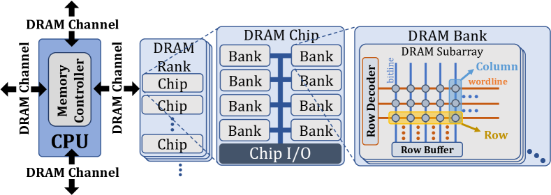
A DRAM chip consists of multiple DRAM banks, which share an internal bus that connects them to the chip’s I/O circuitry. Within a DRAM bank, DRAM cells are organized into multiple (e.g., 128) dense two-dimensional arrays of DRAM cells called subarrays [3, 41, 128] and corresponding peripheral circuitry for manipulating the data within the subarray. A row of cells (i.e., DRAM row) within a subarray share a wire (i.e., wordline), which is driven by a row decoder to open (i.e., select) the row of cells to be read or written. A column of cells (i.e., DRAM column) within a subarray share a wire (i.e., bitline), which is used to read and write to the cells with the help of a row buffer (consisting of sense amplifiers). This hierarchical layout of DRAM cells enables any data in the DRAM system to be accessed and updated using unique channel, rank, bank, row, and column addresses.
2.2 DRAM Operation
The memory controller interfaces with DRAM using a series of commands sent over the I/O bus. There are four major commands that are used to access DRAM: ACT, WR, RD, and PRE. DRAM command scheduling [143, 169, 170, 171, 172, 173, 174] is tightly regulated by a set of timing parameters, which guarantee that enough time passes after a certain command such that DRAM provides or retains data correctly. DRAM commands and timing parameters are defined by DRAM standards [8, 44, 44, 175] and they constitute part of the interface between the memory controller and the DRAM chip.
Figure 2.2, which we explain in the next several subsections, illustrates the relationship between the commands issued to perform a DRAM read, their governing timing parameters, and their effect on cell and bitline voltages. The memory controller enforces relevant timing parameters as it schedules each DRAM command. Aside from the DRAM access commands, the memory controller also periodically issues a refresh (REF) command to prevent data loss due to leakage of charge from the cell capacitors over time.
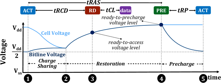
2.2.1 Activate (ACT)
The ACT command activates (opens) a DRAM row by transferring the data contained in the cell capacitors to the row buffer. ACT latency is governed by the tRCD timing parameter, which ensures that enough time has passed since the ACT is issued for the data to stabilize in the row buffer (such that it can be read by issuing a RD command).
ACT consists of two major steps: 1) capacitor-bitline charge sharing and 2) charge restoration. Charge sharing begins by enabling the wordline ( in Figure 2.2), which allows the cell capacitor to share charge with the bitline, and thus perturb the precharged bitline voltage. Once the cell and bitline voltages equalize due to charge sharing, charge restoration starts ( ). During charge restoration, the sense amplifiers are enabled to first detect the bitline voltage shift, and later restore the bitline to a full or depending on the direction of the shift. Once the bitline is restored to a ready-to-access voltage level ( ), the other DRAM commands (e.g., RD, WR) can be issued to the bank.
2.2.2 Read (RD)
After a row activation, the memory controller reads data from the open row by issuing a RD command. The RD command includes a column address, which indicates the portion of the open row to be read. When a DRAM chip receives a RD command, it first loads the requested portion of the open row into the global row buffer. After the data is in the global row buffer, the DRAM chip sends the data across the data bus to the memory controller. The RD command is governed by the timing parameter tCL, after which the data appears on the data bus.
2.2.3 Write (WR)
The WR command (not shown in Figure 2.2) modifies data in an open DRAM row. The operation of WR is analogous to ACT in that both commands require waiting enough time for the sense amplifiers to restore the data in the DRAM cells. Similar to how a sense amplifier restores a cell capacitor during the second step of ACT (i.e., charge restoration), in case of a WR, the sense amplifier restores the capacitor with the new data value that the WR command provides. The restoration latency for WR is governed by the tWR timing parameter. For both ACT and WR commands, the restoration latency originates from the sense amplifier driving a bitline to replenish the charge of the DRAM cell capacitor [3, 42, 11, 176].
2.2.4 Precharge (PRE)
PRE is used to close an open DRAM row and prepare the DRAM bank for activation of another row. The memory controller can follow an ACT with PRE to the same bank after at least the time interval specified by the tRAS timing parameter. tRAS ensures that enough time has passed to fully restore the DRAM cells of the activated row to a ready-to-precharge voltage ( in Figure 2.2). The latency of PRE is governed by the tRP timing parameter, which allows enough time to set the bitline voltage back to the reference voltage level (e.g., ). After tRP ( in Figure 2.2), the memory controller can issue an ACT to open a new row in the same bank.
2.2.5 Refresh (REF)
A DRAM cell cannot store its data permanently, as the cell capacitor leaks charge over time. The retention time of a DRAM cell is defined as the length of time for which the data can still be correctly read out of the cell after data is stored in the cell. To ensure data integrity, a DRAM cell must be periodically refreshed. To enable such periodic refresh of all DRAM cells, the memory controller periodically issues a refresh (REF) command (e.g., every or in chips implementing the DDR4 standard [8]) to ensure that every DRAM cell is refreshed once at a fixed refresh window (i.e., typically 32 or in chips implementing the DDR4 standard [8]) [177, 7, 65, 43, 175, 8, 118, 44]. A DRAM chip refreshes several (e.g., ) rows upon receiving a single REF command, which takes tRFC (e.g., ) to complete. Typically REF commands are required to refresh the entire DDR4 DRAM chip in a refresh window. The new DDR5 standard [44] similarly completes refreshing the entire DRAM chip with REF commands but requires or refresh window, i.e., a REF is issued every when operating at up to and when operating between -.
2.3 DRAM Performance Issues
In this section, we discuss the major performance issues of DRAM that we tackle in this dissertation.
2.3.1 DRAM Access Latency
In contrast to tremendous improvement in DRAM chip density, DRAM access latency has reduced only slightly [2, 11, 17, 39, 16, 178, 10, 179, 180, 12, 181, 9, 13]. Over the last two decades, DRAM density increased by more than two orders of magnitude, whereas tRCD and tRAS latencies decreased by only 0.81% and 1.33% per year between 2000 and 2015 [13].
Even though technology node scaling would normally reduce latencies in the DRAM circuit in conjunction with enabling higher DRAM capacity, DRAM vendors typically design their DRAM chips to trade the latency reduction for further improvements in DRAM capacity. For example, vendors amortize the large area cost of a sense amplifier by increasing the number of DRAM cells connected to the same sense amplifier, which increases the bitline length [17, 2]. Increasing the bitline length leads to higher resistance and parasitic capacitance on the connections between a DRAM cell and a sense amplifier. Consequently, a long bitline results in higher access latency than a short bitline.
To reduce the long DRAM latencies, many prior works propose various techniques that exploit temporal charge variation in DRAM cells [17, 182, 183, 136], exploit design-induced latency variation [126, 184, 159], use in-DRAM caching [39, 124, 3, 185, 186, 133], make static [2, 37, 9, 187] and dynamic [15, 179] capacity-latency tradeoff, and reduce timing parameters under certain operating conditions [10, 99, 11].
2.3.2 DRAM Refresh Overhead
Periodic DRAM refresh operations incur high system performance (and energy consumption) overheads. As the DRAM cell size decreases with process technology scaling, newer DRAM devices contain more DRAM cells than older DRAM devices [40]. As a result, while DRAM capacity increases, the performance and energy overheads of the refresh operations scale unfavorably [41, 42, 43]. In modern LPDDR4 [188] devices, the memory controller refreshes every DRAM cell every (when temperature is above , every ). Previous studies show that 1) refresh operations incur large performance overheads, as DRAM cells cannot be accessed when the cells are being refreshed [41, 43, 45, 46]; and 2) up to 50% of the total DRAM energy is consumed by the refresh operations [43, 41].
To mitigate DRAM refresh overhead, prior works propose various techniques that exploit retention time variation [43, 57, 50, 189, 162, 190, 45, 122, 49, 191], simultaneously activate multiple DRAM rows [192, 124, 179], parallelize refreshes with accesses [41, 113], optimize scheduling of refresh commands [51, 53, 54, 55, 46, 58, 59], and exploit data pattern variation [66, 67, 68, 69, 193].
2.4 DRAM Reliability Issues
In this section, we discuss the major reliability issues of DRAM that we tackle in this dissertation.
2.4.1 Charge Leakage and Data Retention
A DRAM cell stores a data value in the form of charge in its capacitor (e.g., a charged cell can represent 0 or 1 and vice versa). Since the capacitor naturally loses charge over time, the capacitor charge must be actively and periodically refreshed to prevent information loss due to a data retention failure [122, 177, 7, 65, 66, 69, 68, 43, 67, 49, 194, 11, 159, 178, 10, 99, 1, 163, 160, 162, 195, 73, 12, 126, 196, 197, 198, 199, 166, 200, 141]. As we explain in section 2.3.2, DRAM refresh incurs significant system performance and energy consumption overheads.
Although all DRAM cell in a DRAM chip are refreshed at a fixed refresh interval, the retention times of different cells can significantly vary [122, 43, 49, 69, 67, 68, 66, 65, 194, 11]. Many prior works [65, 49, 69, 67, 68, 66, 194, 11, 122, 159, 178, 10, 99, 1, 163, 160, 162, 195, 73, 12, 126, 196, 197, 198, 199, 166, 200, 141] perform detailed experimental studies to analyze data retention and reliability characteristics of real DRAM chips. Other prior works [201, 43, 156, 202, 191, 203] propose techniques to mitigate DRAM retention failures.
2.4.2 Violating Access and Refresh Timings
DRAM vendors specify timing parameters that a memory controller must satisfy when accessing and refreshing their DRAM chip in order to ensure reliable operation. However, deliberately violating DRAM timing parameters is useful for several cases. First, as we explain in section 2.3.1, violating DRAM timing parameters can improve DRAM latency and energy efficiency at the cost of increased bit error rate. Second, prior works show that deliberately violating DRAM timing parameters provides new functions like Physical Unclonable Functions (PUFs)[137, 204, 108, 109, 205], True Random Number Generators (TRNGs)[102, 139, 105, 206, 107, 207], and computation using DRAM [101, 129, 128, 106, 208]. Third, DRAM errors caused by violating DRAM timing parameters are useful for understanding various DRAM properties and behavior under different operating conditions [65, 49, 69, 67, 68, 66, 194, 11, 122, 159, 178, 10, 99, 1, 163, 160, 162, 195, 73, 12, 126, 196, 197, 198, 199, 166, 200, 141] and reverse-engineering DRAM circuit design [13, 141, 135, 209, 10, 103, 163, 184, 137, 165, 11, 210, 71].
2.4.3 Variable Retention Time (VRT)
Variable Retention Time (VRT) [211, 49, 63, 212, 213, 214, 215, 216, 217, 218, 66, 42, 65] is a phenomenon where certain DRAM cells switch between low and high retention time states in an unpredictable manner. When in low retention time state, a DRAM cell becomes more likely to experience a retention error. Therefore, VRT effects make accurately profiling the retention time of DRAM cells difficult. With DRAM technology scaling, VRT grows into an even more critical problem [219, 42, 220]. Despite the efforts to identify and mitigate VRT-related DRAM errors [49, 221, 122, 66, 67, 68, 69, 11, 102], VRT still remains as a key DRAM scaling challenge [42, 65].
2.4.4 Environmental Factors
Various environmental factors degrade the reliability of a DRAM chip. First, random external events such as particle strikes [222, 223, 224, 225, 199, 197, 226] may cause transient bit flips in DRAM. Second, prior experimental studies [65, 227, 228, 229, 230, 122, 66, 67, 68, 69, 231] show that increase in DRAM operation temperature significantly accelerates charge leakage, leading to lower DRAM cell retention times. Thus, high operating temperatures, especially temperatures above the range specified by DRAM vendors (e.g., [8, 44, 118, 177, 175]), can severely impact the reliability of a DRAM chip. Third, a DRAM chip may suffer from increased reliability issues when set to operate at reduced supply voltage. Chang et al. [99] analyzes the DRAM bit errors at reduces voltage levels and observes that such bit errors can be avoided by increasing DRAM access timing parameters. Fourth, prior studies [197, 232, 196] report that aging is an important factor affecting DRAM reliability and lifetime. Only after 10-18 months of being in use, DRAM chips exhibit increased error rates [197].
2.5 DRAM Security Issues
In this section, we discuss RowHammer and cold boot attacks, which are major security issues of DRAM. We tackle RowHammer in this dissertation, but our findings and techniques can potentially be useful for tackling cold boot attacks as well.
2.5.1 RowHammer
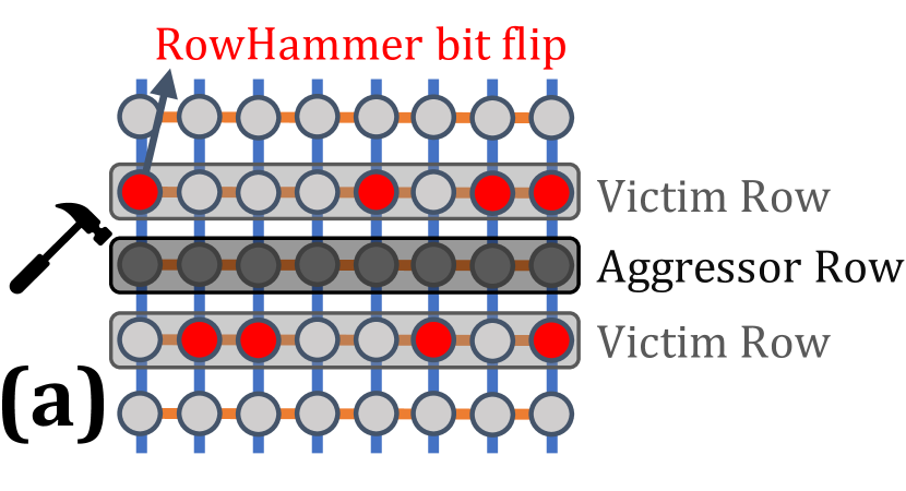
Modern DRAM chips suffer from disturbance errors that occur when a high number of activations (within a refresh window) to one DRAM row unintentionally affects the values of cells in nearby rows [73]. This phenomenon, popularly called RowHammer [73, 74, 72, 76], stems from electromagnetic interference between circuit elements. RowHammer becomes exacerbated as manufacturing process technology node size (and hence DRAM cell size) shrinks and circuit elements are placed closer together [70, 72]. As demonstrated in prior works [73, 70, 71, 75, 103, 134, 100, 119], the RowHammer effect is strongest between immediately physically-adjacent rows. RowHammer bit flips are most likely to appear in neighboring rows physically adjacent to a hammered row that is activated many times (e.g., in DDR3 [73], in DDR4 [70], and in LPDDR4 [70])111For DDR3 chips, [73] reports the minimum number of row activations on a single aggressor row (i.e., single-sided RowHammer) to cause a RowHammer bit flip. For DDR4 and LPDDR4 chips, [70] reports the minimum number of row activations to each of the two immediately-adjacent aggressor rows (i.e., double-sided RowHammer).. A hammered row is also called an aggressor row and a nearby row that is affected by the hammered row is called a victim row, regardless of whether or not the victim row actually experiences RowHammer bit flips.
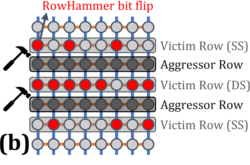
To most effectively exploit the RowHammer phenomenon, attackers typically perform ) single-sided RowHammer (i.e., repeatedly activate one aggressor row that is physically adjacent to the victim row, as we show in Fig. 2.3a) [73] or ) double-sided RowHammer (i.e., repeatedly activate in an alternating manner two aggressor rows that are both physically adjacent to the victim row, as we show in Fig. 2.3b) [233, 234]. Prior works have shown that double-sided RowHammer leads to more bit flips and does so more quickly than single-sided RowHammer [73, 70, 74, 233, 234, 71, 75, 103, 134, 100, 119].
Since the discovery of RowHammer, researchers have proposed many techniques that take advantage of the RowHammer vulnerability to compromise operating systems [233, 83, 235, 236, 77, 237, 238, 239, 240, 241, 242, 134, 243, 244], web browsers [245, 246, 100, 247, 248], cloud virtual machines [249, 250], remote servers [251, 252], and deep neural networks [253, 254]. To mitigate RowHammer, early solutions were immediate quick fixes such as increasing the DRAM refresh rate [80, 255, 256, 257] and relying on ECC to fix RowHammer bit flips [73, 233, 249, 235, 245], which were shown to be ineffective [77, 84, 73]. Other solutions include isolating sensitive data from DRAM rows that an attacker can hammer [81, 82, 83], keeping track of row activation counts and refreshing potential victim rows [84, 73, 85, 79, 86, 87, 88, 90, 91, 92, 93, 258, 94, 259, 95, 96], throttling row activations to prevent a row from being activated more than a certain threshold [78, 73, 89], and reducing wordline voltage [75].
To this date, DRAM vendors implement proprietary in-DRAM RowHammer solutions. Despite the claims of the DRAM vendors that their DRAM chips are “RowHammer-free” [115], prior works [100, 103, 119] demonstrate that certain carefully-crafted access patterns can be used to bypass these in-DRAM protection mechanisms. In chapter 4, we further discuss the operation and security properties of RowHammer protection mechanisms implemented in current DRAM devices.
2.5.2 Cold Boot Attacks
When a DRAM chip is powered off, the DRAM cells in the chip are expected to lose their values as cells can no longer be refreshed. However, the majority of DRAM cells are capable of correctly retaining their data for much longer than the typical 64 or refresh period [65, 122, 69, 68, 67, 66, 11, 231, 194, 49]. Cooling the DRAM chip further extends the retention capability of DRAM cells because their charge leakage rates greatly decrease as the operating temperature reduces [65, 227, 228, 229, 230, 122, 66, 67, 68, 69, 231]. Halderman et al. [231] show that a DRAM chip can correctly retain 99.9% of its data for minutes when cooled down to using a compressed air can. The fact that a DRAM chip retains the majority of its data after a power loss poses a critical security problem. An attacker can retrieve sensitive information (e.g., encryption keys) from a DRAM chip by plugging in the chip to a machine that the attacker owns. To mitigate DRAM cold boot attacks, prior works propose techniques that obfuscate data written to DRAM [260, 261, 262, 263], store encryption keys only in CPU registers [264, 265], use full memory encryption [266, 267], and erase DRAM content [106, 268].
?chaptername? 3 SoftMC: A Flexible and Practical Open-Source Infrastructure
for Enabling Experimental DRAM Studies
DRAM process technology node scaling leads to key challenges that critically impact DRAM reliability and performance. To accurately understand the DRAM cell behavior in terms of reliability and latency, it is critical to characterize and analyze real DRAM chips. In this chapter, we design, prototype, and demonstrate the basic capabilities of a flexible and easy-to-use experimental DRAM characterization infrastructure, called SoftMC (Soft Memory Controller). SoftMC is an open-source FPGA-based DRAM characterization infrastructure, consisting of a programmable memory controller that can control and test memory modules designed for the commonly-used DDR (Double Data Rate) interface. SoftMC provides a simple and intuitive high-level programming interface that completely hides the low-level details of the FPGA from users. Users implement their test routines or mechanisms in a high-level language that automatically gets translated into the low-level SoftMC memory controller operations in the FPGA.
SoftMC offers a wide range of use cases, such as characterizing the effects of variation within a DRAM chip and across DRAM chips, verifying the correctness of new DRAM mechanisms on actual hardware, and experimentally discovering the reliability, retention, and timing characteristics of an unknown or newly-designed DRAM chip (or finding the best specifications for a known DRAM chip). We demonstrate the potential and ease of use of SoftMC by implementing two use cases. First, we demonstrate the ease of use of SoftMC’s high-level interface by implementing a simple experiment to characterize the retention time behavior of cells in modern DRAM chips. Our test results match the prior experimental studies that characterize DRAM retention time in modern DRAM chips [43, 65, 66, 49], providing a validation of our infrastructure. Second, we demonstrate the flexibility and capability of SoftMC by validating two recently-proposed DRAM latency reduction mechanisms [17, 182]. These mechanisms exploit the idea that highly-charged DRAM cells can be accessed with low latency. Our SoftMC-based experimental analysis of 24 real DRAM chips from three major DRAM vendors demonstrates that the expected latency reduction effect of these mechanisms is not observable in existing DRAM chips. This experiment demonstrates (i) the importance of experimentally characterizing real DRAM chips to understand the behavior of DRAM cells, and designing mechanisms that are based on this experimental understanding; and (ii) the effectiveness of SoftMC in testing (validating or refuting) new ideas on existing memory modules.
We also discuss several other use cases of SoftMC, including the ability to characterize emerging non-volatile memory modules that obey the DDR standard. We hope that SoftMC inspires other new studies, ideas, and methodologies in memory system design. In fact, since the release of SoftMC to the public as part of this research, many works [29, 10, 99, 100, 71, 101, 70, 102, 103, 69, 104, 75, 105, 106, 107, 108, 109, 110, 111, 112, 113, 114] used different versions of SoftMC in various DRAM characterization studies. SoftMC is openly and freely available at [98].
3.1 Motivation and Goal
At smaller technology nodes, it is becoming increasingly difficult to store and retain enough charge in a DRAM cell, causing various reliability and performance issues [65, 61, 5, 62, 63, 64, 43, 66, 67, 68, 69, 6, 70, 71, 72, 73, 74, 75, 41, 49, 47, 57, 56, 59, 60]. Ensuring reliable operation of the DRAM cells is a key challenge in future technology nodes [5, 61, 269, 270, 43, 42, 65, 62, 63, 64, 66, 67, 68, 69, 6, 70, 71, 72, 73, 74, 75].
The fundamental problem of retaining data with less charge in smaller cells directly impacts the reliability and performance of DRAM cells. First, smaller cells placed in close proximity make cells more susceptible to various types of interference. This potentially disrupts DRAM operation by flipping bits in DRAM, resulting in major reliability issues [73, 271, 62, 197, 272, 196, 5, 61, 269, 270, 43, 42, 65, 63, 64, 66, 67, 68, 69, 6, 70, 71, 72, 74, 75], which can lead to system failure [197, 196, 77, 74, 134] or security breaches [73, 233, 234, 236, 235, 250, 249, 83, 77, 237, 238, 239, 240, 241, 242, 134, 243, 244, 245, 246, 100, 247, 248, 251, 252, 253, 254]. Second, it takes longer time to access a cell with less charge [17, 11, 182, 126, 10, 99, 183], and write latency increases as the access transistor size reduces [42, 11, 183]. Thus, smaller cells directly impact DRAM latency, as DRAM access latency is determined by the worst-case (i.e., slowest) cell in any chip [159, 11, 122, 126]. DRAM access latency has not improved with technology scaling in the past decade [2, 16, 5, 11, 17, 39, 178, 10, 179, 180, 12, 181, 9, 13], and, in fact, some latencies are expected to increase [42], making memory latency an increasingly critical system performance bottleneck.
As such, there is a significant need for new mechanisms that improve the reliability and performance of DRAM-based main memory systems. In order to design, evaluate, and validate many such mechanisms, it is important to accurately characterize, analyze, and understand DRAM (cell) behavior in terms of reliability and latency. For such an understanding to be accurate, it is critical that the characterization and analysis be based on the experimental studies of real DRAM chips, since a large number of factors (e.g., various types of cell-to-cell interference [271, 62, 73, 70, 71], inter- and intra-die process variation [10, 12, 273, 159, 11, 126], random effects [65, 63, 274, 275, 49], operating conditions [65, 276, 99, 75, 71], internal organization [65, 277, 68, 126], stored data patterns [67, 68, 65, 69, 66, 49, 70, 71]) concurrently impact the reliability and latency of cells. Many of these phenomena and their interactions cannot be properly modeled (e.g., in simulation or using analytical methods) without rigorous experimental characterization and analysis of real DRAM chips. The need for such experimental characterization and analysis, with the goal of building the understanding necessary to improve the reliability and performance of future DRAM-based main memories at various levels (both software and hardware), motivates the need for a publicly-available DRAM testing infrastructure that can enable system users and designers to characterize real DRAM chips.
A publicly-available DRAM testing infrastructure that can characterize real DRAM chips enables new mechanisms to improve DRAM reliability and latency. In this work, we argue that such a testing infrastructure should have two key features to ensure widespread adoption among architects and designers: (i) flexibility and (ii) ease of use.
Flexibility. As discussed in section 2.2, a DRAM module is accessed by issuing specific commands (e.g., ACT, PRE) in a particular sequence with a strict delay between the commands (specified by the timing parameters, e.g., tRP, tRAS). A DRAM testing infrastructure should implement all low-level DRAM operations (i.e., DDR commands) with tunable timing parameters without any restriction on the ordering of DRAM commands. Such a design enables flexibility at two levels. First, it enables comprehensive testing of any DRAM operation with the ability to customize the length of each timing constraint. For example, we can implement a retention test with different refresh intervals to characterize the distribution of retention time in modern DRAM chips. Such a characterization can enable new mechanisms to reduce the number of refresh operations in DRAM, leading to performance and power efficiency improvements. Second, it enables testing of DRAM chips with high-level test programs, which can consist of any combination of DRAM operations and timings. Such flexibility is extremely powerful to test the impact of existing or new DRAM mechanisms in real DRAM chips.
Ease of Use. A DRAM testing infrastructure should provide a simple and intuitive programming interface that minimizes programming effort and time. An interface that hides the details of the underlying implementation is accessible to a wide range of users. With such a high-level abstraction, even users that lack hardware design experience should be able to develop DRAM tests.
In this work, we propose and prototype a publicly-available, open-source DRAM testing infrastructure that can enable system users and designers to easily characterize real DRAM chips. Our experimental DRAM testing infrastructure, called SoftMC (Soft Memory Controller), can test DDR-based memory modules with a flexible and easy-to-use interface. In the next section, we discuss the shortcomings of existing tools and platforms that can be used to test DRAM chips, and explain how SoftMC is designed to avoid these shortcomings.
3.2 Related Work
No prior DRAM testing infrastructure provides both flexibility and ease of use properties, which are critical for enabling widespread adoption of the infrastructure. Three different kinds of tools/infrastructure are available today for characterizing DRAM behavior. As we will describe, each kind of tool has some shortcomings. The goal of SoftMC is to eliminate all of these shortcomings.
Commercial Testing Infrastructures. A large number of commercial DRAM testing platforms (e.g., [278, 279, 280, 281]) are available in the market. Such platforms are optimized for throughput (i.e., to test as many DRAM chips as possible in a given time period), and generally apply a fixed test pattern to the units under test. Thus, since they lack support for flexibility in defining the test routine, these infrastructures are not suitable for detailed DRAM characterization where the goal is to investigate new issues and new ideas. Furthermore, such testing equipment is usually quite expensive, which makes these infrastructures an impractical option for research in academia. Industry may also have internal DRAM development and testing tools, but, to our knowledge, these are proprietary and are unlikely to be made openly available.
We aim for SoftMC to be a low-cost (i.e., free) and flexible open-source alternative to commercial testing equipment that can enable new research directions and mechanisms. For example, prior work [282] recently proposed a random command pattern generator to validate DRAM chips against uncommon yet supported (according to JEDEC specifications) DDR command patterns. Using the test patterns on commercial test equipment, this work demonstrates that specific sequences of commands introduce failures in current DRAM chips. SoftMC flexibly supports the ability to issue an arbitrary command sequence, and therefore can be used as a low-cost method for validating DRAM chips against problems that arise due to command ordering.
FPGA-Based Testing Infrastructures. Several prior works proposed FPGA-based DRAM testing infrastructures [283, 228, 284]. Unfortunately, all of them lack flexibility and/or a simple user interface, and none are open-source. The FPGA-based infrastructure proposed by Huang et al. [283] provides a high-level interface for developing DRAM tests, but the interface is limited to defining only data patterns and march algorithms for the tests. Hou et al. [228] propose an FPGA-based test platform whose capability is limited to analyzing only the data retention time of the DRAM cells. Another work [284] develops a custom memory testing board with an FPGA chip, specifically designed to test memories at a very high data rate. However, it requires low-level knowledge to develop FPGA programs, and even then offers only limited flexibility in defining a test routine. On the other hand, SoftMC aims to provide full control over all DRAM commands using a high-level software interface, and it is open-source.
PARDIS [285] is a reconfigurable logic (e.g., FPGA) based programmable memory controller meant to be implemented inside microprocessor chips. PARDIS is capable of optimizing memory scheduling algorithms, refresh operations, etc. at run-time based on application characteristics, and can improve system performance and efficiency. However, it does not provide programmability for DRAM commands and timing parameters, and therefore cannot be used for detailed DRAM characterization.
Built-In Self Test (BIST). A BIST mechanism (e.g, [286, 287, 288, 289, 290]) is implemented inside the DRAM chip to enable fixed test patterns and algorithms. Using such an approach, DRAM tests can be performed faster than with other testing platforms. However, BIST has two major flexibility issues, since the testing logic is hard-coded into the hardware: (i) BIST offers only a limited number of tests that are fixed at hardware design time. (ii) A limited set of DRAM chips, which come with BIST support, can be tested. In contrast, SoftMC allows for the implementation of a wide range of DRAM test routines and supports any off-the-shelf DRAM chip that is compatible with the DDR interface.
We conclude that prior work lacks either the flexibility or the ease-of-use properties that are critical for performing detailed DRAM characterization. To fill the gap left by current infrastructures, we introduce an open-source DRAM testing infrastructure, SoftMC, that fulfills these two properties.
3.3 SoftMC Design
SoftMC is an FPGA-based open-source programmable memory controller that provides a high-level software interface, which the users can use to initiate any DRAM operation from a host machine. The FPGA component of SoftMC collects the DRAM operation requests incoming from the host machine and executes them on real DRAM chips that are attached to the FPGA board. In this section, we explain in detail the major components of our infrastructure.
3.3.1 High-Level Design
Figure 3.1 shows our SoftMC infrastructure. It comprises three major components:
-
In the host machine, the SoftMC API provides a high-level software interface (in C++) for users to communicate with the SoftMC hardware. The API provides user-level functions to 1) send SoftMC instructions from the host machine to the hardware and 2) receive data, which the hardware reads from the DRAM, back to the host machine. An instruction encodes and specifies an operation that the hardware is capable of performing (see section 3.3.4). It is used to communicate the user-level function to the SoftMC hardware such that the hardware can execute the necessary operations to satisfy the user-level function. The SoftMC API provides several functions (See section 3.3.3) that users can call to easily generate an instruction to perform any of the operations supported by the SoftMC infrastructure. For example, the API contains a genACT() function, which users call to generate an instruction to activate a row in DRAM.
-
The driver is responsible for transferring instructions and data between the host machine and the FPGA across a PCIe bus. To implement the driver, we use RIFFA [291]. SoftMC execution is not affected by the long transfer latency of the PCIe interface, as our design sends all of the instructions over the PCIe bus to the FPGA before the test routine begins, and buffers the commands within the FPGA. Therefore, SoftMC guarantees that PCIe-related delays do not affect the precise user-defined timings between each instruction.
-
Within the FPGA, the core SoftMC hardware queues the instructions, and executes them in an appropriate hardware component. For example, if the hardware receives an instruction that indicates a DRAM command, it sends DDR-compatible signals to the DRAM to issue the command.

3.3.2 DRAM Command Interface
DRAM commands are transmitted from the memory controller to the DRAM module across a memory bus. On the memory bus, each command is encoded using five output signals (CKE, CS, RAS, CAS, and WE). Enabling/disabling these signals corresponds to specific commands (as specified by the DDR standard). First, the CKE signal (clock enable) determines whether the DRAM is in “standby mode” (ready to be accessed) or “power-down mode”. Second, the CS (chip selection) signal specifies the rank that should receive the issued command. Third, the RAS (row address strobe)/CAS (column address strobe) signal is used to generate commands related to DRAM row/column operations. Fourth, the WE signal (write enable) in combination with RAS and CAS, generates the specific row/column command. For example, enabling CAS and WE together generates a WR command, while enabling only CAS indicates a RD command.
3.3.3 SoftMC API
SoftMC offers users complete control over the DDR-based DRAM memory modules by providing an API (Application Programming Interface) in a high-level programming language (C++). This API consists of several C++ functions that generate instructions for the SoftMC hardware, which resides in the FPGA. These instructions provide support for (i) all possible DDR DRAM commands; and (ii) managing the SoftMC hardware, e.g., inserting a delay between commands, configuring the auto-refresh mechanism (see section 3.3.5). Using the SoftMC API, any sequence of DRAM commands can be easily and flexibly implemented in SoftMC with little effort and time from the programmer.
When users would like to issue a sequence of commands to the DRAM, they only need to make SoftMC API function calls. Users can easily generate instructions by calling the API functions. Users can insert the generated instructions to an InstructionSequence, which is a data structure that the SoftMC API provides to keep the instructions in order and easily send them to the SoftMC hardware via the driver. There are three types of API functions: (i) command functions, which provide the user the ability to specify DDR-compatible DRAM commands (e.g., ACT, PRE); (ii) the wait function, which provide the user the ability to specify a time interval between two commands (thereby allowing the user to determine the latencies of each timing parameter); and (iii) aux functions, which provide the user with control over various auxiliary operations. Programming the memory controller using such high-level C++ function calls enables users who are inexperienced in hardware design to easily develop sophisticated memory controllers.
Command Functions. For every DDR command, we provide a command function that generates an instruction, which instructs the SoftMC hardware to execute the command. For example, genACT(b, r) function generates an instruction that informs the SoftMC controller to issue an ACT to DRAM row r in bank b. Program LABEL:softmc_code:softmc_write shows a short example program that writes to a single cache line (i.e., DRAM column) in a closed row. In Program LABEL:softmc_code:softmc_write, there are three command functions: genACT(), genWR(), and genPRE(), in lines 2, 4, and 6, which generate SoftMC hardware instructions that inform the SoftMC hardware to issue ACT, WR, and PRE commands to the DRAM.
Wait Function. We provide a single function, genWAIT(t), which generates an instruction to inform the SoftMC hardware to wait t DRAM cycles before executing the next instruction. With this one function, the user can implement any timing constraint. For example, in Program LABEL:softmc_code:softmc_write, the controller should wait for tRCD after the ACT before issuing a WR to the DRAM. We simply add a call to genWAIT() on Line 3 to insert the tRCD delay. Users can easily provide any value that they want to test for the time interval (e.g., a reduced tRCD, to see if errors occur when the timing parameter is reduced).
Aux Functions. There are a number of auxiliary functions that allow the user to configure the SoftMC hardware. One such function, genBUSDIR(dir), allows the user to switch (i.e., turn around) the DRAM bus direction. To reduce the number of IO pins, the DDR interface uses a bi-directional data bus between DRAM and the controller. The bus must be set up to move data from DRAM to the controller before issuing a RD, and from the controller to DRAM before issuing a WR. After genBUSDIR() is called, the user should follow it with a genWAIT() function, to ensure that the bus is given enough time to complete the turn around. The time interval for this wait corresponds to the tWTR and tRTW timing parameters in the DDR interface.
We provide an auxiliary function to control auto-refresh behavior. The SoftMC hardware includes logic to automatically refresh the DRAM cells after a given time interval (tREFI) has passed. Auto-refresh operations are not added to the code by the user, and are instead handled directly within our hardware. In order to adjust the interval at which refresh is performed, the user can invoke the genREF_CONFIG() function. To disable the auto-refresh mechanism, the user needs to set the refresh interval to 0 by calling that function. The user can invoke the same function to adjust the number of cycles that specify the refresh latency (tRFC). We describe the auto-refresh functionality of the SoftMC hardware in more detail in section 3.3.5.
Finally, we provide a function, genEND(), which generates an END instruction to inform the SoftMC hardware that the end of the instruction sequence has been reached, and that the SoftMC hardware can start executing the sequence. Note that the programmer should call iseq.execute(fpga) to send the instruction sequence to the driver, which in turn sends the sequence to the SoftMC hardware. Program LABEL:softmc_code:softmc_write shows an example of this in Lines 8–9.
3.3.4 Instruction Types and Encoding
Figure 3.2 shows the encodings for the key SoftMC instruction types.111We refer the reader to the source-code and manual of SoftMC for the encoding of all instruction types [98]. All SoftMC instructions are 32 bits wide, where the most-significant 4 bits indicate the type of the instruction.
| InstrType | ||||
| DDR (4) | unused (3) | CKE, CS (2), RAS, CAS, WE (6) | Bank (3) | Addr (16) |
| WAIT (4) | cycles (28) | |||
| BUSDIR (4) | unused (27) | dir (1) | ||
| END (4) | unused (28) | |||
DDR Instruction Type. Recall from section 3.3.2 that the DDR commands are encoded using several fields (e.g., RAS, CAS, WE) that correspond to the signals of the DDR interface, which sits between the memory controller and the DRAM. The SoftMC instructions generated by our API functions encode these same fields, as shown in the instruction encoding for the DDR type instructions in Figure 3.2. Thus, DDR type instructions can represent any DDR command from the DDR3 specification [7]. For example, the user needs to set CKE = 1, CS = 0, RAS = 0, CAS = 1, and WE = 1 to create an ACT command to open the row in the bank specified by Address and Bank, respectively. Other DDR commands can easily be represented by setting the appropriate instruction fields according to the DDR3 specification.
Other Instruction Types. Other instructions carry information to the FPGA using the bottom 28 bits of their encoding. For example, the WAIT instruction uses these bits to encode the wait latency, i.e., wait cycles. The BUSDIR instruction uses the least significant bit of the bottom 28 bits to encode the new direction of the data bus. The END instruction requires no additional parameters, using only the InstrType field.
3.3.5 Hardware Architecture
The driver sends the SoftMC instructions across the PCIe bus to the FPGA, where the SoftMC hardware resides. Figure 3.3 shows the five components that make up the SoftMC hardware: (i) an instruction receiver, which accumulates the instructions sent over the PCIe bus; (ii) an instruction dispatcher, which decodes each instruction into DRAM control signals and address bits, and then sends the decoded bits to the DRAM module through the memory bus; (iii) a read capture module, which receives data read from the DRAM and sends it to the host machine over PCIe; (iv) an auto-refresh controller; and (v) a calibration controller, responsible for ensuring data integrity on the memory bus. SoftMC also includes two interfaces: a PCIe bus controller and a DDR PHY. Next, we describe each of these components in detail.
Instruction Receiver. When the driver sends SoftMC instructions across the PCIe bus, the instruction receiver buffers them in an instruction queue until the END instruction is received. When the END instruction arrives, the instruction receiver notifies the instruction dispatcher that it can start fetching instructions from the instruction queue. Execution ends when the instruction queue is fully drained.
Instruction Dispatcher. The instruction dispatcher fetches an instruction, decodes it, and executes the operation that the instruction indicates, at the corresponding component. For example, if the type of the instruction is DDR, the dispatcher decodes the control signals and address bits from the instruction, and then sends them to the DRAM using the DDR PHY. Since the FPGAs operate at a lower frequency than the memory bus, the dispatcher supports fetching and issuing of multiple DDR commands per cycle. As another example, if the instruction type is WAIT, it is not sent to the DRAM, but is instead used to count down the number of cycles before the instruction dispatcher can issue the next instruction to the DRAM. Other instruction types (e.g., BUSDIR, END) are handled in a similar manner.
Read Capture Module. After a RD command is sent to the DRAM module, the read capture module receives the data emitted by the DRAM from the DDR PHY, and sends it to the host machine via the PCIe controller. The read capture module is responsible for ensuring data alignment and ordering, in case the DDR PHY operates on a different clock domain or reorders the data output.
Auto-Refresh Controller. The auto-refresh controller includes two registers, which store the refresh interval (tREFI) and refresh latency (tRFC) values (See section 2.2). It issues periodic refresh operations to DRAM, based on the values stored in the registers. If the instruction dispatcher is in the middle of executing an instruction sequence that was received from the host machine, at the time a refresh is scheduled to start, the auto-refresh controller delays the refresh operation until the dispatcher finishes the execution of the instruction sequence. Note that a small delay does not pose any problems, as the DDR standard allows for a small amount of flexibility for scheduling refresh operations [41, 7, 45]. However, if the instruction sequence is too long, and delays the refresh operation beyond a critical interval (i.e., more than 8X the tREFI), it is the user’s responsibility to redesign the test routine and split up the long instruction sequence into smaller sequences.
Calibration Module. This module ensures the data integrity of the memory bus. It periodically issues a command to perform short ZQ calibration, which is an operation specified by the DDR standard to calibrate the output driver and on-die termination circuits [177, 292]. SoftMC provides hardware support for automatic calibration, in order to ease programmer effort.
PCIe Controller and DDR PHY. The PCIe controller acts as an interface between the host machine and the rest of the SoftMC hardware. The DDR PHY sits between the SoftMC hardware and the DRAM module, and is responsible for initialization and clock synchronization between the FPGA and the DRAM module.
3.3.6 SoftMC Prototype
We describe the key implementation details of our first prototype of SoftMC.
FPGA Board. The current SoftMC prototype targets a Xilinx ML605 FPGA board [293]. It consists of (i) a Virtex-6 FPGA chip, which we use to implement our SoftMC design; and (ii) a SO-DIMM slot, where we plug in the real DRAM modules to be tested.
PCIe Interface. The PCIe controller uses (i) the Xilinx PCIe Endpoint IP Core [294], which implements low-level operations related to the physical layer of the PCIe bus; and (ii) the RIFFA IP Core [291], which provides high-level protocol functions for data communication. The communication between the host machine and the FPGA board is established through a PCIe 2.0 link.
DDR PHY. SoftMC uses the Xilinx DDR PHY IP Core [295] to communicate with the DRAM module. This PHY implements the low-level operations to transfer data over the memory channel to/from the DRAM module. The PHY transmits two DDR commands each memory controller cycle. As a result, our SoftMC implementation fetches and dispatches two instructions from the instruction queue every cycle.
Performance. To evaluate the performance of our prototype, we time the execution of a test routine that performs operations on a particular region of the DRAM and then reads data back from this region, repeating the test on different DRAM regions until the entire DRAM module has been tested. We model the expected overall execution time of the test as:
| (3.1) |
where S (Send), E (Execute), and R (Receive) are the host-to-FPGA PCIe latency, execution time of the command sequence in the FPGA, and FPGA-to-host PCIe latency, respectively, that is required for each DRAM region. For our prototype, we measure S and R to both be on average (with variation). E varies based on the length of the command sequence. For the sequence given in Program LABEL:softmc_code:write_row, which we use in our first use case (section 3.4.1), we calculate E as using typical DDR3 timing parameters. Since that command sequence tests only a single 8KB row, the Region Size is 8KB. For an experiment testing a full 4GB memory module completely, we find that our prototype runs Program LABEL:softmc_code:write_row on the entire module in approximately 31.5 seconds. An at-speed DRAM controller, which, at best, has S and R equal to zero, would run the same test in approximately 11.5 seconds, i.e., only 2.7x faster. As E increases, the performance of our SoftMC prototype gets closer to the performance of an at-speed DRAM controller. We conclude that our SoftMC prototype is fast enough to run test routines that cover an entire memory module.
3.4 Example Use Cases
Using our SoftMC prototype, we perform two case studies on randomly-selected real DRAM chips from three manufacturers. First, we discuss how a simple retention test can be implemented using SoftMC, and present the experimental results of that test (section 3.4.1). Second, we demonstrate how SoftMC can be leveraged to test the expected effect of two recently-proposed mechanisms that aim to reduce DRAM access latency (section 3.4.2). Both use cases demonstrate the flexibility and ease of use of SoftMC.
3.4.1 Retention Time Distribution Study
This test aims to characterize data retention time in different DRAM modules. The retention time of a cell can be determined by testing the cell with different refresh intervals. The cell fails at a refresh interval that is greater than its retention time. In this test, we gradually increase the refresh interval from the default and count the number of bytes that have an incorrect value at each refresh interval.
3.4.1.1 Test Methodology
We perform a simple test to measure the retention time of the cells in a DRAM chip. Our test consists of three steps: (i) We write a reference data pattern (e.g. all zeros, or all ones) to an entire row. (ii) We wait for the specified refresh interval, so that the row is idle for that time and all cells gradually leak charge. (iii) We read data back from the same row and compare it against the reference pattern that we wrote in the first step. Any mismatch indicates that the cell could not hold its data for that duration, which resulted in a bit flip. We count the number of bytes that have bit flips for each test.
We repeat this procedure for all rows in the DRAM module. The read and write operations in the test are issued with the standard timing parameters, to make sure that the only timing delay that affects the cells is the refresh interval.
3.4.1.2 Implementation with SoftMC.
Writing Data to DRAM. In Program LABEL:softmc_code:write_row, we present the implementation of the first part of our retention time test, where we write data to a row, using the SoftMC API. First, to activate the row, we insert the instruction generated by the genACT() function to an instance of the InstructionSequence (Lines 1-2). This function is followed by a genWAIT() function (Line 3) that ensures that the activation completes with the standard timing parameter tRCD. Second, we issue write instructions to write the data pattern in each column of the row. This is implemented in a loop, where, in each iteration, we call genWR() (Line 5), followed by a call to genWAIT() function (Line 6) that ensures proper delay between two WR operations. After writing to all columns of the row, we insert another delay (Line 8) to account for the write recovery time (section 2.2). Third, once we have written to all columns, we close the row by precharging it. This is done by the genPRE() function (Line 9), followed by a genWAIT() function with standard tRP timing. Finally, we call the genEND() function to indicate the end of the instruction sequence, and send the test program to the FPGA by calling the execute() function.
Employing a Specific Refresh Interval. Using SoftMC, we can implement the target refresh interval in two ways. We can use the auto-refresh support provided by the SoftMC hardware, by setting the tREFI parameter to our target value, and letting the FPGA take care of the refresh operations. Alternatively, we can disable auto-refresh, and manually control the refresh operations from the software. In this case, the user is responsible for issuing refresh operations at the right time. In this retention test, we disable auto-refresh and use a software clock to determine when we should read back data from the row (i.e., refresh the row).
Reading Data from DRAM. Reading data back from the DRAM requires steps similar to DRAM writes (presented in Program LABEL:softmc_code:write_row). The only difference is that, instead of issuing a WR command, we need to issue a RD command and enforce read-related timing parameters. In the SoftMC API, this is done by calling the genRD() function in place of the genWR() function, and specifying the appropriate read-related timing parameters. After the read operation is done, the FPGA sends back the data read from the DRAM module, and the user can access that data using the fpga_recv() function provided by the driver.
Based on the intuitive code implementation of the retention test, we conclude that it requires minimal effort to write test programs using the SoftMC API. Our full test is provided in our open-source release [98].
3.4.1.3 Results
We perform the retention time test at room temperature, using 24 chips from three major manufacturers. We vary the refresh interval from to exponentially. Figure 3.4 shows the results for the test, where the x-axis shows the refresh interval in milliseconds, and the y-axis shows the number of erroneous bytes found in each interval. We make two major observations.
(i) We do not observe any retention failures until we test with a refresh interval of . This shows that there is a large safety margin for the refresh interval in modern DRAM chips, which is conservatively set to by the DDR standard.222DRAM manufacturers perform retention tests that are similar to ours (but with proprietary in-house infrastructures that are not disclosed). Their results are similar to ours [65, 11, 66, 10], showing significant margin for the refresh interval. This margin is added to ensure reliable DRAM operation for the worst-case operating conditions (i.e., worst case temperature) and for worst-case cells, as has been shown by prior works [11, 65, 66, 10].
(ii) We observe that the number of failures increases drastically with the increase in refresh interval.
Prior experimental studies on retention time of DRAM cells have reported similar observations as ours [66, 65, 11, 228, 227]. We conclude that SoftMC can easily reproduce prior known DRAM experimental results, validating the correctness of our testing infrastructure and showing its flexibility and ease of use.
3.4.2 Evaluating the Expected Effect of Two Recently-Proposed Mechanisms in Existing DRAM Chips
Two recently-proposed mechanisms, ChargeCache [17] and NUAT [182], provide low-latency access to highly-charged DRAM cells. They both are based on the key idea that a highly-charged cell can be accessed faster than a cell with less charge [11]. ChargeCache observes that cells belonging to recently-accessed DRAM rows are in a highly-charged state and that such rows are likely to be accessed again in the near future. ChargeCache exploits the highly-charged state of these recently-accessed rows to lower the latency for later accesses to them. NUAT observes that recently-refreshed cells are in highly-charged state, and thus it lowers the latency for accesses to recently-refreshed rows. Prior to issuing an ACT command to DRAM, both ChargeCache and NUAT determine whether the target row is in a highly-charged state. If so, the memory controller uses reduced tRCD and tRAS timing parameters to perform the access.
In this section, we evaluate whether or not the expected latency reduction effect of these two works is observable in existing DRAM modules, using SoftMC. We first describe our methodology for evaluating the improvement in the tRCD and tRAS parameters. We then show the results we obtain using SoftMC, and discuss our observations.
3.4.2.1 Evaluating DRAM Latency with SoftMC.
Methodology. In our experiments, we use 24 DDR3 chips (i.e., three SO-DIMMs) from three major vendors. To stress DRAM reliability and maximize the amount of cell charge leakage, we raise the test temperature to 80∘C (significantly higher than the common-case operating range of 35-55∘C [11]) by enclosing our FPGA infrastructure in a temperature-controlled heat chamber (see Figure 3.1). For all experiments, the temperature within the heat chamber was maintained within 0.5∘C of the target 80∘C temperature.
To study the impact of charge variation in cells on access latency in existing DRAM chips, which is dominated by the tRCD and tRAS timing parameters [2, 11, 10] (see section 2.2), we perform experiments to test the headroom for reducing these parameters. In our experiments, we vary one of the two timing parameters, and test whether the original data can be read back correctly with the reduced timing. If the data that is read out contains errors, this indicates that the timing parameter cannot be reduced to the tested value without inducing errors in the data. We perform the tests using a variety of data patterns (e.g., 0x00, 0xFF, 0xAA, 0x55) because 1) different DRAM cells store information (i.e., 0 or 1) in different states (i.e., charged or empty) [65] and 2) we would like to stress DRAM reliability by increasing the interference between adjacent bitlines [68, 65, 67]. We also perform tests using different refresh intervals, to study whether the variation in charge leakage increases significantly if the time between refreshes increases.
tRCD Test. We measure how highly-charged cells affect the tRCD timing parameter, by using a custom tRCD value to read data from a row to which we previously wrote a reference data pattern. We adjust the time between writing a reference data pattern and performing the read, to vary the amount of charge stored within the cells of a row. In Figure 3.5(a), we show the command sequence that we use to test whether recently-refreshed DRAM cells can be accessed with a lower tRCD, compared to cells that are close to the end of the refresh interval. We perform the write and read operations to each DRAM row one column at a time, to ensure that each read incurs the tRCD latency. First ( in Figure 3.5(a)), we perform a reference write to the DRAM column under test by issuing ACT, WR, and PRE successively with the default DRAM timing parameters. Next ( ), we wait for the duration of a time interval (T1), which is the refresh interval in practice, to vary the charge contained in the cells. When we wait longer, we expect the target cells to have less charge at the end of the interval. We cover a wide range of wait intervals, evaluating values between 1 and . Finally ( ), we read the data from the column that we previously wrote to and compare it with the reference pattern. We perform the read with the custom tRCD value for that specific test. We evaluate tRCD values ranging from 3 to 6 (default) cycles. Since a tRCD of 3 cycles produced errors in every run, we did not perform any experiments with a lower tRCD.
We process multiple rows in an interleaved manner (i.e., we write to multiple rows, wait, and then verify their data one after another) in order to further stress the reliability of DRAM [11]. We repeat this process for all DRAM rows to evaluate the entire memory module.
tRAS Test. We measure the effect of accessing highly-charged rows on the tRAS timing parameter by issuing the ACT and PRE commands, with a custom tRAS value, to a row. We check if that row still contains the same data that it held before the ACT-PRE command pair was issued. Figure 3.5(b) illustrates the methodology for testing the effect of the refresh interval on tRAS. First ( ), we write the reference data pattern to the selected DRAM row with the default timing parameters. Different from the tRCD test, we write to every column in the open row (before switching to another row) to save cycles by eliminating a significant amount of ACT and PRE commands, thereby reducing the testing time. Next ( ), we wait for the duration of time interval T2, during which the DRAM cells lose a certain amount of charge. To refresh the cells ( ), we issue an ACT-PRE command pair associated with a custom tRAS value. When the ACT-PRE pair is issued, the charge in the cells of the target DRAM row may not be fully restored if the wait time is too long or the tRAS value is too short, potentially leading to loss of data. Next ( ), we wait again for a period of time T3 to allow the cells to leak a portion of their charge. Finally ( ), we read the row using the default timing parameters and test whether it still retains the correct data. Similar to the tRCD test, to stress the reliability of DRAM, we simultaneously perform the tRAS test on multiple DRAM rows.
We would expect, from this experiment, that the data is likely to maintain its integrity when evaluating reduced tRAS with shorter wait times (T2), as the higher charge retained in a cell with a short wait time can enable a reliable reduction on tRAS. In contrast, we would expect failures to be more likely when using a reduced tRAS with a longer wait time, because the cells would have a low amount of charge that is not enough to reliably reduce tRAS.
3.4.2.2 Results
We analyze the results of the tRCD and tRAS tests, for 24 real DRAM chips from different vendors, using the test programs detailed in section 3.4.2.1. We evaluate tRCD values ranging from 3 to 6 cycles, and tRAS values ranging from 2 to 14 cycles, where the maximum number for each is the default timing parameter value. For both tests, we evaluate refresh intervals between 8 and and measure the number of observed errors during each experiment.
Figures 3.6 and 3.7 depict the results for the tRCD test and the tRAS test, respectively, for three DRAM modules (each from a different DRAM vendor). We make three major observations:
(i) Within the duration of the standard refresh interval (), DRAM cells do not leak a sufficient amount of charge to have a negative impact on DRAM access latency.333Other studies have shown methods to take advantage of the fact that latencies can be reduced without incurring errors [11, 10]. For refresh intervals less than or equal to , we observe little to no variation in the number of errors induced. Within this refresh interval range, depending on the tRCD or tRAS value, the errors generated are either zero or a constant number. We make the same observation in both the tRCD and tRAS tests for all three DRAM modules.
For all the modules tested, using different data patterns and stressing DRAM operation with temperatures significantly higher than the common-case operating conditions, we can significantly reduce tRCD and tRAS parameters, without observing any errors. We observe errors only when tRCD and tRAS parameters are too small to correctly perform the DRAM access, regardless of the charge amount of the accessed cells.
(ii) The large safety margin employed by the manufacturers protects DRAM against errors even when accessing DRAM cells with low latency. We observe no change in the number of induced errors for tRCD values less than the default of 6 cycles (down to 4 cycles in modules A and B, and 5 cycles in module C). We observe a similar trend in the tRAS test: tRAS can be reduced from the default value of 14 cycles to 5 cycles without increasing the number of induced errors for any refresh interval.
We conclude that even at temperatures much higher than typical operating conditions, there exists a large safety margin for access latency in existing DRAM chips. This demonstrates that DRAM cells are much stronger than their timing specifications indicate.444Similar observations were made by prior work [11, 159, 10]. In other words, the timing margin in most DRAM cells is very large, given the existing timing parameters.
(iii) The expected effect of ChargeCache and NUAT, that highly-charged cells can be accessed with lower latency, is slightly observable only when very long refresh intervals are used. For each of the tests, we observe a significant increase in the number of errors at refresh intervals that are much higher than the typical refresh interval of , demonstrating the variation in charge held by each of the DRAM cells. Based on the assumptions made by ChargeCache and NUAT, we expect that when lower values of tRCD and tRAS are employed, the error rate should increase more rapidly. However, we find that for all but the minimum values of tRCD and tRAS (and for tRCD = 4 for module C), the tRCD and tRAS latencies have almost no impact on the error rate.
We believe that the reason we cannot observe the expected latency reduction effect of ChargeCache and NUAT on existing DRAM modules is due to the internal behavior of existing DRAM chips that does not allow latencies to be reduced beyond a certain point: we cannot externally control when the sense amplifier gets enabled, since this is dictated with a fixed latency internally, regardless of the charge amount in the cell. The sense amplifiers are enabled only after charge sharing, which starts by enabling the wordline and lasts until sufficient amount of charge flows from the activated cell into the bitline (See section 2.2), is expected to complete. Within existing DRAM chips, the expected charge sharing latency (i.e., the time when the sense amplifiers get enabled) is not represented by a timing parameter managed by the memory controller. Instead, the latency is controlled internally within the DRAM using a fixed value [296, 144]. ChargeCache and NUAT require that charge sharing completes in less time, and the sense amplifiers get enabled faster for a highly-charged cell. However, since existing DRAMs provide no way to control the time it takes to enable the sense amplifiers, we cannot harness the potential latency reduction possible for highly-charged cells [296]. Reducing tRCD affects the time spent only after charge sharing, at which point the bitline voltages exhibit similar behavior regardless of the amount of charge initially stored within the cell. Consequently, we are unable to observe the expected latency reduction effect of ChargeCache and NUAT by simply reducing tRCD, even though we believe that the mechanisms are sound and can reduce latency (assuming the behavior of DRAM chips is modified). If the DDR interface exposes a method of controlling the time it takes to enable the sense amplifiers in the future, SoftMC can be easily modified to use the method and fully evaluate the latency reduction effect of ChargeCache and NUAT.
Summary. Overall, we make two major conclusions from the implementation and experimental results of our DRAM latency experiments. First, SoftMC provides a simple and easy-to-use interface to quickly implement tests that characterize modern DRAM chips. Second, SoftMC is an effective tool to validate or refute the expected effect of existing or new mechanisms on existing DRAM chips.
3.5 Limitations of SoftMC
In the previous section, we presented and discussed some examples demonstrating the benefits of SoftMC. These use cases illustrate the flexibility, ease of use, and capability of SoftMC in characterizing DRAM operations and evaluating new DRAM mechanisms (using the DDR interface). Although our SoftMC prototype already caters for a wide range of use cases, it also has some limitations that arise mainly from its current hardware implementation.
Inability to Evaluate System Performance. Studies where the applications run on the host machine and access memory within the module under test can demonstrate the impact of memory reliability and latency on system performance using real applications. However, such studies are difficult to perform in any FPGA-based DRAM testing infrastructure that connects the host and the FPGA over the PCIe bus (including SoftMC). This is due to the the long latency associated with the PCIe bus (in microseconds [297, 298, 299]; in contrast to DRAM access latency that is within [2, 9]). Note that this long PCIe bus latency does not affect our tests (as explained in section 3.3.1), but it would affect the performance of a system that would use SoftMC as the main memory controller. One way to enable performance studies with SoftMC is to add support for trace-based execution, where the traces (i.e., memory access requests) are collected by executing workloads on real systems or simulating them. The host PC can transform the traces into SoftMC instructions and transmit them to SoftMC hardware, where we can buffer the instructions and emulate microarchitectural behavior of a memory controller developed using SoftMC while avoiding the PCIe bus latency. This functionality requires coordination between the system/simulator and SoftMC, and we expect to add such support by enabling coordination between our DRAM simulator, Ramulator [138, 300], and a future release of SoftMC.
Coarse-Grained Timing Resolution. As FPGAs are significantly slower than the memory bus, the minimum time interval between two consecutive commands that the FPGA can send to the memory bus is limited by the FPGA frequency. In our current prototype, the DDR interface of the ML605 operates at 400MHz, allowing SoftMC to issue two consecutive commands with a minimum interval of . Therefore, the timing parameters in SoftMC can be changed only at the granularity of . However, it is possible to support finer-granularity resolution with faster FPGA boards [301].
Limitation on the Number of Instructions Stored in the FPGA. The number of instructions in one test program (that is executed atomically in SoftMC) is limited by the size of the Instruction Queue in SoftMC. To keep FPGA resource usage low, the size of the Instruction Queue in the current SoftMC prototype is limited to 8192 instructions. In the future, instead of increasing the size of the Instruction Queue, which would increase resource utilization in the FPGA, we plan to extend the SoftMC hardware with control flow instructions to support arbitrary-length tests. Adding control flow instructions would enable loops that can iterate over large structures (e.g., DRAM rows, columns) in hardware with a small number of SoftMC instructions, avoiding the need for the host machine to issue a large number of instructions in a loop-unrolled manner. Such control flow support would further improve the ease of use of SoftMC.
3.6 Research Directions Enabled by SoftMC
We believe SoftMC can enable many new studies of the behavior of DRAM and other memories. In fact, since the release of SoftMC to the public as part of this research, many works [29, 10, 99, 100, 71, 101, 70, 102, 103, 69, 104, 75, 105, 106, 107, 108, 109, 110, 111, 112, 113, 114] used different versions of SoftMC in various DRAM characterization studies. In this section, we briefly describe several other example studies that SoftMC can further enable.
More Characterization of DRAM. The SoftMC DRAM testing infrastructure can test any DRAM mechanism consisting of low-level DDR commands. Therefore, it enables a wide range of characterization and analysis studies of real DRAM modules that would otherwise not have been possible without such an infrastructure. We discuss three such example research directions.
First, as DRAM scales down to smaller technology nodes, it faces key challenges in both reliability and latency [5, 61, 269, 270, 43, 42, 65, 67, 68, 66, 69, 74, 70, 71]. Unfortunately, there is no comprehensive experimental study that characterizes and analyzes the trends in DRAM cell operations and behavior with technology scaling across various DRAM generations. The SoftMC infrastructure can help us answer various questions to this end: How are the cell characteristics, reliability, and latency changing with different generations of technology nodes? Do all DRAM operations and cells get affected by scaling at the same rate? Which DRAM operations are getting worse?
Second, aging-related failures in DRAM can potentially affect the reliability and availability of systems in the field [196, 197]. However, the causes, characteristics, and impact of aging have remained largely unstudied. Using SoftMC, it is possible to devise controlled experiments to analyze and characterize aging. The SoftMC infrastructure can help us answer questions such as: How prevalent are aging-related failures? What types of usage accelerate aging? How can we design architectural techniques that can slow down the aging process?
Third, prior works show that the failure rate of DRAM modules in large data centers is significant, largely affecting the cost and downtime in data centers [197, 272, 196, 302]. Unfortunately, there is no study that analyzes DRAM modules that have failed in the field to determine the common causes of failure. Our SoftMC infrastructure can test faulty DRAM modules and help answer various research questions: What are the dominant types of DRAM failures at runtime? Are failures correlated to any location or specific structure in DRAM? Do all chips from the same generation exhibit the same failure characteristics?
Characterization of Non-Volatile Memory. The SoftMC infrastructure can test any chip compatible with the DDR interface. Such a design makes the scope of the chips that can be tested by SoftMC go well beyond just DRAM. With the emergence of byte addressable non-volatile memories (e.g., PCM [303, 304, 305, 304], STT-RAM [306, 307], ReRAM [308, 309]), several vendors are working towards manufacturing DDR-compatible non-volatile memory chips at a large scale [310, 311]. When these chips become commercially available, it will be critical to characterize and analyze them in order to understand, exploit, and/or correct their behavior. We believe that SoftMC can be seamlessly used to characterize these chips, and can help enable future mechanisms for NVM.
SoftMC will hopefully enable other works that build on it in various ways. For example, future work can extend the infrastructure to enable researchers to analyze memory scheduling (e.g., [173, 172, 312, 170, 171, 313, 314]) and memory power management [292, 315] mechanisms, and allow them to develop new mechanisms using a programmable memory controller and real workloads. We conclude that characterization with SoftMC enables a wide range of research directions in DDR-compatible memory chips (DRAM or NVM), leading to better understanding of these technologies and helping to develop mechanisms that improve the reliability and performance of future memory systems.
3.7 Other Related Work
Although no prior work provides an open-source DRAM testing infrastructure similar to SoftMC, infrastructures for testing other types of memories have been developed. Cai et al. [316] developed a platform for characterizing NAND flash memory. They propose a flash controller, implemented on an FPGA, to quickly characterize error patterns of existing flash memory chips. They expose the functions of the flash translation layer (i.e., the flash chip interface) to the software developer via the host machine connected to the FPGA board, similar to how we expose the DDR interface to the user in SoftMC. Many works [317, 318, 319, 320, 321, 322, 323, 324, 325, 326, 327] use this flash memory testing infrastructure to study various aspects of flash chips.
Our prior works [10, 68, 67, 73, 12, 66, 65, 11] developed and used FPGA-based infrastructures for a wide range of DRAM studies. Liu et al. [65] and Khan et al. [66] analyzed the data retention behavior of modern DRAM chips and proposed mechanisms for mitigating retention failures. Khan et al. [68, 67] studied data-dependent failures in DRAM, and developed techniques for efficiently detecting and handling them. Lee et al. [11, 12] analyzed latency characteristics of modern DRAM chips and proposed mechanisms for latency reduction. Kim et al. [73] discovered a new reliability issue in existing DRAM, called RowHammer, which can lead to security breaches [233, 234, 236, 235, 250, 249]. Chang et al. [10] used SoftMC to characterize latency variation across DRAM cells for fundamental DRAM operations (e.g., activation, precharge). SoftMC evolved out of these previous infrastructures, to address the need to make the infrastructure flexible and easy to use.
3.8 Summary
This chapter introduces the first publicly-available FPGA-based DRAM testing infrastructure, SoftMC (Soft Memory Controller), which provides a programmable memory controller with a flexible and easy-to-use software interface. SoftMC enables the flexibility to test any standard DRAM operation and any (existing or new) mechanism comprising of such operations. It provides an intuitive high-level software interface for the user to invoke low-level DRAM operations, in order to minimize programming effort and time. We provide a prototype implementation of SoftMC, and we have released it publicly as a freely-available open-source tool [98].
We demonstrate the capability, flexibility, and programming ease of SoftMC by implementing two example use cases. Our experimental analyses demonstrate the effectiveness of SoftMC as a new tool to (i) perform detailed characterization of various DRAM parameters (e.g., refresh interval and access latency) as well as the relationships between them, and (ii) test the expected effects of existing or new mechanisms (e.g., whether or not highly-charged cells can be accessed faster in existing DRAM chips). We believe and hope that SoftMC, with its flexibility and ease of use, can enable many other studies, ideas and methodologies in the design of future memory systems, by making memory control and characterization easily accessible to a wide range of software and hardware developers.
?chaptername? 4 Uncovering In-DRAM RowHammer Protection Mechanisms: A New Methodology, Custom RowHammer Patterns, and Implications
The RowHammer vulnerability in DRAM is a critical threat to system security. To protect against RowHammer, vendors commit to security-through-obscurity: modern DRAM chips rely on undocumented, proprietary, on-die mitigations, commonly known as Target Row Refresh (TRR). At a high level, TRR detects and refreshes potential RowHammer-victim rows, but its exact implementations are not openly disclosed. Security guarantees of TRR mechanisms cannot be easily studied due to their proprietary nature.
To assess the security guarantees of recent DRAM chips, we present Uncovering TRR (U-TRR), an experimental methodology to analyze in-DRAM TRR implementations. U-TRR is based on the new observation that data retention failures in DRAM enable a side channel that leaks information on how TRR refreshes potential victim rows. U-TRR allows us to (i) understand how logical DRAM rows are laid out physically in silicon; (ii) study undocumented on-die TRR mechanisms; and (iii) combine (i) and (ii) to evaluate the RowHammer security guarantees of modern DRAM chips. We show how U-TRR allows us to craft RowHammer access patterns that successfully circumvent the TRR mechanisms employed in 45 DRAM modules of the three major DRAM vendors. We find that the DRAM modules we analyze are vulnerable to RowHammer, having bit flips in up to 99.9% of all DRAM rows.
4.1 Motivation and Goal
DRAM technology scaling leads to increasingly important DRAM reliability problems as DRAM cells get smaller and the distance between the cell reduce. Kim et al. [73] report that most DRAM chips manufactured since 2010 are susceptible to disturbance errors that are popularly referred to as RowHammer. Recent works [328, 329, 73, 74, 330, 331, 332, 333, 334, 335] explain the circuit-level charge leakage mechanisms that lead to the RowHammer vulnerability. A security attack exploits the RowHammer vulnerability by hammering (i.e., repeatedly activating and precharging) an aggressor row many times (e.g., in DDR3 [73], in DDR4 [70], and in LPDDR4 [70])111For DDR3 chips, [73] reports the minimum number of row activations on a single aggressor row (i.e., single-sided RowHammer) to cause a RowHammer bit flip. For DDR4 and LPDDR4 chips, [70] reports the minimum number of row activations to each of the two immediately-adjacent aggressor rows (i.e., double-sided RowHammer). to cause bit flips in the cells of the victim rows that are physically adjacent to the hammered row. Since the discovery of RowHammer, researchers have proposed many techniques that take advantage of the RowHammer vulnerability to compromise operating systems [233, 83, 235, 236, 77, 237, 238, 239, 240, 241, 242, 134, 243, 244], web browsers [245, 246, 100, 247, 248], cloud virtual machines [249, 250], remote servers [251, 252], and deep neural networks [253, 254].222A review of many RowHammer attacks and defenses is provided in [74]. Thus, RowHammer is a clear major threat to system security.
To prevent RowHammer, DRAM vendors equip their DRAM chips with a mitigation mechanism known as Target Row Refresh (TRR) [100, 77, 70, 336]. The main idea of TRR is to detect an aggressor row (i.e., a row that is being rapidly activated) and refresh its victim rows (i.e., neighboring rows that are physically adjacent to the aggressor row). TRR refreshes the victim rows separately from the regular refresh operations [43, 191, 65, 53, 52] that must periodically (e.g., once every ) refresh each DRAM row in the entire DRAM chip. Some of the major DRAM vendors advertise RowHammer-free DDR4 DRAM chips [115, 116, 100]. However, none of the DRAM vendors have so far disclosed the implementation details let alone proved the protection guarantees of their TRR mechanisms. It is long understood that security cannot be achieved only through obscurity [337, 338, 339]. Yet, such is the current state of practice when it comes to DRAM.
The recent TRRespass work [100] shows that in certain DRAM chips, the TRR mechanism keeps track of only a few aggressor rows. Hence, an access pattern that hammers many aggressor rows can circumvent the TRR protection and induce RowHammer bit flips. While TRRespass already demonstrates the flaws of certain TRR implementations, it does not propose a methodology for discovering these flaws. According to [100], simply increasing the number of aggressor rows is not sufficient to induce bit flips on 29 out of 42 of the DDR4 modules that were tested by [100]. However, it is unclear whether such DDR4 chips are fully secure due to the lack of insight into the detailed operation of TRR in these chips. Thus, we need new methods for identifying whether or not DRAM chips are fully secure against RowHammer.
To this end, our goal is to uncover the inner workings of TRR mechanisms in modern DRAM chips and assess their security guarantees. To achieve this goal, we develop U-TRR, a new and practical methodology for understanding the operation of an in-DRAM TRR mechanism. In U-TRR, we formulate TRR as a function that takes a number of DRAM accesses including aggressor rows as input and refreshes a number of rows that are detected as victims. U-TRR is based on the key observation that retention failures that occur on a DRAM row can be used as a side channel to detect when the row is refreshed, due to either TRR or periodic refresh operations. We easily distinguish TRR-induced refreshes from regular refreshes as the latter occur at fixed time intervals independently of the access pattern.
We use U-TRR to analyze 45 DDR4 modules from the three major DRAM chip vendors (i.e., Micron, Samsung, SK Hynix). Our methodology uncovers important details of the in-DRAM TRR designs of all vendors. We demonstrate the usefulness of these insights for developing effective RowHammer attacks on DRAM chips from each vendor by crafting specialized DRAM access patterns that hammer a row enough times to cause a RowHammer bit flip without alerting the TRR protection mechanism (i.e., by redirecting potential TRR refreshes away from the victim rows).
4.2 Overview of U-TRR
U-TRR is a new methodology for gaining visibility into Target Row Refresh (TRR) operations. It enables system designers and researchers to understand how TRR detects an aggressor row, when it refreshes the victim rows of the aggressor row, and how many potential victim rows it refreshes. U-TRR enables users to easily conduct experiments that uncover the inner workings of the TRR mechanism in an off-the-shelf DRAM module.
Figure 4.1 illustrates the two components of U-TRR: Row Scout (RS) and TRR Analyzer (TRR-A). RS finds a set of DRAM rows that meet certain requirements as needed by TRR-A and identifies the data retention times of these rows. TRR-A uses the RS-provided rows to distinguish between TRR refreshes and regular refreshes, and thus builds an understanding of the underlying TRR mechanism.
4.2.1 Overview of Row Scout (RS)
The goal of RS is to identify a list of useful DRAM rows and their retention times, and provide this list to TRR-A. RS profiles the retention time of a DRAM row by writing a data pattern (e.g., all ones) [43, 65] to the entire row and measuring the time interval for which the row can correctly retain its data without being refreshed.
A useful DRAM row must satisfy two key requirements. First, the retention time of the row should be consistent and not vary over time based on effects such as Variable Retention Time (VRT) [42, 66, 65, 217, 49, 212, 63]. A consistent retention time is essential for TRR-A to accurately infer whether or not a row has been refreshed after a specific time interval, based on whether or not the row contains retention failures. RS validates the retention time of a row one thousand times to ensure its consistency over time.
Second, to observe exactly which DRAM rows the TRR mechanism treats as victim rows for each aggressor row it detects, RS should provide multiple DRAM rows that have the same retention times and that are located at certain configurable distances with respect to each other (we call this a row group). It is crucial to find rows with the same retention times in order to observe whether or not TRR can refresh multiple rows at the same time. Enforcing a particular distance between rows is useful when the user wants to specify an aggressor row at a specific distance from the RS-provided rows. These two requirements enable reliable and precise analysis of TRR-induced refreshes by TRR-A.
As shown in Figure 4.1, the number of row groups (i.e., row group count) and the relative distances of the rows within the group (i.e., row group layout) is specified in the profiling configuration. U-TRR user also specifies a certain DRAM bank and row range within the bank for the RS to search for the desired row groups. We discuss the operation and capabilities of RS in greater detail in section 4.3.
4.2.2 Overview of TRR Analyzer (TRR-A)
The goal of TRR-A is to use RS-provided rows to determine when a TRR mechanism refreshes a victim row by exactly distinguishing between TRR refreshes and regular refreshes, and thus build an understanding of the underlying TRR operation. TRR-A runs a RowHammer attack and monitors retention failures in RS-provided rows to determine when TRR refreshes any of these rows. As Figure 4.1 shows, TRR-A operates based on an experiment configuration, which includes several parameters we discuss in section 4.4.2. Figure 4.2 shows the three steps a TRR-A experiment generally follows:
-
1.
TRR-A uses RS-provided rows as victim rows and initializes them by writing into them the same data pattern that is used during retention profiling with RS. Since the RowHammer vulnerability greatly depends on the data values stored in an aggressor row [70, 73], TRR-A also initializes aggressor rows to the data values that the user specifies in the experiment configuration. TRR-A waits for half of the victim rows’ retention time () without performing any refreshes or accesses.
-
2.
TRR-A hammers the aggressor rows and issues REF commands based on the experiment configuration.
-
3.
After again waiting for the half of the victim rows’ retention time (), excluding the time spent on hammering and refresh during step (2), TRR-A reads the victim rows and compares the data stored in them against the initial data value pattern written to them in step (1). A victim row with no bit flips indicates that either a TRR-induced or a regular refresh operation targeted the victim row while serving the REF commands in step (2). TRR-A easily distinguishes between a TRR-induced and a regular refresh as the latter refreshes a row periodically (e.g., once in every REF commands). The user can then examine the TRR-induced refresh patterns to gain insight into the underlying TRR implementation.
TRR-A offers flexibility in experiments via parameters in the profiling and experiment configurations, which enable analyzing different TRR implementations with low effort. section 4.4 provides details.
4.2.3 Required Experimental Setup for U-TRR
Both the RS and TRR-A tools require a way to directly interface with a DRAM module at a DDR-command level. This is because the tools need to accurately control when an individual DDR command (e.g., ACT, REF) is issued to the DRAM module. However, existing systems based on commodity CPUs can access DRAM only using load/store instructions. Therefore, we implement RS and TRR-A using SoftMC [1, 98], an FPGA-based DRAM testing infrastructure that provides precise control on the DDR commands issued to a DRAM module. We modify SoftMC to support testing DDR4 modules, as also done in [70, 105, 71, 100]. Figure 4.3 shows our experimental SoftMC setup. Table LABEL:utrr_table:trr_summary provides a list of the 45 DDR4 DRAM modules we analyze in this chapter.
4.3 Row Scout (RS)
U-TRR uses data retention failures as a side channel to determine if and when a row receives a (TRR-induced or regular) refresh. As such, to know how long a row can retain its data correctly without being refreshed, U-TRR requires a mechanism for profiling the retention time of a DRAM row. We define DRAM row retention time as the maximum time interval for which all cells in the row can correctly retain their data without being refreshed.
Unlike existing DRAM retention-time profiling techniques [122, 65, 43, 49, 48], U-TRR does not require a profiler that finds the retention time of all rows in a DRAM chip. Instead, U-TRR needs to search for a small set of DRAM rows (i.e., tens of rows depending on the experiment) that match certain criteria (section 4.3.1) as specified by the U-TRR user based on the desired experiment.
4.3.1 Row Scout (RS) Requirements
Depending on the experiment that the U-TRR user conducts, TRR-A needs the data retention time of DRAM rows that match different criteria. We identify the following general requirements for RS to enable it to search for DRAM rows suitable for TRR-A.
Rows with uniform retention time. A TRR mechanism may refresh multiple victim rows. For instance, during a single-sided RowHammer attack, a TRR mechanism may refresh the row on either side of the aggressor or both at the same time. To examine whether or not TRR can refresh multiple victim rows at the same time (i.e., with a single REF), RS must provide multiple rows (i.e., a row group) that have the same retention time.
Relative positions of profiled rows. The location of a victim row depends on the location of the aggressor rows that the U-TRR user specifies for an experiment. For example, for a double-sided RowHammer attack (see Figure 2.3b), RS must provide three rows with the same retention time that are exactly one row apart from each other. TRR-A can then analyze which of the three victim rows get refreshed by TRR when hammering the two aggressor rows that are placed between the victim rows. We represent the relative positions of rows in a row group (i.e., the row group layout) using a notation such as R-R-R, where ‘R’ indicates a retention-profiled row and ‘-’ indicates a distance of one DRAM row. RS must find a row group based on the row group layout that the user specifies.
Rows in specific DRAM regions. TRR may treat rows in different parts of a DRAM chip differently by operating independently at different granularities. For example, TRR may operate independently at the granularity of a DRAM bank or a region of DRAM bank. To identify the granularity at which TRR operates, RS must find DRAM rows within a specific region of a DRAM chip.
Rows with consistent retention time. An RS-provided row must have a consistent retention time such that U-TRR can accurately infer the occurrence of a TRR-induced refresh operation based on whether the row contains retention failures after a time period equivalent to the row’s retention time. The main difficulty is a phenomenon known as Variable Retention Time (VRT) [42, 66, 65, 217, 49, 212, 63], which causes the retention time of certain DRAM cells to change over time. If an RS-provided row has an inconsistent retention time that was initially measured to be , U-TRR will not be able to correctly infer the occurrence of a TRR-induced refresh operation.333 U-TRR fails to correctly infer a TRR-induced refresh when a row retains its data for significantly longer or shorter than . If the row retains its data for longer than , U-TRR will always infer the occurrence of a TRR-induced refresh operation. If the row fails too soon (i.e., before or during Step 1 in section 4.2.2), U-TRR will always observe retention failures, since even a TRR-induced refresh will not be able to prevent the bit flip (in Step 2 in section 4.2.2). Consequently, U-TRR will always infer that a TRR-induced refresh operation was not issued to the row. To make it likely for row’s retention time to remain consistent during the experiment, RS validates the retention time of a row one thousand times in order to rule out rows with inconsistent retention times (that are due to VRT).
Rows with short retention times. The time it takes to finish a single U-TRR experiment depends on the retention time of the rows RS finds. This is because even retention-weak DRAM rows typically retain their data correctly for tens or hundreds of milliseconds [65, 43, 122], whereas other TRR-A operations (e.g., reading from or writing to a row, hammering a row, performing refresh) often take much less than a millisecond. Thus, as Figure 4.2 shows, the duration of a TRR-A experiment is dominated by retention times (T) of the profiled rows. To reduce the overall experiment time, it is critical for RS to identify rows with short data retention times.
4.3.2 Row Scout (RS) Operation
We design and implement Row Scout (RS), a DRAM retention time profiler, such that it satisfies the requirements listed in section 4.3.1. We implement RS using a modified version of SoftMC [1, 98] with DDR4 support (described in section 4.2.3).
We illustrate the operation of RS in Figure 4.4. RS scans a full range of DRAM rows within a DRAM bank, as specified in the profiling configuration (Figure 4.1), and collects the addresses of rows that experience retention failures if not refreshed over the time interval . RS initially sets to a small value (e.g., ) in order to identify rows with small retention times as we discuss in the requirements of RS (section 4.3.1). RS creates candidate row groups by combining the appropriate row addresses (with retention time ) that match the row group layout specified in the profiling configuration. If the number of candidate row groups is less than the number of row groups to find according to the profiling configuration, RS increases by a certain amount (e.g., ) and starts over from . Otherwise, RS tests each row in a candidate row group one thousand times to build confidence that all rows in the candidate row group have a consistent retention time that is equal to . Repeating the test thousand times does not fully ensure that the retention time of the entire candidate row group will remain consistent during the whole experiment. The retention time of the rows in the group may still change due to effects such as VRT and result in noise (i.e., observing retention success on a row after even though the row is not refreshed) in the results. In our experiments, we observe that testing the retention time of the candidate row group thousand times and using only row groups passing the tests largely eliminate such noise. If the number of candidate row groups that pass the retention time consistency test is less than the number of row groups to find according to the profiling configuration, RS increases by a certain amount (e.g., ) and starts over from . Otherwise, RS provides a list of retention time-profiled rows to be used by TRR-A.
4.4 Analyzing TRR-induced Refresh
TRR-A is a configurable and extensible component in U-TRR for analyzing TRR-induced as well as regular refresh operations. We use the TRR-A to inspect in-DRAM RowHammer mitigations in modules from the three major DRAM vendors. We implement TRR-A on top of a modified version of SoftMC [1, 98] with DDR4 support. In section 4.2, we discuss the general operation of TRR-A using Figure 4.2.
4.4.1 TRR Analyzer Requirements
We identify and discuss four key requirements needed to enable reverse engineering a RowHammer mitigation mechanism. First, to analyze the capability of TRR in detecting multiple aggressor rows, TRR-A should allow the user to specify one or more aggressor rows, their corresponding hammer counts, and the order in which to hammer the aggressor rows.
Requirement 1
Ability to hammer multiple aggressor rows with individually configurable hammer counts in a configurable order.
The user should be able to specify dummy rows444A dummy row operates similarly to an aggressor row, but it can be implemented more efficiently in a SoftMC program since a dummy row does not need to be initialized with specific data unlike an aggressor row. that can be hammered to divert the TRR mechanism to refresh the neighbors of a dummy row instead of victims of an aggressor row.
Requirement 2
Ability to specify dummy rows that are hammered in addition to the aggressor rows.
To force the TRR mechanism to perform an additional refresh operation when desired during the experiment, TRR-A should allow flexibly issuing an any number of REF commands at arbitrary times.
Requirement 3
Ability to flexibly issue REF commands.
The TRR mechanism under study may retain its state beyond a single experiment, potentially causing the TRR mechanism to detect different rows as aggressors depending on previous experiments. For example, in a counter-based TRR (section 4.5.1.2), the TRR mechanism’s internal counter values updated due to a previous experiment might affect the outcome of future experiments. To isolate an experiment from the past experiments, TRR-A should reset TRR’s internal state to a consistent state after each experiment.
Requirement 4
Ability to reset TRR mechanism’s internal state.
4.4.2 TRR Analyzer Operation
We explain how TRR Analyzer (TRR-A) satisfies all of the requirements described in section 4.4.1 to enable detailed experiments that uncover the implementation details of in-DRAM RowHammer mitigation mechanisms. Figure 4.5 illustrates a typical TRR-A experiment and provides a list of the experiment configuration parameters.
Initializing rows’ data. TRR-A initializes the RS-provided rows by writing into them the same data pattern that that RS used for profiling these rows. TRR-A also initializes the aggressor rows, whose addresses are specified in the experiment configuration, as the RowHammer vulnerability greatly depends on the data values stored in an aggressor row [70, 73].
Resetting internal TRR state. To reset the TRR mechanism’s internal state so as to satisfy Requirement 4, TRR-A performs refresh for multiple refresh periods while hammering a set of dummy rows. TRR-A issues REF commands at the default refresh rate (i.e., one REF every ) for several (e.g., ) refresh periods. During these refresh operations, the RS-provided rows do not experience bit flips as they get refreshed by the regular refresh operations. Between two refresh commands, TRR-A hammers a large number (e.g., ) of dummy rows as many times as the DRAM timing parameters (i.e., tRAS and tRP [116, 340, 3, 2, 11]) permit. TRR-A automatically selects dummy rows from the same bank as the RS-provided and aggressor rows, since a TRR mechanism may operate independently in each bank. To select a dummy row that does not cause RowHammer bit flips on the RS-provided rows when the dummy row is hammered, TRR-A enforces a minimum row distance of between a selected dummy row and the RS-provided rows. Note that rows is an arbitrary distance that we have set in TRR-A for selecting a dummy row, and it does not necessarily ensure that hammering the dummy row will not cause RowHammer bit flip in the RS-provided rows. Regardless of how a dummy row is selected, TRR-A performs a test, where it hammers the selected dummy row to actually ensure that hammering the dummy row does not cause a bit flip in the RS-provided rows. If the selected dummy row fails to pass this test (i.e., it causes bit flips in a RS-provided row), TRR-A selects a different dummy row. We find that the operations we perform in make the TRR mechanism clear any internal state that is relevant to rows activated in past experiments or during . Resetting TRR’s internal state is an optional step since the user may sometimes want to examine how TRR operates across multiple experiments.
Hammering aggressor and dummy rows. The experiment configuration specifies the addresses and individual hammer counts of aggressor rows that TRR-A accordingly hammers . Optionally, the configuration specifies a number of dummy rows that can be hammered to divert the TRR mechanism away from the actual aggressor rows. TRR-A automatically selects dummy rows based on the criteria for selecting dummy rows explained above. The experiment configuration specifies a single hammer count for all dummy rows; TRR-A hammers each dummy row by that count.
Hammering modes. The order with which DRAM rows get hammered can affect both the magnitude of the disturbance each hammer causes and how the TRR mechanism detects an aggressor row. TRR-A supports two hammering modes. Interleaved mode hammers each aggressor row one at a time until all aggressors accumulate their corresponding hammer count. Cascaded mode repeatedly hammers one aggressor row until it accumulates its corresponding hammer count and then does the same for the other aggressor rows. In our experiments, we observe that interleaved hammering generally causes more bit flips (up to four orders of magnitude) compared to cascaded hammering for a given hammer count. In contrast, we find that cascaded hammering is more effective at evading the TRR mechanism than interleaved hammering. Therefore, it is critical to support both hammering modes.
Issuing REFs. To cause the TRR mechanism to perform TRR-induced refresh operations on the victim rows, TRR-A issues a number of REF commands according to the experiment configuration. As shown in Figure 4.5, TRR-A issues the REF commands after hammering the aggressor/dummy rows and waiting for half of the retention time of the RS-provided rows. This is to 1) allow TRR to potentially detect the aggressor rows hammered in and 2) ensure that a victim row refreshed in does not experience retention failures until its data is read in .
Hammering rounds. To allow distributing hammers between multiple REF commands, TRR-A performs hammers in multiple rounds. A round consists of 1) hammering the aggressor and dummy rows and 2) issuing REF commands as the last operation of the round. The experiment configuration specifies the aggressor/dummy row hammer counts and the number of REFs to issue per round.
4.4.3 Determining Physical Row Mapping
DRAM rows that have consecutive logical row addresses (from the perspective of the memory controller) may not be physically adjacent inside a DRAM chip [3, 134, 163] due to two main reasons. First, post-manufacturing row repair techniques (e.g., [42, 61, 156, 341, 342, 220, 343, 44]) may repair a faulty row by remapping the logical row address that points to the faulty row to a spare row at a different physical location inside a DRAM chip. Second, a row address decoder in the DRAM chip may not necessarily map consecutive row addresses to adjacent wordlines [3, 134, 163]. The row address decoder can maintain the logical row address order in physical row space but it may scramble the logical-to-physical row mapping as well depending on the circuit implementation.
Since a TRR mechanism should refresh rows that are physically adjacent to an aggressor row, we need to ensure that TRR-A uses physically adjacent rows in the experiments. For this purpose, we use two methods. First, before we run RS, we reverse engineer the logical-to-physical row address mapping of a DRAM chip by disabling refresh and performing double-sided RowHammer.555Other works [163, 126, 184, 239, 71] also propose various methods for reverse engineering DRAM physical layout and their methods can also be used for our purposes. We analyze the rows at which RowHammer bit flips appear, so as to determine the physical adjacency of rows and hence reconstruct the physical row mapping. If the logical row address order is preserved in the physical space, we simply observe RowHammer bit flips on logical row addresses and as a result of hammering . Otherwise, bit flips occur in other logical rows depending on the logical-to-physical row address mapping of the DRAM chip. Second, before an experiment, TRR-A verifies that the given aggressor row can actually successfully hammer the RS-provided rows by hammering the aggressor row a large number of times (i.e., ) with refresh disabled. Doing so ensures that the RS-provided or aggressor rows are not remapped due to post-manufacturing repair and are still physically adjacent to each other.
4.5 Reverse-Engineering TRR
We use U-TRR, the components of which we describe in section 4.3 and section 4.4, to gain insights about TRR implementations by analyzing DDR4 modules from three major DRAM vendors. We follow a systematic approach in our reverse engineering to gain these insights. First, we discover which refresh commands perform TRR. Second, we observe how many rows are concurrently refreshed by TRR. Third, we try to understand the strategy that the TRR mechanism employs for detecting a DRAM row as an aggressor row so as to refresh its neighboring victim rows. Unless stated otherwise, we conduct all experiments at DRAM temperature.
Our approach leads to a number of new insights specific to each DRAM vendor. Table LABEL:utrr_table:trr_summary summarizes our key findings regarding the TRR implementations of the 45 modules we test. We describe the experiments that lead us to these insights in more detail.
4.5.1 Vendor A
Using U-TRR, we find that vendor A uses two slightly different TRR implementations in their modules as we show in Table LABEL:utrr_table:trr_summary. We explain how to use U-TRR to understand the operation of the mechanism but our methodology is also applicable to .
4.5.1.1 TRR-Capable REF Commands
We first run an experiment to determine whether all of the REF commands issued to DRAM can perform TRR-induced refresh in addition to the regular refresh operations or only certain REF commands are responsible for TRR-induced refresh.
To uncover TRR-capable REF commands, we perform experiments that follow the general template that we present in Figure 4.5. We use RS to find row groups that match the R-R layout. Among the profiled rows in each row group, we designate an aggressor row, which we hammer times. We choose so that it does not cause RowHammer bit flips on the profiled rows but at the same time is large enough to potentially trigger the TRR mechanism to consider the hammered row as a potential aggressor. To verify that hammers do not cause RowHammer bit flips, we simply run a separate experiment where we 1) initialize the profiled rows, 2) immediately after initialization, we hammer the profiled rows times each, without performing any refresh, and 3) read back the profiled rows and verify that there are no bit flips.
We issue only one REF command to individually analyze each refresh operation. Without a TRR mechanism, we expect to see retention failures in all of the profiled rows in almost every iteration of the experiment. This is because each row is not refreshed for a long enough period of time (i.e., for as in Figure 4.2) such that retention failures occur. Retention failures may not be observed during the very few iterations that a regular refresh operation refreshes one or more of the profiled rows. Since regular refreshes happen periodically (i.e., a row is refreshes by a regular refresh at a fixed REF command interval (section 4.5.1.3)), U-TRR easily determines when a row is refreshed by a regular refresh. When we observe a profiled row with no bit flips when regular refresh is not expected, we attribute that to a TRR-induced refresh operation.
When we run the experiment in Figure 4.5 with and , we find an interesting pattern where we see a row group with no bit flips only in every iteration of the experiment, i.e., for every REF command issued consecutively. This shows that, for this particular TRR design, not all REF commands perform a TRR-induced refresh but only every of them have this capability.
Vendor A | Observation 1
Every REF command performs a TRR-induced refresh.
We also find with this experiment that, when TRR detects an aggressor row, it simultaneously refreshes both victim rows on each side of the detected aggressor row with a single REF. To check if the refreshes are limited to these two rows, we repeat the experiment using three profiled rows on each side of the row that we hammer (i.e., we use row group layout RRR-RRR). We observe that the TRR mechanism refreshes four of the victim rows closest to the detected aggressor row, i.e., two victims on each side of the aggressor. This is likely done to protect against the probability that RowHammer bit flips can occur in victim rows that are two rows apart from the aggressor rows, as demonstrated by prior works [78, 70, 73, 90].
Vendor A | Observation 2
TRR refreshes four rows that are physically closest to the detected aggressor row. When row address is detected as an aggressor, TRR refreshes rows and .
We next perform a slightly different experiment to understand in what sequence TRR detects the hammered rows as aggressor rows in consecutive TRR-capable REF commands. We use two R-R row groups and hammer the aggressor rows and times, where (e.g., typical values we use are and ). This experiment uncovers that there are two different types of TRR-induced refresh operations that alternate on every REF. These two TRR-induced refresh operations differ in how they detect an aggressor row to refresh its neighbors. The first type () always detects the row that has accumulated the most hammers since the time TRR previously detected the same row (e.g., the row that we hammer times in this experiment). This suggests that this particular TRR mechanism might use a counter table to keep track of activation counts of the accessed DRAM rows. The second type () detects the same row periodically every instance of . We anticipate that uses a pointer that refers to an entry in the counter table that has entries. refreshes the neighbor rows of the row address associated with the table entry that the pointer refers to. After performing a TRR-induced refresh, increments the pointer to refer to the next entry in the table. This is our hypothesis as to why repeatedly detects the same row once every 16 instances of , and detects other activated rows that are in the counter table during other instances of . In section 4.5.1.2, we uncover the exact reason why we see the neighbors of the same row refreshed every operation.
Vendor A | Observation 3
The TRR mechanism performs two types of TRR-induced refresh operations
( and ) that both use a 16-entry counter table to
detect aggressor rows.
: Detects the row that corresponds to the table entry with the
highest counter value.
: Traverses the counter table by detecting a row that corresponds to one table entry at each of its instances.
4.5.1.2 Counter-Based TRR
Observation 3 indicates that the TRR mechanism is capable of determining which single row is activated (i.e., hammered) more than the others. This suggests that the TRR mechanism implements a set of counters it associates with the accessed rows and increments the corresponding counter upon a DRAM row activation. We perform a set of experiments using the U-TRR methodology to understand more about this counter-based TRR implementation we hypothesize about.
To find the maximum number of rows that the TRR mechanism can keep track of, we perform an experiment where we use R-R row groups and hammer the rows between the profiled rows times each in cascaded hammering mode (section 4.4.2). We use and vary in the range . When we repeatedly run the experiment, we observe that all profiled rows are eventually refreshed by or when . However, with , we start observing profiled rows that are never refreshed (except when they are refreshed due to regular refresh operations as we discuss in section 4.5.1.3). Thus, we infer that this particular TRR mechanism has a counter table capacity for 16 different row addresses. We also observe that the operations detect rows by repeatedly iterating over the counter table entries, such that a detects a row associated with one entry and the next detects the row associated with the next entry. We find this to be the reason for why every detects the same aggressor row when the same set of aggressor rows are repeatedly hammered. Using row groups from different banks, we uncover that the TRR mechanism keeps track of different rows in each bank, suggesting that each bank implements a separate counter table.
Vendor A | Observation 4
The TRR mechanism counts how many times DRAM rows are activated using a per-bank counter table, which can keep track of activation counts to different row addresses.
We next try to find how TRR decides which row to evict from the counter table when a new row is to be inserted. We perform an experiment where we check if the TRR mechanism evicts the entry with the smallest counter value from the counter table. In the experiment, we use 17 R-R row groups and hammer the row between the two retention-profiled rows in each group. We hammer the aggressors in the following order. First, we hammer one of the aggressors times. Next, we hammer the remaining 16 aggressors times, where (e.g., and ). Even after running the experiment for thousands of iterations, we observe that the TRR mechanism never identifies the row that is hammered times as an aggressor row. This indicates that the counter table entry with the smallest counter value is evicted from the table upon inserting a new row address (i.e., the last row that we hammer times in this case) into the table.
Vendor A | Observation 5
When inserting a new row into the counter table, TRR evicts the row with the smallest counter value.
We have already observed that a DRAM row activation increments the corresponding counter in the table. However, we do not yet know whether or not a TRR-induced refresh operation updates the corresponding counter value of the detected aggressor row (e.g., resets the counter to 0). To check if a TRR-induced refresh updates the corresponding counter, we conduct another experiment with two R-R row groups, where we hammer the two aggressors and times. When we run the experiment multiple times with , we notice that detects an aggressor row based on how many hammers the aggressor row accumulated since the last time it is detected by or . For example, with and , the corresponding counters accumulate and hammers, respectively, assuming the REF performs .666Since and happen every REF in an interleaved manner, happens every REF. Thus, detects the aggressor row that is hammered times and resets the corresponding counter. Until the subsequent operation, the two counters reach and hammers, respectively, and detects the first aggressor row as its counter value is higher than that of the second aggressor row since the latter counter was reset earlier. This experiment shows that a TRR-induced refresh operation resets the counter that corresponds to the aggressor row detected to refresh the neighbors of.
Vendor A | Observation 6
When TRR detects an aggressor row, TRR resets the counter corresponding to the detected row to zero.
We next question whether, once inserted, a row address remains indefinitely in the counter table or TRR periodically clears out the counter table. To answer this question, we run only once an experiment with one R-R row group and hammer the row between the profiled rows several times to insert the aggressor rows into the counter table. Then, we repeat the experiment many times without hammering the aggressor row. After running these experiments, we observe that the aggressor row is detected by a operation only once. This is expected since we do not access the row except in the first experiment, and once reset by the first , the corresponding counter value remains reset and never becomes a target for again. However, we observe that every detects the same aggressor row and refreshes its neighbors. We keep observing the same even after repeating the experiment times (i.e., issuing REF commands that equal the number of refreshes issued within four nominal refresh periods). This shows that the aggressor row remains in the counter table and keeps getting periodically detected by operations. The TRR mechanism does not seem to periodically clear the counter table, for example, based on time or the number of issued REF commands.
Vendor A | Observation 7
After an entry corresponding to a row is inserted into the counter table, the entry remains in the table indefinitely until it is evicted due to insertion of a different row.
4.5.1.3 Analyzing Regular Refresh
To refresh every DRAM cell at the default period, the memory controller issues a REF command once every according to the DDR4 specification [343, 116, 340]. In total, the memory controller issues () REF commands every . Therefore, it is expected that REF commands refresh each row in the DRAM chip once to prevent a row from leaking charge for more than . In our experiments, we observe that the DRAM chips of vendor A internally refresh more rows with each REF such that a row receives a regular refresh once every (instead of ) REF commands. Thus, the DRAM chip internally refreshes its rows with a period even smaller than instead of the specified . We suspect this could be an additional measure vendor A takes 1) to protect against RowHammer [73] or 2) in response to the decreasing retention time as DRAM technology node size becomes smaller [43, 41, 5, 6].
Vendor A | Observation 8
Periodic DRAM refresh leads to internally refreshing the DRAM chip with a period smaller than half of the specified refresh period.
In section 4.6, we exploit the insights we present in this section to craft a new DRAM access pattern that effectively circumvents the protection of the TRR mechanism. This new custom access pattern induces a significantly higher number of RowHammer bit flips than the state-of-the-art access patterns presented in [100].
4.5.2 Vendor B
Using U-TRR, we find that vendor B uses three slightly different TRR implementations in their modules, as Table LABEL:utrr_table:trr_summary shows. We explain how to use U-TRR to understand the operation of the mechanism. Our methodology is also applicable to and .
4.5.2.1 TRR-Capable REF Commands
Similar to vendor A, we again start with uncovering which REF commands can perform TRR-induced refresh. When we repeatedly run the experiment with one or more row groups (i.e., ) while hammering each aggressor row times in each iteration of the experiment, we observe that not all REF commands perform TRR-induced refresh. Instead, we find that, in only every REF command is used for TRR-induced refresh. Similar experiments on modules that implement and uncover that every and REF command, respectively, is used for TRR-induced refresh.
Vendor B | Observation 1
Every , , and REF command performs a TRR-induced refresh in the three TRR mechanisms of vendor B.
From the same experiment, we also observe that a TRR-induced refresh operation refreshes only the two neighboring rows that are immediately adjacent to the hammered row as opposed to vendor A’s TRR implementation, which refreshes the four physically closest rows to the hammered row.
Vendor B | Observation 2
The TRR mechanism refreshes the two rows physically closest to the detected aggressor row. When row address is detected as an aggressor, TRR refreshes rows .
4.5.2.2 Sampling-Based TRR
We perform experiments to show how the TRR mechanism detects the potential aggressor rows. When we perform the experiments that we use for vendor A’s modules (described in section 4.5.1.2), we do not observe obvious patterns in the rows detected by TRR so as to indicate a counter-based TRR implementation. Instead, we observe that the aggressor row that is last hammered before a REF command is more likely to be detected. In particular, when we hammer two aggressor rows and times, respectively, we find that the REF always refreshes the neighbors of the second aggressor row, which we hammer times less than the first aggressor row. We perform experiments with different and values and find that, when we hammer the second row at least times and issue a REF, the TRR mechanism consistently refreshes the neighbors of the second row on every REF. However, as we reduce , the first aggressor row gets detected by TRR with an increasing probability.
With further analysis, we determine that operates by sampling the row addresses provided along with ACT commands. This sampling of ACT commands happens with a certain probability such that consecutive activations to a particular row consistently causes the row to be detected for TRR-induced refresh. We did not analyze this aspect of TRR further; we suspect (based on some experiments) that the sampling does not happen truly randomly but is likely based on pseudo-random sampling of an incoming ACT.
Vendor B | Observation 3
TRR probabilistically detects aggressor rows by sampling row addresses of ACT commands.
To determine how many rows the TRR mechanism can sample and refresh at the same time, we repeat the previous experiment with the same and hammer counts but by issuing REF commands, instead of just one, after performing the hammers. Even when we use a large (e.g., to 100) such that it contains multiple TRR-capable REF commands (e.g., ), we never see the neighbors of the first aggressor row to be refreshed but always the neighbors of the second aggressor row. This suggests that, a newly-sampled row overwrites the previously-sampled one. Therefore, we conclude that the TRR mechanism has a capacity to sample only one row address. Further, we find that this sampling capacity is shared across all banks in a DRAM chip that implements and . When TRR samples row from DRAM bank , it overwrites a previously-sampled row from bank even though ’s neighbors may not have been refreshed yet.
Vendor B | Observation 4
The TRR mechanism has a sampling capacity of only one row that is shared across all banks in a DRAM chip (except for ).
Our experiments also uncover that a previously-sampled row address is not cleared when the TRR mechanism performs a TRR-induced refresh on the neighbors of this aggressor row. Instead, when a new TRR-enabled REF is issued, TRR refreshes (again) the neighbors of the same row.
Vendor B | Observation 5
A TRR-induced refresh does not clear the sampled row, and therefore the same row keeps getting detected until TRR samples another aggressor row.
4.5.3 Vendor C
Using U-TRR, we find that vendor C uses three slightly different TRR implementations in their modules, as Table LABEL:utrr_table:trr_summary shows. For brevity, we omit the details of the experiments as they are largely similar to the experiments for the modules of vendors A and B (section 4.5.1 and section 4.5.2). Instead, we only describe our key observations.
We start with running experiments to find which REF commands are TRR-capable. Different from the modules of vendors A and B, we find that vendor C’s modules implement a TRR mechanism that can perform a TRR-induced refresh during the execution of any REF command. The TRR mechanism performs a TRR-induced refresh once every consecutive REF commands during a likely RowHammer attack. When likely not under an attack (i.e., when a small number of row activations happen), TRR can defer a TRR-induced refresh to any of the subsequent REF commands until it detects an aggressor row. We do not observe TRR-induced refresh more frequently than once in every REF commands. For and , we find that every and REF command, respectively, performs a TRR-induced refresh.
Vendor C | Observation 1
Every , , and REF command normally performs a TRR-induced refresh in the three TRR mechanisms of vendor C. A TRR-induced refresh can be deferred to a later REF if no potential aggressor row is detected.
To uncover the logic behind how a potential aggressor row is detected, we run experiments similar to those we use for the modules from vendors A and B. We find that vendor C’s TRR mechanism detects aggressor rows only from the set of rows targeted by the first ACT commands (per bank) following a TRR-induced refresh operation. We also find that 1) TRR probabilistically detects one of the rows activated within the first ACT commands and 2) the rows that are activated earlier have a higher chance to be targeted by the subsequent TRR-induced refresh operation. Discovering that TRR detects aggressor rows based on only the first ACT commands helped us to craft an effective access pattern (section 4.6.1); thus we did not further analyze vendor C modules to uncover the maximum number of potential aggressor rows TRR tracks.
Vendor C | Observation 2
TRR detects an aggressor row only among the first ACT777Except for the modules that implement (Table LABEL:utrr_table:trr_summary). detects an aggressor row only among the first activations to each bank. (to each bank) following a TRR-induced refresh. Rows activated earlier are more likely to be detected by TRR.
Our experiments uncover a unique DRAM row organization in modules -. It appears that two consecutively addressed rows (i.e., physical row addresses and where is an even row address) are isolated in pairs such that hammering one row (e.g., ) can induce RowHammer bit flips only in its pair row (e.g., ), and not in any other row in the bank. As expected, we also observe that TRR issues refresh operations only to the pair row of each aggressor row that it identifies.
Vendor C | Observation 3
Given any two rows, and , where is an even number, TRR refreshes only one of the rows (e.g., ) upon detecting the other (e.g., ) as an aggressor row.
4.6 Bypassing TRR Using U-TRR Observations
U-TRR uncovers critical characteristics of the TRR mechanisms different DRAM vendors implement in their chips. We leverage those characteristics to craft custom DRAM access patterns that hammer an aggressor row such that TRR cannot refresh the aggressor row’s neighbors (i.e., victim rows) in a timely manner. Our results show that these new custom access patterns greatly increase RowHammer bit flips on the 45 DDR4 modules we test.
4.6.1 Custom RowHammer Access Patterns
Vendor A. Using U-TRR, we find that vendor A’s modules implement a counter-based TRR (888We refer to all versions of TRR mechanisms that vendor A’s modules implement (i.e., and ) as . We use a similar terminology for other vendors.), the details of which are in section 4.5.1. Since evicts the entry with the lowest counter value when inserting a new entry to the table, a custom RowHammer access pattern that takes advantage of our U-TRR analysis should first hammer two aggressor rows in a double-sided manner and then evict the two aggressor rows from the table by hammering other rows (i.e., dummy rows) within the same bank during the remaining time until the memory controller issues a REF command.999The memory controller issues a REF once every when using the default refresh period. This allows at most 149 hammers to a single DRAM bank assuming typical activation (), precharge (), and refresh () latencies [116, 65, 41].
We show how we can hammer two aggressor rows ( and ) in a double-sided manner without allowing to refresh their victim rows. First, the attacker should synchronize the memory accesses with the periodic REF commands101010A recent work [247] shows how to detect when a memory controller issues a periodic REF from an unprivileged process and from a web browser using JavaScript. in order to hammer and right after the memory controller issues a REF. After hammering the two aggressor rows, the attacker should then use the remaining time until the next REF to hammer dummy rows in order to steer to identify one of the dummy rows (and not rows and ) as potential aggressors and refresh the dummy rows’ neighboring victim rows. The particular access pattern that leads to the largest number of bit flips is hammering and 24 times each, followed by hammering 16 dummy rows 6 times each. We discover the access pattern that maximizes the bit flip count by sweeping the number of hammers to and and adjusting the number of hammers to the 16 dummy rows based on the time that remains until the next REF after hammering the aggressors.
Vendor B. operates by probabilistically sampling a single row address from all ACT (section 4.5.2) commands issued (across all banks for and ) to DRAM. Rows neighboring the sampled row are refreshed during a TRR-induced refresh operation that happens once in every , , and REF commands for , , and , respectively. To maximize the probability of detecting a dummy row instead of the aggressor row, our custom access pattern maximizes the number of hammers to dummy rows after hammering the aggressor rows and before every TRR-induced refresh operation. Our custom access pattern first hammers rows and immediately following a TRR-induced refresh. Then, it simultaneously hammers a single dummy row in each of four banks111111We do not hammer a dummy row in more than four different banks due to the Four-Activation-Window (tFAW [116, 343, 340]) DRAM timing constraint. to perform a large number of dummy row activations within the limited time until the next TRR-induced refresh.121212For , which separately samples ACT commands to each bank, we hammer a dummy row from the aggressor row’s bank. We find that hammers per aggressor row (leaving 156 hammers for each dummy row in the four banks) within a window of four consecutive REF commands causes RowHammer bit flips even in the least RowHammer-vulnerable module of the 15 vendor B modules that we use in our experiments.
Vendor C. , , and have the ability to perform a TRR-induced refresh once in every , , and REF commands, respectively, and they can defer the TRR-induced refresh to a later REF until a potential aggressor row is detected (section 4.5.3). does not keep track of more than ACT commands that follow a TRR-induced refresh operation and rows activated earlier in the set of ACT commands are more likely to be detected. Therefore, we craft a custom RowHammer access pattern that follows a TRR-induced refresh operation with a large number (e.g., ) of dummy row activations and then hammers the aggressor rows and until the next TRR-induced refresh operation. To properly execute this access pattern, it is critical to synchronize the dummy and aggressor row hammers with TRR-enabled REF commands.
4.6.2 Effect on RowHammer Bit Flip Count
We implement and evaluate the different custom DRAM access patterns that are used to circumvent , , and on our FPGA-based SoftMC platform [1] (section 4.2.3). The SoftMC program executes each custom access pattern for a fixed interval of time (determined by each chip’s TRR-induced refresh frequency), while also issuing REF commands once every to comply with the vendor-specified default refresh rate.
Figure 4.6 shows the distribution of number of bit flips per row as box-and-whisker plots131313The lower and upper bounds of the box represent the first quartile (i.e., the median of the first half of a sorted dataset) and the second quartile (i.e., the median of the second half of a sorted dataset), respectively. The median line is within the box. The size of the box represents the inter-quartile range (IQR). The whiskers are placed at on both sides of the box. The outliers are represented with dots. in modules , , and 141414We analyze , , and as they are the modules that experience the most RowHammer bit flips and implement , , and , respectively. when sweeping the number of hammers issued to aggressor rows in each custom access pattern. The x-axis is normalized so that it shows the average number of hammers performed between two REFs to a single aggressor row.151515The x-axis shows the number of hammers per aggressor row per REF to enable easy comparison of the effectiveness of different RowHammer patterns across different modules. Our actual experiments perform the aggressor and dummy row hammers as required by each custom RowHammer access pattern described in section 4.6.1. We show different hammers per aggressor per REF for each module as the number of hammers we can fit between two REFs depend on the custom RowHammer patterns we craft (section 4.6.1). Each access pattern uses a fixed number of dummy rows as described in section 4.6.1. We perform the maximum number of hammers that fit between two REFs. Therefore, a lower number of aggressor row hammers translates to a higher number of dummy row hammers.
Vendor A. We observe the highest bit flip count (i.e., up to 62 bit flips in a row) when using hammers per aggressor row, in which case each of the dummy rows are hammered times. The number of bit flips decreases as we hammer the aggressors more than times. This is because the aggressors become less likely to be evicted from the counter table as more activations to them increment the corresponding counters to higher values. In contrast, the aggressor rows become more likely to be evicted from the counter table when they are hammered fewer than times each. However, we still observe a smaller bit flip count with fewer than hammers per aggressor because fewer hammers are insufficient for many victim rows to experience RowHammer bit flips.
Vendor B. The number of bit flips gradually increases with the number of hammers per aggressor row. This increases to a point where too many aggressor row activations leave an insufficient time to perform enough dummy row activations to ensure that a dummy row is sampled to replace an aggressor row for the subsequent TRR-induced refresh. According to our experiments, at least total dummy row activations simultaneously performed in four banks (leaving enough time to perform hammers per aggressor) are needed to induce RowHammer bit flips. We observe the maximum number of bit flips with hammers per aggressor row.
Vendor C. We observe bit flips appear when a dummy row is initially hammered a large number of times to make the subsequent aggressor row activations less likely to be tracked by . The access pattern causes bit flips when performing at least dummy hammers (right after a TRR-enabled REF) prior to continuously hammering the aggressor rows until the next TRR-enabled REF. This leaves time to perform hammers per aggressor row per REF on average. We observe the maximum number of bit flips with hammers per aggressor row.
4.6.3 Effect on Individual Rows
To mount a successful system-level RowHammer attack, it is critical to force the operating system to place sensitive data in vulnerable rows. To make this task easier, it is important to induce RowHammer bit flips in as many rows as possible. Ideally, all rows should be vulnerable to RowHammer from an attacker’s perspective.
Figure 4.7 shows the percentage of vulnerable DRAM rows, i.e., rows that experience at least one RowHammer bit flip with our custom RowHammer access patterns (section 4.6.1), as a fraction of all rows in a bank of the tested 45 modules. We report data for a single bank161616We test a single bank to reduce the experiment time. To ensure that the results are similar across different banks, we tested multiple banks from several modules. from each module. For each DRAM module, we use a different number of hammers per aggressor that results in the highest percentage of vulnerable rows in the corresponding module (see section 4.6.2).171717When using the conventional single- and double-sided RowHammer, we do not observe RowHammer bit flips in any of the 45 DDR4 modules (as expected from our understanding of the TRR implementations and from [100]).
In many (i.e., , , and , respectively) modules from vendor A, B, and C we see bit flips in more than 99.9% of the rows. This shows that the custom access patterns we use are effective at circumventing the , , and implementations. The other modules from vendors A and B have a smaller yet still a very significant (i.e., 23% in all cases) fraction of vulnerable rows. We believe that modules , - are slightly more resistant to our access pattern than the other modules of vendor A due to having more banks (i.e., vs. ) and smaller banks (i.e., vs. rows per bank). - have stronger rows that can endure more hammers than the other modules of vendor B (as shown in column of LABEL:utrr_table:trr_summary), and therefore they have a lower fraction of vulnerable rows. - implement a different TRR version (), for which our custom access patterns are not as effective.
Modules from vendor C that implement (i.e., -) are less vulnerable to our access patterns than the other modules of the same vendor. We believe this is due to two main reasons. First, these modules use a unique row organization that pairs every two consecutive DRAM rows, as we explain in section 4.5.3. We only observe bit flips when hammering two aggressor rows that have odd-numbered addresses but not when the two aggressor have even-numbered addresses. This essentially halves the number of victim rows where our access patterns can cause bit flips. Second, - have stronger rows that are less vulnerable to RowHammer than the other vendor C modules (as LABEL:utrr_table:trr_summary shows), and therefore - have even lower fraction of vulnerable rows than -.
Overall, even though our custom RowHammer access patterns cause bit flips in 45 DRAM modules, we could not explore the entire space of both TRR implementations and custom RowHammer patterns. Therefore, we believe future work can lead to even better RowHammer patterns via more exhaustive analysis and testing.
4.6.4 Bypassing System-Level ECC Using U-TRR
Although we clearly show that the custom access patterns we craft induce RowHammer bit flips in a very large fraction of DRAM rows (section 4.6.3), a system that uses Error Correction Codes (ECC) [344, 196, 197, 345, 42, 219, 157, 135, 346, 347, 199, 198] can potentially protect against RowHammer bit flips if those bit flips are distributed such that no ECC codeword contains more bit flips than ECC can correct.
Figure 4.8 shows the distribution of RowHammer bit flips that our custom access patterns induce across 8-byte data chunks as box-and-whisker plots1414footnotemark: 14 for all 45 DRAM modules we test across three vendors. We use 8-byte data chunks as DRAM ECC typically uses 8-byte or larger datawords [219, 348, 349, 350, 351, 341, 220, 352].
The majority of the 8-byte data chunks are those that have only a single RowHammer bit flip (i.e., up to million 8-byte data chunks with a single bit flip in one bank of module ), which can be corrected using typical SECDED ECC [219, 348, 349, 350, 351, 341, 220, 352]. However, our RowHammer access patterns can cause or more (up to ) bit flips in many single datawords, which the SECDED ECC cannot correct or detect, in all three vendor’s modules.
Chipkill [344, 157, 353] is a symbol-based code conventionally designed to correct errors in one symbol (i.e., one DRAM chip failure) and detect errors in two symbols (i.e., two DRAM chip failures). Because our access patterns cause more than two bit flips in arbitrary locations (i.e., different DRAM chips), and thus in arbitrary symbols within an 8-byte data chunk, Chipkill does not provide guaranteed protection.
Still, it is challenging for an attacker to compromise a system protected with ECC due to two reasons. First, identifying a codeword that experiences uncorrectable bit flips after a RowHammer attack is difficult without first causing detectable bit flips, using which the system may recognize the RowHammer attack. Second, to cause a bit flip in a specific bit location in a dataword, the attacker must know the parity check matrix to determine which bit locations to flip on the codeword stored in DRAM. However, we believe that determined and powerful attackers can find ways to compromise the system with some effort, and certainly it can be relatively easy to cause data corruption even if the system is not easily compromised.
To provide guaranteed protection against our RowHammer patterns using ECC, Reed-Solomon codes [354] can be designed to offer stronger correction/detection capability at the cost of additional parity check symbols [346, 355]. To detect (and correct half of) the maximum number of bit flips (i.e., ) that our access patterns can cause in an 8-byte data chunk, a Reed-Solomon code would incur a large overhead by requiring at least parity-check symbols [354].
We conclude that 1) conventional DRAM ECC does not provide guaranteed protection against our new custom RowHammer patterns and 2) an ECC scheme that guarantees protection against our custom patterns requires a large number of parity check symbols, i.e., large overheads.
4.7 Related Work
Kim et al. [73] are the first to introduce and analyze the RowHammer phenomenon. Numerous later works develop RowHammer attacks to compromise various systems in various ways [77, 245, 236, 252, 237, 249, 233, 251, 235, 250, 100, 244, 238, 72, 83, 70, 247, 74, 239, 246, 240, 241, 356, 248, 254, 134, 243, 242, 357, 253] and analyze RowHammer further [134, 77, 245, 70, 237, 251, 328, 329, 71, 358]. To our knowledge, this is the first work to 1) propose an experimental methodology to understand the inner workings of commonly-implemented in-DRAM RowHammer protection (i.e., TRR) mechanisms and 2) use this understanding to create custom access patterns that circumvent the TRR mechanisms of modern DDR4 DRAM chips.
In-DRAM TRR. We already provided extensive descriptions of TRR and TRRespass in section 2.5.1, section 4.1, and section 4.5. TRRespass [100] is the most relevant prior work to ours in understanding and circumventing TRR mechanisms, yet it is not effective enough. While TRRespass can incur RowHammer bit flips in 13 of 42 DDR4 modules (and 5 of 13 LPDDR4 modules), TRRespass does not uncover many implementation details of the TRR mechanisms, which are important to circumvent TRR mechanisms. For example, in 29 out of 42 DDR4 modules (and 8 out of 13 LPDDR4 modules), TRRespass fails to find an access pattern that can circumvent TRR. In contrast, our new U-TRR methodology can be used to understand different aspects of a TRR mechanism in great detail and use this understanding to generate specific RowHammer access patterns that effectively incur a large number of bit flips (as we show on 45 real DRAM modules).
System-level RowHammer Mitigation Techniques. A number of studies propose system-level RowHammer mitigation techniques [78, 73, 79, 80, 81, 82, 83, 84, 85, 86, 87, 88, 89, 90, 91, 92, 93, 95, 158]. Recent works [248, 245, 78, 70] show that some of these mechanisms are insecure, inefficient, or do not scale well in chips with higher vulnerability to RowHammer. We believe the fundamental principles of U-TRR can be useful for improving the security of these works as well as potentially combining them with in-DRAM TRR. We leave examining such directions to future work.
4.8 Summary
We propose U-TRR, a novel experimental methodology for reverse-engineering the main RowHammer mitigation mechanism, Target Row Refresh (TRR), implemented in modern DRAM chips. Using U-TRR, we 1) provide insights into the inner workings of existing proprietary and undocumented TRR mechanisms and 2) develop custom DRAM access patterns to efficiently circumvent TRR in 45 DDR4 DRAM modules from three major vendors. We conclude that TRR does not provide security against RowHammer and can be easily circumvented using the new understanding provided by U-TRR. We believe and hope that U-TRR will facilitate future research by enabling rigorous and open analysis of RowHammer mitigation mechanisms, leading to the development of both new RowHammer attacks and more secure RowHammer protection mechanisms. We open source our U-TRR methodology and make it freely available for further research and development [117].
?chaptername? 5 A Case for Self-Managing DRAM Chips: Enabling Efficient and Autonomous in-DRAM Maintenance Operations
The memory controller is in charge of managing DRAM maintenance operations (e.g., refresh, RowHammer protection, memory scrubbing) in current DRAM chips. Implementing new maintenance operations often necessitate modifications in the DRAM interface, memory controller, and potentially other system components. Such modifications are only possible with a new DRAM standard, which takes a long time to develop, leading to slow progress in DRAM systems.
In this chapter, our goal is to 1) ease the process of enabling new DRAM maintenance operations and 2) enable more efficient in-DRAM maintenance operations. Our idea is to set the memory controller free from managing DRAM maintenance. To this end, we propose \mechlong (\mech), a new low-cost DRAM architecture that enables implementing new in-DRAM maintenance mechanisms (or modifying old ones) with no further changes in the DRAM interface, memory controller, or other system components. We use \mech to implement new in-DRAM maintenance mechanisms for three use cases: 1) periodic refresh, 2) RowHammer protection, and 3) memory scrubbing. Our evaluations show that, \mech-based maintenance operations significantly improve the system performance and energy efficiency while providing higher reliability compared to conventional DDR4 DRAM. A combination of \mech-based maintenance mechanisms that perform refresh, RowHammer protection, and memory scrubbing achieve 7.6% speedup and 5.2% lower DRAM energy on average for four-core workloads. We open source our Self-Managing DRAM framework [120].
5.1 Motivation and Goal
Ensuring reliable and efficient DRAM operation becomes an even more critical challenge as a DRAM cell becomes smaller and the distance between adjacent cells shrink [359, 220, 360, 42, 70, 73, 361, 61, 5, 74, 156, 362, 49]. A modern DRAM chip typically requires three types of maintenance operations for reliable and secure operation: 1) periodic refresh, 2) RowHammer protection, and 3) memory scrubbing.111Memory scrubbing is not always required in consumer systems but often used by cloud service providers [146, 363, 197, 196, 364, 365, 366, 148].
DRAM Refresh. Due to the short retention time of DRAM cells, all DRAM cells need to be periodically refreshed to ensure reliable operation. In existing DRAM chips, a cell is typically refreshed every 64 or below [116, 8, 177] and every above [118, 118]. A DRAM chip consists of billions of cells, and therefore refreshing such a large number of cells incurs large performance and energy overheads [43, 65, 49]. These overheads are expected to increase as DRAM chips become denser [41, 42, 43]. Many ideas have been proposed to mitigate the DRAM refresh overhead [41, 43, 49, 46, 50, 51, 53, 54, 55, 189, 162, 367, 302, 190, 57, 45, 58, 193, 59, 66, 68, 69, 191, 122, 192, 124, 56, 181, 368].
RowHammer Protection. Small and densely-packed DRAM cells suffer from the RowHammer vulnerability [73], which leads to disturbance failures that stem from electro-magnetic interference created by repeatedly activating (i.e., hammering) a DRAM row (i.e., aggressor row) many times [328, 334, 335, 331, 369, 330, 329, 332]. Such rapid row activations lead to bit flips in DRAM rows that are physically nearby an aggressor row. Many works propose mechanisms to protect DRAM chips against RowHammer [80, 73, 84, 85, 79, 86, 87, 92, 90, 88, 78, 89, 124, 158, 82, 81, 83, 258, 91, 96, 95, 94].
Memory Scrubbing. System designers typically use Error Correcting Codes (ECC) [347, 344] to improve system reliability. DRAM vendors recently started to equip DRAM chips with on-die ECC [44, 135, 141, 209, 157]. Detection and correction capability of an ECC scheme is limited. For example, Single-Error-Correction Double-Error-Detection (SECDED) ECC detects up to two bit errors and corrects one bit error in a codeword. To prevent independent single-bit errors from accumulating multi-bit errors, memory scrubbing [146, 363, 197, 196, 364, 365, 366, 148] is commonly employed: the entire memory is scanned to correct single-bit errors.
We consider periodic refresh, RowHammer protection, and memory scrubbing as DRAM maintenance operations needed for reliable and secure operation of modern and future DRAM chips. An ideal maintenance operation should efficiently improve DRAM reliability and security with minimal system performance and energy consumption overheads.
As DRAM technology node scales to smaller sizes, the reliability and security of DRAM chips worsen. As a result, new DRAM chip generations necessitate making existing maintenance operations more intensive (e.g., lowering the refresh period [44, 118, 80]) and introducing new types of maintenance operations (e.g., targeted refresh [103, 100, 119] and DDR5 RFM [44] as RowHammer defenses). As the intensity and number of different maintenance operations increase, it becomes increasingly more challenging to keep the overhead of the maintenance operations low.
Unfortunately, modifying the DRAM maintenance operations is difficult due to the current rigid DRAM interface that places the Memory Controller (MC) completely in charge of DRAM control. Implementing new maintenance operations (or changing existing ones) often necessitate modifications in the DRAM interface, MC, and potentially other system components. Such modifications are only possible with a new DRAM standard, which takes a long time to develop, leading to slow progress in DRAM systems. For example, there was a five-year gap between the DDR3 [7] and DDR4 [8] standards, and eight-year gap between the DDR4 [8] and DDR5 [44] standards. In addition to waiting for a new standard to come out, DRAM vendors also need to push their proposal regarding the maintenance operations through the JEDEC committee so the new standard includes the desired changes to enable new maintenance operations. Thus, we believe a flexible DRAM interface that allows DRAM vendors to quickly implement custom in-DRAM maintenance mechanisms would help to develop more reliable and secure DRAM chips.
Our goal is to 1) ease the process of implementing new DRAM maintenance operations and 2) enable more efficient in-DRAM maintenance operations. We believe that enabling autonomous in-DRAM maintenance operations would encourage innovation, reduce time-to-market, and ease adoption of novel mechanisms that improve DRAM efficiency, reliability, and security. DRAM architects will quickly deploy their new in-DRAM solutions to tackle reliability and security problems of DRAM without demanding further changes in the DRAM interface, MC, or other system components.
5.2 Motivation
In current DRAM chips, the \hhtMemory Controller (MC) is in charge of managing DRAM maintenance operations such as periodic refresh, RowHammer protection, and memory scrubbing. When DRAM vendors make modifications in a DRAM maintenance mechanism, the changes often need to be reflected to the MC design \hhtas well as the DRAM interface, which makes such modifications \hhtvery difficult. As a result, implementing new or modifying existing maintenance operations \hhtrequires multi-year effort by multiple parties that are part of the JEDEC committee. A prime example to support our argument is the \hhtmost recent DDR5 standard [44]\hht, which took almost a decade to develop after the initial release of DDR4. DDR5 introduces changes to \hhtkey issues we study in this paper: DRAM refresh, RowHammer protection, and memory scrubbing. We discuss these changes \hhtas motivating examples to show the shortcomings of the status quo in DRAM.
5.2.1 DRAM Refresh
DDR5 introduces Same Bank Refresh (SBR), which refreshes one bank in each bank group at a time instead of simultaneously refreshing all banks as in DDR4 [343, 116]. SBR improves bank availability as the MC can access the non-refreshing banks while certain banks are being refreshed. DDR5 implements SBR by introducing a new REFsb command [44]. Implementing REFsb necessitates changes in the DRAM interface and MC.
5.2.2 RowHammer Protection
In DDR4, DRAM vendors implement in-DRAM RowHammer protection mechanisms by performing Targeted Row Refresh (TRR) operations within the slack time available when performing regular refresh. However, prior works have shown that in-DRAM TRR is vulnerable to certain memory access patterns [103, 100, 119]. DDR5 specifies a Refresh Management (RFM) mechanism that an MC implements to aid \hhtthe RowHammer protection implemented in DRAM chips. As part of RFM, the MC \hhtuses a set of counters to keep track of row activations to each DRAM bank. When a counter reaches a specified threshold value, the MC issues the new RFM command to DRAM \hhtchips. \hhtA DRAM chip then internally performs an undocumented operation with the time allowed for RFM to mitigate the RowHammer effect. Since the \hhtfirst RowHammer work [73] in 2014, it took about 7 years to introduce DDR5 RFM, which requires significant changes in the DRAM interface and the MC design. Still, RFM is likely not a definitive solution for RowHammer as \hhtit does not outline a specific RowHammer defense with security proof. Rather, RFM provides additional time to a DRAM chip for internally mitigating the RowHammer effect.
5.2.3 Memory Scrubbing
DDR5 adds support for on-die ECC and in-DRAM scrubbing. A DDR5 chip internally performs ECC encoding and decoding when the chip \hhtis accessed. To perform DRAM scrubbing, the MC must periodically issue the new scrub command (for manual scrubbing) or all-bank refresh command (for automatic scrubbing). Similar to Same Bank Refresh and RFM, enabling in-DRAM scrubbing \hhtnecessitated changes in the DRAM interface and in the MC design.
5.3 Self-Managing DRAM
We introduce the Self-Managing DRAM (\mech) architecture.
5.3.1 Overview of \mechunformatted
has a flexible interface that enables efficient implementation of multiple DRAM maintenance operations within the DRAM chip. Our key insight is to prevent the MC from accessing a DRAM row that is under maintenance by prohibiting the MC from activating the row until the maintenance is complete. The key idea of \mech is to provide a DRAM chip with the ability to reject an ACT command via a \hhtsingle-bit negative-acknowledgment (\actnack) signal. An \actnack informs the MC that the DRAM row it tried to activate is under maintenance, and thus temporarily unavailable. Leveraging the ability to reject an ACT, a maintenance operation can be implemented completely within a DRAM chip.
As Fig. 5.1 shows, \mech preserves the general DRAM interface222We consider \hhtthe widely-available DDR4 as a baseline DRAM and explain the changes required to implement \mech on top of DDR4. However, other DRAM interfaces (e.g., DDR5, LPDDR5, GDDR6, HBM2) can also be modified in a similar way to support \mech. and only adds a single uni-directional pin to the physical interface of a DRAM chip. The extra pin is used for transmitting \hhtthe \actnack signal from the DRAM chip to the MC. Upon receiving an \actnack, the MC notices that the previous row activation is rejected, and thus it need to be re-issued at later time. While introducing changes in the MC to handle \actnack, \mech also simplifies MC design and operation as the MC no longer implements control logic to periodically issue DRAM maintenance commands. For example, the MC does not 1) prepare a bank for refresh by precharging it, 2) implement timing parameters relevant to refresh, and 3) issue REF commands. The MC still maintains the bank state information (e.g., whether and which row is open in a bank) and respects the DRAM timing parameters associated with commands for performing access (e.g., ACT, PRE, RD, WR).
Fig. 5.2 shows the organization of a bank in an \mech chip. \mech divides the rows in a DRAM bank into multiple lock regions. \hht\mech provides the number and the size of the lock regions to the MC via DRAM mode registers [343]. For each lock region, \mech stores an entry in a Lock Region Table (LRT) to indicate whether or not a lock region is \hhtreserved for performing a maintenance operation.
A maintenance operation and an ACT can be performed concurrently \hhtin the same bank on different lock regions. To enable this, \mech implements a row address latch in order to drive two local row decoders with two independent row addresses.333Having a row address latch per lock region enables two or more maintenance operations to concurrently happen on different lock regions within a bank. However, to keep our design simple, we restrict a maintenance operation to happen on one lock region while the MC can access another lock region. \hhtOur design can be easily extended to increase concurrency of maintenance operations across multiple lock regions. When a maintenance operation and an ACT arrive \hhtat the same lock region at the same time, the multiplexer shown in Fig. 5.2 prioritizes the maintenance operation and the \mech chip rejects the ACT.
For a maintenance operation to take place, the Lock Controller first sets the lock bit in the LRT entry that corresponds to the lock region on which the maintenance operation is to be performed. When the MC attempts to open a row in a locked region, the Lock Controller generates an \actnack.
5.3.2 Handling an ACT_NACK Signal
Fig. 5.3 depicts a timeline that shows how the MC handles an \actnack signal. Upon receiving an \actnack, the MC waits for ACT Retry Interval (\ARI) \hhttime to re-issue the same ACT. It keeps re-issuing the ACT command once every \ARI until the DRAM chip accepts the ACT. While waiting for \ARI, the MC can attempt activating a row from a different lock region or bank, to overlap the \ARI latency with a useful operation.
5.3.2.1 Setting \hhtthe ACT Retry Interval (\ARI)
Setting \ARI to a very low or high value relative to the expected duration of the maintenance operations can have a negative impact on system performance and energy efficiency. When too low, the MC frequently re-issues an ACT, and the DRAM chip rejects many of these ACT commands. The rejected ACT commands waste energy and potentially delay other row activations that the MC could have issued to serve other memory requests. When \ARI is too high, the MC may delay re-issuing a rejected ACT for too long, \hhtand the ACT gets delayed significantly even after the completion of the maintenance. We empirically find that is a favorable configuration for the six maintenance mechanisms that we evaluate in this work (section 5.4).
5.3.2.2 \tnack Latency
An \mech chip sends an \actnack (in case an ACT command is to be rejected) \tnack DRAM command bus cycles after receiving the ACT. Thus, the MC \hhtknows that an ACT is successful when it does not receive an \actnack in \tnack cycles after issuing the ACT. \hhtIt is desirable for \tnack to be as low as possible so that the MC can be quickly notified when an ACT fails, and it can attempt to activate a different row in the same bank while waiting for \ARI to retry the rejected ACT. Further, if \tnack is larger than tRCD, the latency of RD and WR commands increases (by ) as the MC should not issue a RD or WR without ensuring that the row is successfully opened.
The \tnack latency has three components: 1) the propagation delay (from the MC to the DRAM chip) of the ACT, 2) the latency of determining whether or not the row to be activated belongs to a locked region, and 3) the propagation delay (from the DRAM chip to the MC) of the \tnack signal.
We estimate the overall \tnack latency based on the latency of an RD in a conventional DRAM. An RD has a latency breakdown that resembles the latency breakdown of a \tnack. An RD command 1) propagates from the MC to the DRAM chip, 2) accesses data in a portion of the row buffer in the corresponding bank, and 3) sends the data back to the MC. In the DDR4 standard [343], the latency between issuing an RD and the first data beat appearing on the data bus is defined as tCL \hht(typically 22 cycles for DDR4-3200). The latency components 1) and 3) of RD are similar to those of \tnack. Thus, the main difference between \tnack and tCL arises from the second component. According to our evaluation, the latency of accessing the Lock Region Table (LRT) is (section 5.6.5). Given the relatively low complexity of the LRT compared to the datapath that is involved during an RD, we believe the \hhtsecond component of the latency breakdown and thus the overall \tnack latency can be designed to be much smaller than tCL. \hhtWe assume \tnack cycles unless stated otherwise. In our evaluations, we find that small \tnack latencies (e.g., ) have negligible effect on system performance mainly because the number of rejected ACTs constitute a small portion of all ACTs.
5.3.2.3 \actnack Divergence Across DRAM Chips
maintenance operations \hhttake place independently in each DRAM chip. Therefore, when a DRAM rank, which can be composed of multiple DRAM chips operating in lock step444DDRx systems typically consist of DRAM ranks built with multiple chips (e.g., eight chips with 8-bit data bus in each chip), whereas LPDDRx systems typically consist of DRAM ranks built with a single DRAM chip., receives an ACT command, some of the chips may send an \actnack while others do not. Normally, \actnack divergence would not happen for maintenance mechanisms that perform the exact same operation at the exact same time in all DRAM chips. However, a mechanism can also operate differently in each DRAM chip, e.g., the Variable Refresh (\vr) mechanism (section 5.4.1.2). As a result of this divergence, the row becomes partially open in chips that do not send \actnack.
As a solution, the MC can take one of the following two approaches. First, \hhtit can issue a PRE command to close the partially open row. Upon receiving the PRE, chips that sent an \actnack and do not have an open row can simply ignore the PRE. The advantage of this approach is that, after the PRE, the MC can attempt to open another row from the same bank. However, as a downside, precharging the partially activated row would waste energy. As a second approach, the MC can wait for \ARI and re-issue the same ACT command to attempt activating the row in the chips that previously sent an \actnack signal. This approach does not waste row activation energy but it prevents the MC from attempting to activate another row in the same bank while waiting for \ARI. We empirically find that the second approach performs slightly better \hht(by 0.04% on average) mainly because \hhtthe benefits of the first approach are limited as a partially activated row cannot be immediately precharged \hhtdue to tRAS, which constitutes a large part of \ARI555By default, we set while tRAS is about [116].). Our analysis shows that under the worse-case \actnack divergence (i.e., when each of the 16 chips in a rank perform refresh on a different region at different time), \vr performs 15.4% worse than \vr with no \actnack divergence, which still provides 7.8% average speedup over conventional DDR4 refresh for memory-intensive four-core workloads.
5.3.3 Region Locking Mechanism
locks rows at a lock region granularity.
5.3.3.1 Lock Region Size
A lock region consists of a fixed number of \hhtconsecutively-addressed DRAM rows. \hhtTo simplify the design, we set the lock region size \hhtsuch that a lock region spans one or multiple subarrays. This is because a maintenance operation \hhtuses the local row buffers in a subarray, and thus having a subarray shared by multiple lock regions will cause a conflict when accessing a row in a different lock region that maps to the subarray under maintenance. We design and evaluate \mech assuming \hhta default lock region size of 512-row subarrays. However, a lock region can be designed to \hhtspan fewer than subarrays or \hhtit can span the entire bank.
Modern DRAM chips typically use the density-optimized open-bitline architecture [144, 146], which places sense amplifiers both on top and bottom sides of a subarray and adjacent subarrays share sense amplifiers. With the open-bitline architecture, the MC should not be allowed to access a row in a subarray that is adjacent to one under maintenance. To achieve this, the Lock Controller simply sends an \actnack when the MC attempts to activate a row in a subarray adjacent to a subarray in a locked region. Consequently, when SMD locks a region that spans 512-row subarrays, it prevents the MC from accessing subarrays in a bank with rows ( subarrays). In the folded-bitline architecture [144, 146], adjacent subarrays do not share sense amplifiers with each other. Therefore, SMD prevents access only to the subarrays in a locked region. We evaluate SMD using the density-optimized open-bitline architecture.
5.3.3.2 Locking a Region
A maintenance operation can be performed \hhtonly on \hhtDRAM rows in a locked region. Therefore, a maintenance mechanism must lock the region that includes the rows that should undergo a maintenance. A maintenance mechanism can only lock a region that is not \hhtalready locked. This is to prevent different maintenance mechanisms from interfering with each other. Once having locked a region, \hhtthe region remains locked until the completion of the maintenance. Afterward, the maintenance mechanism releases the lock to allow 1) the MC \hhtto access the region and 2) other maintenance mechanisms \hhtto lock the same region.
5.3.3.3 Ensuring Timely Maintenance Operations
A maintenance mechanism cannot lock a region that has an active DRAM row. To lock the region, the maintenance mechanism must wait for the MC to precharge the row. \hhtThe MC may keep a DRAM row active for too long, which may delay a maintenance operation to a point that affects DRAM reliability (e.g., delaying a refresh operation too long as such a retention failure occurs). To prevent this, we rely on the existing time limit for a row to remain open, i.e., tRAS has an upper limit of 9x tREFI [343, 116, 340]).
5.3.4 Impact to Request Scheduling
partitions DRAM into small regions to perform maintenance operations. This allows \mech to pause accesses to small DRAM regions while the rest of the DRAM remains available to access. In contrast, existing DRAM chips perform maintenance operations at a larger granularity. For example, with existing DRAM chips, MCs perform refresh at bank or rank granularity, pausing accesses to an entire bank/rank. Although the MC can postpone a refresh operation for a small time interval (e.g., 8x tREFI), it does so just based on information (e.g., queue occupancy) available to the MC, but without the knowledge of future requests. As a result, processing units are stalled with existing DRAM chips when requests enter the MC after a maintenance operation starts. \mech significantly improves the overall availability of DRAM by pausing accesses to small regions and improves performance as we show in section 5.6.1 and section 5.6.2 (e.g., for memory intensive four-core workloads, a system with \mech-based refresh achieves 8.7% average speedup compared to a system with conventional DDR4). Therefore, \mech improves the overall availability of DRAM, and thus reduces the performance overhead of DRAM maintenance operations.
5.4 SMD Maintenance Mechanisms
We propose \mech-based maintenance mechanisms for three use cases. However, \mech is not limited to these three use cases and it can be used to support more operations in DRAM.
5.4.1 Use Case 1: DRAM Refresh
In conventional DRAM, the MC periodically issues REF commands to initiate a DRAM refresh operation. This approach is inefficient due to \hhtthree main reasons. First, transmitting REF commands over the DRAM command bus within the refresh period \hht(e.g., 64, 32, or even depending on the refresh rate) consumes energy and increases the command bus utilization. Due to transmitting a REF over the command bus, the MC may delay a command to another rank in the same channel, which increases DRAM access latency [41]. Second, an entire bank becomes inaccessible while being refreshed although a REF command refreshes only a few rows in the bank. \hhtThis incurs up to 50% loss in memory throughput [43]. \hhtThird, new mechanisms that reduce refresh overhead (e.g., by skipping refreshes on retention-strong rows) are difficult to implement. Even a simple optimization of enabling per-bank refresh in DDR4 requires changes to the DRAM interface and the MC.
Leveraging \mech, we design two maintenance mechanisms for DRAM refresh: Fixed-Rate Refresh and Variable Refresh.
5.4.1.1 Fixed-Rate Refresh (\fr)
refreshes DRAM rows in a fixed time interval (i.e., tREFI), similar to conventional DRAM refresh. \hhtIt enables refresh-access parallelization without any burden on the MC beyond the changes required for implementing the \mech interface. As with any maintenance operation in \mech, the MC can activate a row (in any bank) in regions that are not locked while \fr refreshes rows in a locked region. \fr refreshes (Refresh Granularity) number of rows from a lock region and switches to refreshing another region to 1) limit the time for which a single lock region remains under maintenance and 2) prevent memory requests from waiting too long for the region to become available for access.
operates independently in each DRAM bank and \fr uses three counters for managing the refresh operations in a bank: pending refresh counter, lock region counter, and row address counter. Fig. 5.4 illustrates \fr operation. The pending refresh counter is \hhtused to slightly delay refresh operations within the slack666DDR4 [343, 116, 340] allows the MC to postpone issuing up to REF commands in order to serve \hhtpending memory requests first. given in the DRAM standard until the region to be refreshed can be locked. The pending refresh counter is initially zero and \fr increments it by one at the end of a tREFI interval . \fr allows up to refresh operations to be accumulated in the pending refresh counter. As we explain in section 5.3.3.3, because the MC can keep a row open for a limited time, the pending refresh counter never exceeds the value , and this is how \mech ensures that the refresh operations do not \hhtlag behind more than the window of refresh operations.
The lock region and row address counters indicate the next row to refresh. When pending refresh counter is greater than zero, \fr attempts to lock the region indicated by the lock region counter every clock cycle until it successfully locks the region . \hhtIn some cycles, \fr may fail to lock the region either because the lock region contains an active row or the region is locked by another maintenance mechanism. When \fr successfully locks the region, it initiates a refresh operation that refreshes number of \hhtsequentially-addressed rows in the lock region starting from the row indicated by the row address counter . \hhtThe refresh operation is carried out similarly as in conventional DRAM, essentially by activating and precharging a row to restore the charge in its DRAM cells. Making larger increases the latency of a single refresh operation, which prolongs the time that a lock region remains unavailable for access. In contrast, small causes switching from one lock region to another very often, increasing interference with accesses. We empirically find to be a favorable design point.
After the refresh operation completes, \fr releases the locked region and increments only the lock region counter. \hhtWhen the lock region counter \hhtrolls back to zero, \fr also increments by one the row address counter . Finally, \fr decrements the target refresh counter .
5.4.1.2 Variable Refresh (\vr)
In conventional DRAM, all DRAM rows are uniformly refreshed with the same refresh period. However, the \hhtactual data retention times of different rows in the same DRAM chip \hhtgreatly vary mainly due to manufacturing \hhtprocess variation and design-induced variation [43, 49, 65, 122, 126, 46]. In fact, only hundreds of “weak” \hhtrows across an entire DRAM chip require to be refreshed at the default refresh rate, and \hhta vast majority of the \hhtrows can correctly operate when the refresh period is doubled or quadrupled [43]. Eliminating unnecessary refreshes to DRAM rows that do not contain weak cells can significantly mitigate the performance and energy consumption overhead of DRAM refresh [43].
We \hhtdevelop Variable Refresh (\vr), a mechanism \hhtthat refreshes different rows at different refresh rates depending on the retention time characteristics of the weakest cell in each row. \hht\mech enables implementing \vr with no further changes in the DRAM interface and the MC. Our \vr design demonstrates the versatility of \mech in supporting different DRAM refresh mechanisms.
The high-level idea of \vr is to group DRAM rows into multiple retention time bins and refresh a DRAM row based on the retention time bin that it belongs to. To achieve low design complexity, \vr uses only two bins: 1) retention-weak rows that have retention time less than and 2) rows that have retention time more than . \hhtInspired by RAIDR [43], \vr stores the addresses of retention-weak rows using a per-bank Bloom Filter [370], which is a space-efficient probabilistic data structure for representing set membership. We assume retention-weak rows are already inserted into the Bloom Filters by the DRAM vendors during post-manufacturing tests.777\hhtAlternatively, \mech can be used to develop a maintenance mechanism that performs retention profiling. We believe \mech enables such profiling in a seamless way. Due to limited space, we leave the development and analysis of it to future work.
The operation of \vr resembles the operation of \fr with the \hhtkey difference that \vr \hhtsometimes skips refreshes to a row that is not in the Bloom Filter, i.e., a row with high retention time. Fig. 5.5 illustrates how \vr operates. \vr uses the same three counters \hhtas \fr. \vr \hhtalso uses a refresh cycle counter, which is \hhtused to indicate the refresh period when all rows (including retention-strong rows) must be refreshed. The refresh cycle counter is initially zero and gets incremented at the end of every refresh period, i.e., when the entire DRAM is refreshed.
increments the pending refresh counter by one at the end of a tREFI interval . When the pending refresh counter is greater than zero, \vr determines whether or not the number of rows, starting from the address indicated by the lock region and row address counters, are retention-weak rows by testing their row addresses using the bank’s Bloom Filter . \vr refreshes the rows that are present in the Bloom Filter every time when it is their turn to be refreshed, as indicated by the lock region and row address counters. In contrast, \vr refreshes the rows that are not present in the Bloom Filter only when the refresh cycle counter has a value that is multiple of , which is specified by Equation 5.1.
| (5.1) |
Unless stated otherwise, we assume and . Therefore, \vr refreshes the DRAM rows that are not in the Bloom Filter once every four consecutive refresh \hhtperiods as these rows can retain their data correctly for at least four refresh periods.
After determining which DRAM rows need refresh, \vr \hhtoperates in a way similar to \fr.
5.4.2 Use Case 2: RowHammer Protection
RowHammer is a DRAM reliability issue mainly caused due to the small DRAM cell size and the short cell-to-cell distance in modern DRAM chips. Repeatedly activating and precharging (i.e., hammering) a \hht(aggressor) DRAM row creates a disturbance effect, which accelerates charge leakage and causes bit errors in the cells of a nearby \hht(victim) DRAM row [328, 334, 335, 331, 369, 330, 329, 332].
The three major DRAM manufacturers equip their \hhtexisting DRAM chips with in-DRAM RowHammer protection mechanisms, generally referred to as Target Row Refresh (TRR) [103, 100, 119]. At a high level, TRR protects against RowHammer by detecting an aggressor row and refreshing \hhtits victim rows. Because a conventional DRAM chip cannot initiate a refresh operation by itself, TRR refreshes victim rows by taking advantage of the slack time available in the \hhtrefresh latency (i.e., tRFC), originally used to perform only periodic DRAM refresh [103, 100, 119]. This approach has two major \hhtshortcomings that limit the protection capability of TRR [103]. First, the limited slack time in tRFC puts a hard constraint on the number of \hhtTRR-induced refreshes. \hhtThis restriction results in insufficient protection to victim rows, especially when DRAM becomes more RowHammer vulnerable with DRAM technology scaling. Second, \hhtTRR-induced refresh takes place only at a certain rate (i.e., at most on every REF ). Recent works [103, 100, 119, 247] demonstrate a variety of \hhtnew RowHammer access patterns that circumvent the TRR protection in chips of all \hhtthree major DRAM vendors, proving that the existing DRAM interface is not well suited to enable strong RowHammer protection \hhtespecially as RowHammer becomes a bigger problem with DRAM technology scaling.
We use \mech to develop two maintenance mechanisms that overcome the limitations of the existing TRR mechanisms by initiating victim row refresh within the DRAM chip.
5.4.2.1 \hhtProbabilistic RowHammer Protection
Inspired by PARA [73], we implement an in-DRAM maintenance mechanism called \hhtProbabilistic RowHammer Protection (\prp). \hhtThe high level idea is to refresh the nearby rows of an activated row with a small probability. PARA is proposed as a mechanisms in the MC, which makes it difficult to adopt since victim rows are not always known to the MC. \mech enables us to overcome this issue by implementing the PARA-inspired \prp mechanism completely within the DRAM chip. In addition, \prp avoids explicit ACT and PRE commands to be sent over the DRAM bus. Fig. 5.6 illustrates the operation of \prp.
On a DRAM row activation, \prp marks the activated row as an aggressor with \hhta small probability of . \hhtIt marks \hhtan aggressor row using a \hhtper-bank Marked Rows Table (MRT), that contains an entry for each lock region in the bank. \hhtAn entry consists of the \hhtmarked row address and a valid bit. The bit length of the address depend on the size of a lock region. For example, an MRT entry has a 13-bit address field when the lock region size is rows. When MRT contains a marked row, \prp locks the corresponding region and refreshes the neighbor rows of the marked row . \hhtThis step can easily accommodate blast radius [78] and any address scrambling. Once the neighbor rows are refreshed, \prp \hhtunlocks the region and unmarks the row in MRT .
5.4.2.2 \prp with Aggressor Row Detection
refreshes victim rows with a small probability on every row activation, even does so for a row that has been activated only a few times. This \hhtresults in unnecessary victim refreshes, especially for high values that strengthen the RowHammer protection as DRAM cells become more vulnerable to RowHammer with technology scaling.
We propose \prpplus, which detects potential aggressor rows and probabilistically refreshes only their victim rows. The key idea of \prpplus is to track frequently-activated rows in a DRAM bank and refresh the neighbor rows of these rows using the region locking mechanism of \mech.
tracks frequently-activated rows, within a rolling time window of length , using two Counting Bloom Filters (CBF) [371] that operate in time-interleaved manner. CBF is a Bloom Filter variant that \hhtrepresents the upperbound for the number of times an element is inserted into the CBF. \hhtWe refer the reader to prior work for background on CBFs [78, 372].
Depicted in Fig. 5.7, \prpplus operation is based on 1) detecting a row that has been activated more than times within the most recent interval and 2) refreshing the neighbor rows of this row. \hht must be set according to the minimum hammer count needed to cause a RowHammer bit flip in a given DRAM chip. A recent work shows that activations can cause bit flips in LPDDR4 chips [70]. We conservatively set to . must be equal to or larger than the refresh period in order to track all activations that happen until rows get refreshed by regular refresh operations. We set equal to the refresh period.
Initially, one of the CBFs is in active mode while the other is in passive mode. When activating a row, \prpplus inserts the address of the activated row to \hhtboth CBFs . \hhtThen, \prpplus tests the active CBF to check if the accumulated insertion count exceeds the threshold . If \hhtso, \prpplus marks the row in the Marked Rows Table to refresh its neighbor rows with \hhtthe probability of . \prpplus does not always mark the row because it is impossible to reset only the counters that correspond to the marked row address in the CBFs. \hhtIf always marked, a subsequent activation of the same row \hhtwould again cause the row to be marked, \hhtleading to unnecessary neighbor row refresh until all CBF counters are reset\hht, which happens at the end of the interval. \hhtAfter a row is marked, steps - are same as steps - in \prp. Finally, at the end of an interval, \prpplus clears the active CBF and swaps the two CBFs to continuously track row activations within the most recent window .
5.4.2.3 Deterministic RowHammer Protection
and \prpplus are probabilistic mechanisms that provide statistical security against RowHammer attacks with being the security parameter. On an extremely security-critical system, a deterministic RowHammer protection mechanisms can guarantees mitigation of RowHammer bit flips at all times.
We use \mech to implement \drp, a deterministic RowHammer protection mechanism based on the Graphene [79] mechanism, which uses the Misra-Gries algorithm [373] for detecting frequent elements in a data stream to keep track of frequently activated DRAM rows. Graphene is provably secure RowHammer protection mechanism with zero chance to miss an aggressor row activated more than a predetermined threshold. Different from Graphene, we implement \drp completely within a DRAM chip by taking advantage of \mech, whereas Graphene requires the memory controller to issue neighbor row refresh operations when necessary.
The key idea of \drp is to maintain a per-bank Counter Table (CT) to track the most-frequently activated DRAM rows within a certain time interval (e.g., refresh period of tREFW). Fig. 5.8 illustrates the operation of \drp.
When \drp receives an ACT, it check if the activated row address () is already in CT . If so, \drp increments the corresponding counter in CT by one . If is not in CT, \drp finds the smallest counter value () in CT and compares it to the value of the spillover counter (SP) , which is initially zero. If SP is equal to , \drp replaces the row address corresponding to in CT with and increments the corresponding CT counter by one . If SP is smaller than , \drp increments SP by one . When a CT counter is incremented in step , \drp checks if the counter value is a multiple of , which is the maximum number of times a row can be activated without refreshing its neighbors. If so, \drp refreshes the neighbors of . To prevent the counters from overflowing, \drp resets the CT counters and SP on every tREFW interval.
To ensure that no row is activated more than without refreshing its neighbor rows, the number of CT counters () must be configured according to the following formula:
| (5.2) |
where is the maximum number of activations that the memory controller can perform within a tREFW interval in a single bank.
We refer the reader to [79] for more details on the Graphene mechanism and its security proof. The operation of \drp is similar to the operation of Graphene with the difference of \drp being implemented completely within a DRAM chip, which does not affect the underlying operation, and thus the security proof of Graphene applies to \drp.
5.4.3 Use Case 3: Memory Scrubbing
To mitigate the increasing bit error rates that are mainly caused by the continued DRAM technology scaling, DRAM vendors equip their DRAM chips with on-die Error Correction \hhtCodes (ECC) [135, 141, 157, 42]. On-die ECC is designed to correct a single bit error assuming that a failure mechanism is unlikely to incur more than one bit error in a codeword [141]. However, even \hhtwhen the assumption always holds, a failure mechanism can gradually incur two or more bit \hhterrors over time. A widely-used technique for preventing the accumulation of an uncorrectable number of bit errors is memory scrubbing. Memory scrubbing describes the process of periodically scanning the memory for bit errors in order to correct \hhtthem before more errors occur.
We propose \mech-based Memory Scrubbing (\sms), which is an in-DRAM maintenance mechanism that periodically performs scrubbing on DRAM chips with on-die ECC. Using \mech, we implement \sms without any further changes to the DRAM interface and the MC. Compared to conventional MC-based scrubbing, \sms eliminates moving data to the MC by scrubbing within the DRAM chip, and thus reduces the performance and energy overheads of memory scrubbing.
operation resembles the operation of \fr. Similar to \fr, \sms maintains pending scrub counter, lock region counter, and row address counter. \sms \hhtincrements the pending scrub counter at fixed intervals of . When the pending scrub counter is greater than zero, \sms attempts to lock the region indicated by the lock region counter. After locking the region, \sms performs scrubbing operation on the row indicated by the row address counter. The scrubbing operation takes more time than a refresh operation as performing scrubbing on a row consists of three time consuming steps for each codeword in the row: 1) reading the codeword, 2) performing ECC decoding and checking for bit errors, and 3) encoding and writing back the new codeword into the row only when the decoded codeword contains a bit error. Refreshing a row takes , whereas scrubbing a row takes when no bit errors are detected.888\hhtWe assume ECC decoding/encoding hardware is fully pipelined. In case of a bit error, writing a corrected codeword incurs additional latency. Therefore, \sms keeps a region locked for much longer than \fr. When the scrubbing operation is complete, \sms releases the lock region and increments the lock region and row address counters, and decrements the pending scrub counter as in \fr.
5.5 Experimental Methodology
We extend Ramulator [138, 300] to implement \hhtand evaluate the six \mech maintenance mechanisms \hht(\fr, \vr, \prp, \prpplus, \drp, and \sms) that we describe in section 5.4. We use DRAMPower [374, 375] to evaluate DRAM energy consumption. We use Ramulator in CPU-trace driven mode \hhtexecuting traces of representative sections of \hhtour workloads collected with a custom Pintool [376]. \hhtWe warm-up the caches by fast-forwarding 100 million instructions. We simulate each \hhtrepresentative trace for 500 million instructions (for \hhtmulti-core simulations, we simulate until each core executes at least 500 million instructions).
We use the system configuration provided in Table 5.1 in our evaluations. Although our evaluation is based on DDR4 DRAM, the modifications required to enable \mech can be adopted in other DRAM standards, as we explain in section 5.6.5.
| Processor | & 4-wide issue CPU core, 1-4 cores, 8 MSHRs/core, 128-entry instruction window |
| Last-Level Cache | cache-line, 8-way associative, /core |
| Memory Controller | 64-entry read/write request queue, FR-FCFS-Cap [172] |
| DRAM | DDR4-3200 [343], refresh period, 4 channels, 2 ranks, 4/4 bank groups/banks, 128K-row bank, 512-row subarray, row size |
Workloads. We evaluate 44 single-core applications from four benchmark suites: SPEC CPU2006 [377], TPC [378], STREAM [379], and MediaBench [380]. We classify the workloads in three groups based on their memory intensity, which we measure using \hhtmisses-per-kilo-instructions (MPKI) in the last-level cache (LLC). The low\hht, medium, and high memory intensity \hhtgroups consist of workloads with , , and . We randomly combine single-core workloads to create multi-programmed workloads. \hhtEach multi-programmed workload group, 4c-low, 4c-medium, and 4c-high, contains four-core workloads with \hhtlow, medium, and high memory intensity.
5.6 Evaluation
We evaluate the performance and energy efficiency of \mech-based maintenance mechanisms.
5.6.1 Single-core Performance
Fig. LABEL:fig:single_core_perf shows the speedup of single-core workloads when using the following maintenance mechanisms: 1) \fr, 2) \vr, 3) \prp, 4) \prpplus, 5) \drp, 6) \sms, and 7) the combination of \vr, \prp, and \sms \hht(\mech-Combined).999\hhtWe individually evaluate \prp, \prpplus, \drp, and \sms using \fr as a refresh mechanism since \fr is very simple and easy to implement. In \mech-Combined, we prefer SMD-PRP over SMD-PRP+ and SMD-DRP to keep the DRAM chip area overhead minimal. \hhtBased on [43], for \vr, we conservatively assume 0.1% of rows in each bank need to be refreshed every while the rest retain their data correctly for and more. \vr uses a -bit Bloom Filter with hash functions. \prp and \prpplus refresh the victims of an activated row with a high probability, i.e., . \sms operates with an aggressive 5-minute scrubbing period.101010\hhtWe analyze \prp, \prpplus, \drp, and \sms at various configurations and find that their overheads are relatively low even at more aggressive settings. We calculate the speedup compared to DDR4 DRAM with \hhta nominal refresh period. To demonstrate the maximum speedup achievable by eliminating the entire DRAM refresh overhead, Fig. LABEL:fig:single_core_perf also \hhtincludes the performance of hypothetical DRAM that does not require refresh (NoRefresh). The figure shows workloads that have at least 10 Last-Level Cache Misses per Kilo Instruction (MPKI). \hhtGMEAN-22 provides the geometric mean of the workloads and GMEAN-ALL of all single-core workloads that we evaluate.
We make five key observations. First, \fr provides 5.7% average speedup (up to 23.2%) over conventional DDR4 refresh (84.1% of the speedup that NoRefresh provides). Although \fr and DDR4 have similar average latency to refresh a single DRAM row, \fr outperforms DDR4 refresh due to two main reasons: 1) enabling \hhtconcurrent access and \hhtrefresh of two different lock regions within a DRAM bank and 2) \hhtcompletely eliminating the REF commands on the DRAM commands bus to reduce the command bus utilization. \hht\fr requires very low area overhead and no information with respect to DRAM cell characteristics, yet provides significant speedup.
Second, \vr \hhtprovides 6.1% average speedup (up to 24.5%), achieving 89.9% of the speedup that NoRefresh provides. \vr provides \hhthigher speedup due to eliminating unnecessary refresh operations to \hhtretention-strong rows. Compared to \fr, \vr’s performance benefits are limited because \fr significantly mitigates the refresh overhead by overlapping refresh operations with accesses to other lock regions, leaving small opportunity for further improvement by skipping refreshes to retention-strong rows.
Third, both \fr and \vr \hhtperform close to the hypothetical “NoRefresh” DRAM. On average, \fr/\vr \hhtprovide 83.8%/86.8% of the speedup that “NoRefresh” \hhtprovides compared to the DDR4 baseline.
Fourth, although the \hhtoverheads of the \prp, \drp, and \sms mechanisms partially negate the \hhtperformance benefits of \fr, \hhtthey still achieve average \hht(maximum) speedup of 4.7%/5.7%/5.4% \hht(9.4%/23.2%/12.9) over the DDR4 baseline\hht, when integrated on top of \fr.
Fifth, \mech-Combined improves performance by 6.3% (up to 24.5%), \hhtshowing that \mech enables robust RowHammer protection and frequent (5-minute) memory scrubbing while still improving system performance.
5.6.2 Multi-core Performance
Fig. 5.9 shows weighted speedup (normalized to the weighted speedup of the DDR4 baseline) for \hht60 four-core workloads (20 per memory intensity level). \hhtThe bars (error lines) represent the average (minimum and maximum) weighted speedup across the 20 workloads in the corresponding group. We make three major observations.
First, we observe the largest \hhtaverage speedup in \hhtmemory-intensive four-core workloads, i.e., 4c-high. \fr/\vr improve \hhtaverage speedup by 8.7%/9.2% \hht(9.9%/10.2 maximum), which corresponds to 86.8%/91.2% of the speedup that \hhthypothetical “NoRefresh” achieves over DDR4.
Second, combining \vr+\drp+\sms provides 9.1% average \hht(10.1% maximum) improvement in weighted speedup, which indicates that \drp and \sms incur \hhtonly small performance overhead on top of \vr.
Third, \hhtthe performance benefits become smaller as the memory intensity of the workloads decrease. Specifically, 4c-medium achieves lower speedup than 4c-high, and 4c-low achieves lower speedup than 4c-medium.
Performance Summary. The new DRAM refresh mechanisms \fr and \vr significantly improve system performance, achieving \hhtspeedup close to that provided by the hypothetical “NoRefresh” DRAM. \hht\mech enables efficient and robust RowHammer protection (\prp,\prpplus, and \drp) and memory scrubbing (\sms) that still provide significant speedup when integrated with \fr. Overall, \mech enables DRAM that is both faster and more robust than DDR4.
5.6.3 Energy Consumption
Fig. 5.10 shows the average DRAM energy consumption normalized to the DDR4 baseline for single- and four-core workloads. We make three major observations.
First, \fr reduces DRAM energy for both single- and four-core workloads \hht(by 5.9% and 5.5% on average) over DDR4 mainly due to reduction in execution time.
Second, \vr reduces DRAM energy by 6.8%/6.7% on average for single-core and 4c-high workloads by \hhtespecially eliminating \hhtsome unnecessary refresh operations. The maximum DRAM energy reduction that can be achieved by completely eliminating DRAM refresh operation is 7.8% as indicated by “NoRefresh” DRAM.
Third, \hht\mech-Combined reduce DRAM energy by 6.1% for \hhtboth single-core and 4c-high workloads. This shows that the energy overhead of \drp and \sms are small.
The \hhtnew \mech-based refresh mechanisms eliminate \hhtmost of the energy overhead of DRAM refresh. \mech-based RowHammer protection and memory scrubbing \hhtimprove DRAM reliability and security with low DRAM energy cost.
5.6.4 Sensitivity Studies
We analyze the performance \hextand DRAM energy effects of different \mech configuration parameters.
5.6.4.1 DRAM Refresh Period
Fig. 5.11 plots the speedup \hextand energy reduction that \fr, \hht\vr, and \mech-combined achieve over DDR4 for different refresh periods across single- and four-core workloads. We make \hhtthree key observations. First, the performance \hhfand energy benefits of \fr/\vr increase as the refresh period reduces, achieving 50.5%/\hht53.6% speedup \hhfand 25.6%/29.0% DRAM energy reduction on average at refresh period across 4c-high workloads. Thus, \hht\mech-based refresh mechanisms will become even more \hhtbeneficial to employ in future DRAM chips that \hhtare expected to require more frequent refresh [43, 42, 65]. \hhtSecond, \mech-combined provides 51.5% speedup \hhfand 27.9% DRAM energy reduction on average across 4c-high at refresh period, showing that the overheads of \mech-based RowHammer protection and memory scrubbing mechanisms remain low even at high refresh rates. Third, all \mech-based maintenance mechanism eliminate most of the performance overhead of refresh across all refresh periods (e.g., \mech-combined reaches 95.6% of the hypothetical NoRefresh DRAM at ).
We conclude that \mech-based maintenance mechanisms improve DRAM reliability and security while greatly reducing the overhead of DDR4 refresh. Their performance benefits are expected to increase for future DRAM chips that are likely to require high refresh rates.
5.6.4.2 Lock Region Size
The size of a \mech lock region affects the performance and energy of \mech-based maintenance mechanisms. Generally, it is desirable to have many small-sized lock regions to enable locking smaller portions of the DRAM chip for maintenance and allow accesses to non-locked regions. However, the DRAM chip area overhead of \mech increases as the number of lock regions in a bank increase. We analyze the performance and energy impact of different lock region size configurations.
We use the following equation to calculate the number of lock regions per bank () by dividing the number of rows in a bank () to the number of rows in a lock region ().
| (5.3) |
Figure 5.12 shows the speedup and DRAM energy savings that \fr, \vr, and \mech-Combined achieve for different number of lock regions per bank across 4c-high workloads. We make two key observations. First, with a single lock region per bank, \fr/\mech-Combined on average perform 3.7%/8.9% worse than the DDR4 baseline, which leads to 3.2%/10.7% higher average DRAM energy consumption. This is because a maintenance operation locks the entire bank, and thus the MC waits for \ARI upon receiving an \actnack to issue another ACT to the same bank. Although \vr suffers from the same issue, it still outperforms the baseline by eliminating unnecessary refreshes to rows with high retention times.
Second, when the lock regions are smaller, and thus a bank has four or more lock regions, all mechanisms outperform the baseline for all 4c-high workloads and save DRAM energy. This shows that even a small number of lock regions are sufficient to overlap the maintenance operation latency with accesses to non-locked regions.
Third, the performance and energy benefits of increasing the number of lock regions gradually diminish. We find that 8192-row lock regions incur low area overhead and achieve a significant portion of the speedup that smaller lock regions provide (e.g., \mech-Combined achieves 7.7%/9.3% speedup with 16/256 lock regions). Therefore, by default, we use lock regions per bank in our evaluations.
We conclude that \mech significantly reduces the overhead of DRAM maintenance operations even with large lock regions.
5.6.4.3 \actnack Divergence Across Chips
In Section 5.3.2, we explain divergence in \mech maintenance operations can happen when different DRAM chips in the same rank perform maintenance operation at different times. Such a divergence leads to a partial row activation when the activated row is in a locked region in some DRAM chips but not in others. To handle partial row activations, we develop three policies.
Precharge. With the Precharge policy, the MC issues a PRE command to close the partially activated row when some DRAM chips send \actnack but others do not. After closing the partially activated row, the MC can attempt to activate a row from a different lock region in the same bank.
Wait. With the Wait policy, the MC issues multiple ACT commands until a partially activated row becomes fully activated. When some chips send \actnack for a particular ACT but others do not, the MC waits for \ARI and issues a new ACT to attempt activating the same row in DRAM chips that previously sent \actnack.
Hybrid. We also design a Hybrid policy, where the memory controller uses the Precharge policy to close a partially activated row if the request queue contains or more requests that need to access rows in different lock regions in the same bank. If the requests queue has less than requests to different lock regions, the MC uses the Wait policy to retry activating the rest of the partially activated row.
In Fig. 5.13, we compare the performance \hextand energy savings of \fr and \vr when using the three \actnack divergence handling policies \hextacross 4c-high workloads. \hextThe plots show results for the common-case (CC) and worst-case (WC) scenarios with regard to when maintenance operations happen across different \mech chips in the same rank. In the common-case scenario, the DRAM chips generally refresh the same row at the same time due to sharing the same DRAM architecture design. However, refresh operations in some of the DRAM chips may still diverge during operation depending on the refresh mechanism that is in use. For example, \vr refreshes retention-weak rows, whose locations may differ across the DRAM chips, at a higher rate compared to other rows, resulting in divergence in refresh operations across the DRAM chips in a rank. In the worst-case scenario, we deliberately configure the DRAM chips to refresh different rows at different times. For this, we 1) delay the first refresh operation in by , where and is the latency of a single refresh operation, and 2) set the Lock Region Counter (LRC) of to .
We make three key observations. First, the performance \hextand DRAM energy consumption only slightly varies across different \hextdivergence handling policies \hextin both common-case and worst-case scenarios. This is because, after a partial row activation happens, a different row that is not in a locked region in all off of the DRAM chips often does not exist in the memory request queue. As a result, the Precharge and Hybrid policies perform similarly to the Wait policy.
Second, \fr performs worse \hextthan the DDR4 baseline in the worst-case refresh distribution scenario (i.e., average slowdown of 2.6% with the Wait policy). Certain individual workloads experience even higher slowdown (up to 12.8% \hextwith the Wait policy). The reason is that, when different DRAM chips lock a region at different times, the total duration during which the lock region is unavailable becomes times the duration when all chips simultaneously refresh the same lock region. This significantly increases the performance overhead of refresh operations.
Third, \vr does not suffer \hextmuch from the divergence problem \hextand outperforms the DDR4 baseline even in the worst-case scenario. This is because \vr mitigates the DRAM refresh overhead by significantly reducing the number of total refresh operations by exploiting retention-time variation across DRAM rows. \hextThus, the benefits of eliminating many unnecessary refresh operations surpass the overhead of \actnack divergence.
We conclude that 1) although \fr suffers from noticeable slowdown for the worst-case scenario, which should not occur in a well-designed system, it still provides comparable performance to conventional DDR4 and 2) \hext\vr outperforms the baseline and saves DRAM energy even in the worst-case scenario.
5.6.4.4 Comparison to Conventional DRAM Scrubbing
Fig. 5.14 compares the performance \hextand energy overheads of \hextconventional DDR4 scrubbing to \sms across 4c-high workloads. In the figure, DDR4 Scrubbing \hextrepresents the performance and energy overhead of conventional scrubbing compared to DDR4 without memory scrubbing. Similarly, \sms represents the performance and DRAM energy overhead of \mech-based scrubbing compared to \fr.
We make two observations. First, both DDR4 scrubbing and \sms have negligible performance overhead for scrubbing periods \hextof 5 minutes and larger because scrubbing operations are infrequent at such periods. \hextSecond, DDR4 scrubbing causes up to 1.49%/8.84% average slowdown for 1 minute/10 second scrubbing period (up to 2.37%/14.26%), while \sms causes only up to 0.34%/1.78% slowdown. DDR4 scrubbing has high overhead at low scrubbing periods because moving data from DRAM to the MC to perform scrubbing is inefficient compared to performing scrubbing within DRAM using \sms. Scrubbing at high rates may become necessary for future DRAM chips as their reliability characteristics continuously worsen. Additionally, mechanisms that improve DRAM performance at the cost of reduced reliability [49, 221] can use frequent DRAM scrubbing to achieve \hextthe desired DRAM reliability level.
We conclude that SMS performs memory scrubbing more efficiently than conventional MC based scrubbing and it enables scrubbing at high rates with \hextsmall performance and energy overheads.
5.6.4.5 Comparison to PARA in Memory Controller
Fig. 5.15 compares the performance and energy overheads of PARA implemented in the MC (as proposed by Kim et al. [73]) for DDR4 and \prp for different neighbor row activation probabilities (i.e., ) across 4c-high workloads. PARA represents the performance and energy overheads with respect to conventional DDR4 with no RowHammer protection. Similarly, \prp represents the performance and energy overheads with respect to a \mech chip, which uses \fr for periodic refresh, with no RowHammer protection.
We make two observations. First, the performance and energy consumption of MC-based PARA scales poorly with . At the default of 1%, PARA incurs 12.4%/11.5% average performance/DRAM energy overhead. For higher , the overheads of PARA increase dramatically to 81.4%/368.1% at of 20%. Second, \prp is significantly more efficient than PARA. At the default of 1%, \prp incurs only 1.4%/0.9% performance/DRAM energy overheads and at of 20% the overheads become only 11.3%/8.0%. \prp is more efficient than PARA mainly due to enabling access to non-locked regions in a bank while \prp performs neighbor row refreshes on the locked region.
We conclude that \prp is a highly-efficient RowHammer protection that incurs small performance and DRAM energy overheads even with high neighbor row refresh probability, which is critical to protect future DRAM chips that may have extremely high RowHammer vulnerability.
5.6.4.6 \drp Maximum Activation Threshold
We analyze the \drp’s sensitivity to the maximum row activation threshold (). Fig. 5.16 shows the average speedup that \fr and \drp achieve for different values across 4c-high workloads compared to the DDR4 baseline. When evaluating \drp, we use \fr as a DRAM refresh mechanism.
We observe that \drp incurs negligible performance overhead on top of \fr even for extremely small values. This is because \drp generates very few neighbor row refreshes as 4c-high is a set of benign workloads that do not repeatedly activate a single row many times.
Although the performance overhead of \drp is negligible, the number of Counter Table (CT) entries required is significantly large for small values. For , \drp requires counters per bank, and the number of counters required increase linearly as reduces, reaching counters at the lowest that we evaluate.
5.6.4.7 Number of Vulnerable Neighbor Rows
We analyze the performance overheads of \prp and \drp when refreshing a different number of neighbor rows upon detecting a potentially aggressor row. Kim et al. [70] show that, in some DRAM chips, an aggressor row can cause bit flips also in rows that are at a greater distance than the two victim rows surrounding the aggressor row. Thus, it may be desirable to configure a RowHammer protection mechanism to refresh more neighbor rows than the two rows that are immediately adjacent to the aggressor row.
Fig. 5.17 shows the average speedup that \mech-Combined (separately with \prp and \drp) achieves for different number of neighbor rows refreshed across 4c-high workloads compared to the DDR4 baseline. The Neighbor Row Distance values on the x-axis represent the number of rows refreshes on each of the two sides of an aggressor row (e.g., for neighbor row distance of , \prp and \drp refresh four victim rows in total).
We make two key observations from the figure. First, \prp incurs large performance overheads as the neighbor row distance increases. This is because, with , \prp perform neighbor row refresh approximately for every 100th ACT command, and the latency of this refresh operation increases with the increase in the number of victim rows. Second, the performance overhead of \drp is negligible even when the neighbor row distance is five. This is because, \drp detects aggressor rows with a higher precision than \prp using area-expensive counters. As the 4c-high workloads do not repeatedly activate any single row, \drp counters rarely exceed the maximum activation threshold, and thus trigger neighbor row refresh only a few times.
5.6.5 Hardware Overhead
An \mech chip introduces an extra physical pin to transmit \actnack signals from a DRAM chip to a Memory Controller (MC). For systems that use rank-based DRAM chip organizations (e.g., DDR4 DIMM), the total number of extra pins depends on the number of chips per rank. A typical ECC DIMM with 18 x4 DDR4 chips requires 18 \actnack pins per channel. The following two approaches can be used to reduce the \actnack pin count for rank-based organizations. First, the RCD chip on Registered DIMMs can act as a proxy between the DRAM chips and the MC by sending the MC a single \actnack when any of the per-chip \actnack signals are asserted. A similar approach is used with the per-chip alert_n signals in existing DDR4 modules. This approach requires a single \actnack pin per channel. Second, \mech can use the alert_n pin to transmit an \actnack. alert_n is currently used to inform the MC that the DRAM chip detected a CRC or parity check failure on the issued command, and thus the MC must issue the command again. The alert_n signal can simply be asserted not only on CRC or parity check failure, but also when the MC attempts accessing a row in a locked region. This approach does not require additional physical pins. Several DRAM standards (e.g., LPDDR, HBM, and GDDR) are typically organized as a single chip per channel. For such memories, \mech introduces only one \actnack pin per channel.
We individually discuss the other changes required on the existing DRAM chip and the MC circuitry.
5.6.5.1 DRAM Chip Modifications
We use CACTI [384] to evaluate the hardware overhead of the changes that \mech introduces over a conventional DRAM bank \hht(highlighted in Fig. 5.2) assuming technology. \hhtLock Region Table (LRT) is a small table that stores a single bit for each lock region to indicate whether or not the lock region is under maintenance. In our evaluation, we assume that a bank is divided into lock regions. Therefore, LRT consists of only bits, which are indexed using a 4-bit lock region address. According to our evaluation, an LRT incurs only area overhead per bank. The area overhead of all LRTs in a DRAM chip is only 0.001% of a DRAM chip. The access time of an LRT is , which is only 0.4% of typical row activation latency (tRCD) of .
adds a \hhtper-region RA-latch to enable accessing one lock region while another is under maintenance. An RA-latch stores a pre-decoded row address, which is provided by the global row address decoder, and drives the local row decoders where the row address is fully decoded. According to our evaluation, \hhtall RA-latches incur \hhta total area overhead of 1.63% of a DRAM chip. An RA-latch has only latency, which is negligible compared to tRCD.
Besides these changes that are the core of the \mech substrate, a particular maintenance mechanism may incur additional area overhead. We evaluate the DRAM chip area overhead of the maintenance mechanisms presented in section 5.4. The simple refresh mechanism, \fr, requires only additional area in a DRAM chip. \vr maintains bloom filters that constitute a large portion of the required . The DRAM chip area overhead of each refresh mechanism is less than 0.1% of a typical DRAM chip. \prp requires area, which is a similarly small portion of a typical DRAM chip. \drp requires a large Counter Table with 1224 counters per bank for the RowHammer threshold value that we use in our performance evaluation. Across a DRAM chip, \drp requires area, which is 7.0% of a typical DRAM chip size. The control logic of \sms is similar to the control logic of \fr and it requires only additional area excluding the area of the ECC engine, which is already implemented by DRAM chips that support in-DRAM ECC.
5.6.5.2 Memory Controller Modifications
We slightly modify the MC’s request scheduling mechanism to retry a rejected ACT command as we explain in section 5.3.2. \hhtUpon receiving an \actnack, the MC marks the corresponding bank as precharged. \hhtAn existing MC already implements control circuitry to pick an appropriate request from the request queue and issue the necessary DRAM command based on the DRAM bank state (e.g., ACT to a precharged bank or RD \hhtif the corresponding row is already open) by respecting the DRAM timing parameters. The ACT Retry Interval (ARI) is simply a new timing parameter that specifies the minimum time interval for issuing an ACT to a lock region after receiving an \actnack \hhtfrom the same region. Therefore, \mech can be implemented in existing MCs with \hhtonly slight modifications by leveraging the existing request scheduler \hht(e.g., FRFCFS [172]).
No further changes are required in the MC to support different maintenance mechanisms enabled by \mech. Thus, \mech enables the DRAM vendors to update existing maintenance mechanisms and implement new ones \hhtwithout any further changes to MCs that support \mech.
5.7 Related Work
To our knowledge, this is the first paper to enable DRAM chips that autonomously and efficiently perform various maintenance operations with simple changes to existing DRAM interfaces. \hhtOur new \mechlong (\mech) design enables new maintenance operations completely within DRAM without requiring further changes in the DRAM interface, Memory Controller (MC) or \hhtother system components. No prior work proposes setting the MC free from managing DRAM maintenance operations nor studies the system-level performance and energy impact of autonomous maintenance mechanisms. \hhtWe briefly discuss relevant prior works.
Changing the DRAM Interface. \hhtSeveral prior works [385, 386, 387, 388] propose using high-speed serial links and packed-based protocols in DRAM chips. \mech differs from prior works in two key aspects. First, none of \hhtthese works describe how to implement maintenance mechanisms completely within DRAM. \hhtWe propose six new \mech-based maintenance mechanisms (section 5.4). Second, prior works significantly overhaul the existing DRAM interface, which makes their proposals more difficult to adopt compared to \mech, which adds only a single \actnack signal to the existing DRAM interface \hhtand requires slight modifications in the MC.
Mitigating DRAM Refresh Overhead. \hhtMany previous works [41, 43, 49, 46, 50, 51, 53, 54, 55, 189, 162, 367, 302, 190, 57, 45, 58, 193, 59, 66, 68, 69, 191, 122, 192, 124, 56, 181, 368] propose techniques to reduce DRAM refresh overhead. \mech not only enables maintenance mechanisms for reducing DRAM refresh overhead but also other efficient maintenance mechanisms for improving DRAM reliability and security, described in section 5.4.
RowHammer Protection. Many prior works [85, 87, 78, 79, 88, 389, 84, 77, 73, 100, 390, 83, 81, 82, 73, 78, 94, 95, 96] propose techniques for RowHammer protection. \hhtAlthough we propose \prp and \prpplus, \mech can be used to implement existing or new RowHammer protection mechanisms.
Memory Scrubbing. Although prior works report that the overhead of memory scrubbing is small as low scrubbing rate (e.g., scrubbing period of 24 hours [365, 366, 44], 45 minutes per 1 GB scrubbing rate [197], scrubbing only when idle [196]) \hhtis generally sufficient, the cost of scrubbing \hhtcan dramatically increase for future DRAM chips due to increasing DRAM bit error rate and increasing DRAM chip density. \sms enables efficient scrubbing \hhtby eliminating off-chip data transfers.
5.8 Summary
To set the memory controller free from managing DRAM maintenance operations, \mechlong (\mech) introduces minimal changes to the existing DRAM chips and memory controllers. \mech enables in-DRAM maintenance operations with no further changes to the DRAM interface, memory controller, or other system components. Using \mech, we implement efficient maintenance mechanisms for DRAM refresh, RowHammer protection, and memory scrubbing. \hhfWe show that these mechanisms altogether enable a higher performance, more energy efficient and at the same time more reliable and secure DRAM system. To foster research and development in this direction, we open source our Self-Managing DRAM framework [120] and early-release our Self-Managing DRAM work on arXiv.org [121]. We believe \hhfand hope that \mech will enable practical adoption of innovative ideas in DRAM design.
?chaptername? 6 CROW: A Low-Cost Substrate for Improving DRAM Performance, Energy Efficiency, and Reliability
DRAM has been the dominant technology for architecting main memory for decades. Recent trends in multi-core system design and large-dataset applications have amplified the role of DRAM as a critical system bottleneck. We propose Copy-Row DRAM (CROW), a flexible substrate that enables new mechanisms for improving DRAM performance, energy efficiency, and reliability. We use the CROW substrate to implement 1) a low-cost in-DRAM caching mechanism that lowers DRAM activation latency to frequently-accessed rows by 38% and 2) a mechanism that avoids the use of short-retention-time rows to mitigate the performance and energy overhead of DRAM refresh operations. CROW’s flexibility allows the implementation of both mechanisms at the same time. Our evaluations show that the two mechanisms synergistically improve system performance by 20.0% and reduce DRAM energy by 22.3% for memory-intensive four-core workloads, while incurring 0.48% extra area overhead in the DRAM chip and storage overhead in the memory controller, and consuming 1.6% of DRAM storage capacity, for one particular implementation. To aid future research and development, we open source CROW [123].
6.1 Motivation and Goal
As the memory demands of applications have been growing, manufacturers have been scaling the DRAM process technology to keep pace. Unfortunately, while the density of the DRAM chips has been increasing as a result of scaling, DRAM faces three critical challenges in meeting application demands [6, 5]: (1) high access latencies and (2) high refresh overheads, both of which degrade system performance and energy efficiency; and (3) increasing exposure to vulnerabilities, which reduces the reliability of DRAM.
First, the high DRAM access latency is a challenge with respect to improving system performance and energy efficiency. While DRAM capacity increased significantly over the last two decades [7, 8, 9, 10, 2, 11], DRAM access latency decreased only slightly [2, 6, 10]. The high DRAM access latency significantly degrades the performance of many workloads [18, 19, 20, 21, 22]. The performance impact is particularly large for applications that 1) have working sets exceeding the cache capacity of the system, 2) suffer from high instruction and data cache miss rates, and 3) have low memory-level parallelism. While manufacturers offer latency-optimized DRAM modules [37, 38], these modules have significantly lower capacity and higher cost compared to commodity DRAM [2, 39, 3]. Thus, reducing the high DRAM access latency without trading off capacity and cost in commodity DRAM remains an important challenge [23, 2, 5].
Second, the high DRAM refresh overhead is a challenge to improving system performance and energy consumption. A DRAM cell stores data in a capacitor that leaks charge over time. To maintain correctness, every DRAM cell requires periodic refresh operations that restore the charge level in a cell. As the DRAM cell size decreases with process technology scaling, newer DRAM devices contain more DRAM cells than older DRAM devices [40]. As a result, while DRAM capacity increases, the performance and energy overheads of the refresh operations scale unfavorably [41, 42, 43]. In modern LPDDR4 [188] devices, the memory controller refreshes every DRAM cell every . Previous studies show that 1) refresh operations incur large performance overheads, as DRAM cells cannot be accessed when the cells are being refreshed [41, 43, 45, 46]; and 2) up to 50% of the total DRAM energy is consumed by the refresh operations [43, 41].
Third, the increasing vulnerability of DRAM cells to various failure mechanisms is an important challenge to maintaining DRAM reliability. As the process technology shrinks, DRAM cells become smaller and get closer to each other, and thus become more susceptible to failures [61, 5, 62, 63, 64, 43, 65]. A tangible example of such a failure mechanism in modern DRAM is RowHammer [73, 72, 74, 76]. RowHammer causes disturbance errors (i.e., bit flips in vulnerable DRAM cells that are not being accessed) in DRAM rows physically adjacent to a row that is repeatedly activated many times.
These three challenges are difficult to solve efficiently by directly modifying the underlying cell array structure. This is because commodity DRAM implements an extremely dense DRAM cell array that is optimized for low area-per-bit [2, 11, 9]. Because of its density, even a small change in the DRAM cell array structure may incur non-negligible area overhead [2, 391, 132, 5]. Our goal in this chapter is to lower the DRAM access latency, reduce the refresh overhead, and improve DRAM reliability with no changes to the DRAM cell architecture, and with only minimal changes to the DRAM chip.
6.2 Copy-Row DRAM
To efficiently solve the challenges of 1) high access latency, 2) high refresh overhead, and 3) increasing vulnerability to failure mechanisms in DRAM, without requiring any changes to the DRAM cell array, we introduce Copy-Row DRAM (CROW). CROW is a new, practical substrate that exploits the existing DRAM architecture to efficiently duplicate a small number of rows in a subarray at runtime. CROW is versatile, and enables new mechanisms for improving DRAM performance, energy efficiency, and reliability, as we show in section 6.3.
6.2.1 CROW: A High-Level Overview
CROW consists of two key components: 1) a small number of copy rows in each subarray, which can be used to duplicate or remap the data stored in one of the remaining rows (called regular rows) of the subarray, 2) a table in the memory controller, called the CROW table, that tracks which rows are duplicated or remapped.
CROW divides a DRAM subarray into two types of rows: regular rows and copy rows. A copy row is similar to a regular row in the sense that it has the same row width and DRAM cell structure. However, copy rows have their own small local row decoder within the subarray, separate from the existing local row decoder for regular rows. This enables the memory controller to activate copy rows independently from regular rows (which continue to use the existing local row decoder). By allowing copy rows and regular rows to be activated independently, we enable two DRAM primitives that make use of multiple-row activation (MRA) in CROW.
First, CROW can perform bulk data movement, where the DRAM copies an entire row of data at once from a regular row to a copy row. To do so, the memory controller first activates the regular row, and next activates the copy row, immediately after the local row buffer latches the data of the regular row. After the second activation, the sense amplifiers restore the data initially stored only in the regular row to both the regular row and the copy row (similar to the RowClone [128] mechanism).
Second, CROW can perform reduced-latency DRAM access. When a regular row and a copy row contain the same data, the memory controller activates both rows simultaneously. This causes two cells on the same bitline to inject charge into the bitline at a faster total rate than a single cell can. Thereby, the sense amplifier to operate faster, which leads to lower activation latency via an effect similar to increasing the amount of charge stored in a single cell [179].
CROW makes use of a table in the memory controller, CROW table, that tracks which regular rows are duplicated or mapped to copy rows. A mechanism that takes advantage of the CROW substrate checks the CROW table and uses the information in the table to either 1) simultaneously activate duplicate regular and copy rows or 2) activate the copy row that a regular row is remapped to. For example, the CROW-cache mechanism (section 6.3.1) updates a CROW table entry with the address of the regular row that has been copied to the corresponding copy row. Prior to issuing an ACT command to activate a target regular row, the memory controller queries the CROW table to check whether the regular row has a duplicate copy row. If so, the memory controller issues a custom reduced-latency DRAM command to simultaneously activate both the regular row and the copy row, instead of a single activate to the regular row. Doing so enables faster access to the duplicated data stored in both rows. Next, we explain CROW in detail.
6.2.2 Copy Rows
CROW logically categorizes the rows in a subarray into two sets, as shown in Figure 6.1: (1) regular rows, which operate the same as in conventional DRAM; and (2) copy rows, which can be activated independently of the regular rows. In our design, we add a small number of copy rows to the subarray, and add a second local row decoder (called the CROW decoder) for the copy rows.111Alternatively, CROW can use a small set of the existing rows in a conventional subarray as copy rows. Because the CROW decoder drives a much smaller number of rows than the existing local row decoder, it has a much smaller area cost (section 6.5.2). The memory controller provides the regular row and copy row addresses to the respective decoders when issuing an ACT command.
6.2.3 CROW Table
As shown in Figure 6.2, the CROW table in the memory controller stores information on 1) whether a copy row is allocated, and 2) which regular row is duplicated or remapped to a copy row. For example, in our weak row remapping scheme (section 6.3.2), a CROW table entry holds the address of the regular row that the copy row replaces. The CROW table stores an entry for each copy row in a DRAM channel, and is n-way set associative, where n is the number of copy rows in each subarray.
The memory controller indexes the CROW table using a combination of bank and subarray addresses, which are part of the physical address of a memory request. However, in current systems, subarray addresses are not exposed to the memory controller. Therefore, to enable CROW, it is required to expose such information to the memory controller.
The memory controller checks the table for an entry associated with the regular row that the memory request is to access. Our current design stores three fields in each CROW table entry: 1) the Allocated field indicates whether the entry is valid or not; 2) the RegularRowID field stores a pointer to the regular row that the corresponding copy row is associated with 3) the Special field stores additional information specific to the mechanism that is implemented using CROW.
6.3 Applications of CROW
CROW is a versatile substrate that enables multiple mechanisms for improving DRAM performance, energy efficiency, and reliability. We propose three such new mechanisms based on CROW: 1) CROW-cache, a mechanism that reduces DRAM access latency by exploiting CROW’s ability to simultaneously activate a regular row and a copy row that store the same data; 2) CROW-ref, a mechanism that reduces DRAM refresh overhead by exploiting CROW’s ability to remap weak rows with low retention times to strong copy rows. This mechanism relies on retention time profiling [122, 49, 65] to determine weak and strong rows in DRAM; 3) a mechanism that protects against the RowHammer [73] vulnerability by identifying rows that are vulnerable to RowHammer-induced errors and remapping the vulnerable rows to copy rows.
6.3.1 In-DRAM Caching (CROW-cache)
Our in-DRAM caching mechanism, CROW-cache, exploits both of our new multiple-row activation primitives in CROW (section 6.2.1). The key idea of CROW-cache is to use a copy row as a duplicate of a recently-accessed regular row within the same subarray, and to activate both the regular row and the copy row. By simultaneously activating both rows, CROW-cache reduces activation latency and starts servicing read and write requests sooner.
6.3.1.1 Copying a Regular Row to a Copy Row
Given copy rows, we would like to duplicate the regular rows that will be most frequently activated in the near future to maximize the benefits of CROW-cache. However, determining the most frequently-activated rows is a difficult problem, as applications often access main memory with irregular access patterns. Therefore, we follow a similar approach used by processor caches, where the most-recently-used rows are cached instead of the most frequently-accessed rows. Depending on how many copy rows are available, CROW-cache maintains copies of the most-recently-activated regular rows in each subarray. When the memory controller needs to activate a regular row that is not already duplicated, the memory controller copies the regular row to an available copy row, using multiple-row activation. While this is a simple scheme, we achieve a significant hit rate on the CROW table with a small number of copy rows (see section 6.7.1.1).
To efficiently copy a regular row to a copy row within a subarray, we introduce a new DRAM command, which we call Activate-and-copy (ACT-c). The ACT-c command performs a three-step row copy operation in DRAM, using a technique similar to RowClone [128]. First, the memory controller issues ACT-c to DRAM and sends the addresses of 1) the source regular row and 2) the destination copy row, over multiple command bus cycles. Second, upon receiving an ACT-c command, DRAM enables the wordline of only the regular row. The process of reading and latching the row’s data into the sense amplifiers completes as usual (see section 2.2). Third, as soon as the data is latched in the sense amplifiers, DRAM enables the wordline of the copy row. This causes the sense amplifiers to restore charge to both the regular row and the copy row. On completion of the restoration phase, both the regular row and the copy row contain the same data.
The ACT-c operation slightly increases the restoration time compared to regular ACT. This is because, after the wordline of the copy row is enabled, the capacitance that the sense amplifier drives the bitline against increases, since two cell capacitors are connected to the same bitline. In our circuit-level SPICE model, for the ACT-c command, we find that the activate-to-precharge latency (tRAS) increases by 18%. However, this activation latency overhead has a very limited impact on overall system performance because CROW table typically achieves a high hit rate (section 6.7.1.1), which means that the latency of duplicating the row is amortized by the reduced activation latency of future accesses to the row.
6.3.1.2 Reducing Activation Latency
CROW-cache introduces a second new DRAM command, Activate-two (ACT-t), to simultaneously activate a regular row and its duplicate copy row. If the CROW table (see section 6.2.3) contains an entry indicating that a copy row is a duplicate of the regular row to be activated, the memory controller issues ACT-t to perform MRA on both rows, achieving low-latency activation. In section 6.4, we perform detailed circuit-level SPICE simulations to analyze the activation latency reduction with ACT-t.
Note that the modifications needed for ACT-c and ACT-t in the row decoder logic are nearly identical, as they both perform multiple-row activation. The difference is that rather than activating the copy row after the regular row as with ACT-c, ACT-t activates both of the rows concurrently.
6.3.1.3 Reducing Restoration Latency
In addition to decreasing the amount of time required for charge sharing during activation (see section 2.2), the increased capacitance on the bitline due to the activation of multiple cells enables the reduction of tRAS by using partial restoration [136, 183]. The main idea of the partial restoration technique is to terminate row activation earlier than normal, i.e., issue PRE by relaxing (i.e., reducing) tRAS, on a multiple-row activation such that the cells are not fully restored. While this degrades the retention time of each cell individually, the partially restored cells contain just enough charge to maintain data integrity until the next refresh operation [192] (we verify this using SPICE simulations in section 6.4). We combine partial cell restoration (i.e., reduction in tRAS) with the reduction in tRCD in order to provide an even greater speedup than possible by simply decreasing tRCD alone (see section 6.7).
Taking the concept one step further, we can also apply partial restoration to write accesses, decreasing the amount of time required for the WR command. Since the write restoration latency (tWR) is analogous to cell restoration during activation (section 2.2), we can terminate the write process early enough such that the written cells are only partially charged.
6.3.1.4 Evicting an Entry from the CROW Table
As described in section 6.3.1.3, CROW-cache relaxes tRAS for the ACT-t command to further improve the DRAM access latency. Relaxing tRAS may terminate the restoration operation early, which puts the precharged regular and copy rows into a partially-restored state.
Note that there are two cases where relaxing tRAS does not necessarily lead to partial restoration. First, the memory controller can exploit an open regular row + copy row pair to serve multiple memory requests, if available in the request queue, from different portions of the row. The time needed to serve these requests can delay precharging the associated regular and copy rows until they are fully restored. Second, if there are no other memory requests to different rows in the same bank, the currently-opened regular row and copy row can be left open, providing enough time for full charge restoration.
CROW-cache maintains the restoration state of the paired regular and copy rows by utilizing a single bit of the Special field of the CROW table, which in the context of CROW-cache we refer to as the isFullyRestored field. CROW-cache sets isFullyRestored to false only if 1) ACT-t was used to activate the currently open row, and 2) the memory controller issues a PRE command to close the rows before the default tRAS is satisfied. In contrast, CROW-cache sets isFullyRestored to true if the memory controller issues the next PRE after the default tRAS (i.e., a time interval sufficient for fully restoring the open regular row and copy row). Note that existing memory controllers already maintain timing information for conventional command scheduling, e.g., when the last ACT to each bank was issued. By taking advantage of the existing timing information, CROW-cache does not incur significant area overhead for managing the isFullyRestored field.
Partially restoring the duplicate rows helps to significantly reduce restoration latency (see section 6.4). However, partial restoration introduces a new challenge to the design of CROW-cache, because a partially-restored row can only be correctly accessed using ACT-t, which activates a regular row along with its duplicate copy row. Duplicating a new regular row () to a copy row that is already a duplicate of another regular row (), i.e., evicting from the CROW table, causes to be activated as a single row during a future access. If is partially restored prior to eviction from the CROW table, performing a single-row activation on in the future may lead to data corruption. Thus, the memory controller needs to guarantee that a partially-restored regular row is never evicted from the CROW table.
To prevent data corruption due to the eviction of a partially-restored row from the CROW table, if the isFullyRestored field is false, the memory controller first issues an ACT-t and fully restores by conforming to the default tRAS. Since this operation sets isFullyRestored to true, can now safely be evicted from the CROW table to be replaced with . The disadvantage of this approach is the overhead of issuing an additional ACT-t followed by a PRE to perform full restoration. However, in section 6.7.1.1, we show that this overhead has a negligible performance impact since CROW table has a high hit rate.
6.3.1.5 Implementing the New DRAM Commands
To implement CROW-cache, we introduce the ACT-c and ACT-t DRAM commands, both of which activate a regular row and a copy row. The wordline of a regular row is enabled in the same way as in conventional DRAM. To enable the wordline of a copy row, we extend the existing local row decoder logic such that it can drive the wordline of a copy row independently of the regular row. As we show in section 6.5.2, for the default configuration of the CROW substrate with eight copy rows, our modifications increase the decoder area by 4.76%, leading to 0.48% area overhead in the entire DRAM chip. The additional eight copy rows per subarray require only 1.6% of the DRAM storage capacity.
Unlike ACT, which specifies a single row address, ACT-c and ACT-t need to specify the addresses of both a regular and a copy row. ACT-c and ACT-t need only a small number of copy row address bits in addition to the regular row address bits since the corresponding copy row is in the same subarray as the activated regular row. For CROW-8, where each subarray has eight copy rows, we need only three additional bits to encode the copy row address. We can either add three wires to the address bus (likely undesirable) or send the address over multiple cycles as done in current LPDDR4 chips for the ACT, RD, and WR commands [177].222In our evaluations, we assume an additional cycle on the command/address bus to send the copy row address to DRAM. This additional cycle does not always impact the activation latency, as the memory controller can issue the ACT-c and ACT-t commands one cycle earlier if the command/address bus is idle. Also, DRAM does not immediately need the address of the copy row for ACT-c.
6.3.2 Reducing Refresh Overhead (CROW-ref)
To reduce the DRAM refresh overhead, we take advantage of the CROW substrate to develop CROW-ref, a software-transparent weak row remapping scheme. CROW-ref extends the refresh interval of the entire DRAM chip beyond the worst-case value defined in DRAM standards ( for DDR3 and DDR4, for LPDDR4) by avoiding the use of the very small set of weak rows in a given DRAM chip, i.e., rows that would fail when the refresh interval is extended (due to the existence of at least one weak cell in the row). CROW-ref consists of three key components. First, CROW-ref uses retention time profiling at system boot or during runtime to identify the weak rows. Second, CROW-ref utilizes the strong copy rows provided by CROW in each subarray to store the data that would have originally been stored in weak regular rows. Third, CROW-ref uses the CROW table to maintain the remapping information, i.e., which strong copy row replaces which weak regular row.
6.3.2.1 Identifying Weak Rows
To identify the weak rows in each subarray, we rely on retention time profiling methodologies proposed by prior work [122, 49, 65, 66, 68, 67, 73, 212, 63]. A retention time profiler tests the DRAM device with various data patterns and a wide range of operating temperatures to cover all DRAM cells that fail at a chosen target retention time. Prior works find that very few DRAM cells fail when the refresh interval is extended by 2x-4x. For example, Liu et al. [65] show that only 1000 cells in a DRAM module fail when the refresh interval is extended to . Assuming the experimentally-demonstrated uniform random distribution of these weak cells in a DRAM chip [122, 49, 65, 43, 50], we calculate that the bit error rate (BER) is when operating at a refresh interval.
Based on this observation, we can determine how effective CROW-ref is likely to be for a given number of copy rows. First, using the BER, we can calculate , the probability that a row contains at least one weak cell, as follows:
| (6.1) |
where is the number of DRAM cells in a row. Second, we can use to determine , which is the probability that a subarray with rows contains more than weak rows:
| (6.2) |
Using these equations, for a DRAM chip with 8 banks, 128 subarrays per bank, 512 rows per subarray, and per row, the probability of any subarray having more than 1/2/4/8 weak rows is . We conclude that the probability of having a subarray with a large number of weak rows is extremely low, and thus CROW-ref is highly effective even when the CROW substrate provides only 8 copy rows per subarray. In the unlikely case where the DRAM has a subarray with more rows with weak cells than the number of available copy rows, CROW-ref falls back to the default refresh interval, which does not provide performance and energy efficiency benefits but ensures correct DRAM operation.333Alternatively, CROW-ref can be combined with a heterogeneous refresh-rate scheme, e.g., RAIDR [43] or AVATAR [49].
6.3.2.2 Operation of the Remapping Scheme
In each subarray, CROW-ref remaps weak regular rows to strong copy rows in the same subarray.444We do not use a weak copy row to replace a weak regular row, as a weak copy row would also not maintain data correctly for an extended refresh interval. The retention time profiler also identifies the weak copy rows. CROW-ref tracks the remapping using the CROW table. When a weak regular row is remapped to a strong copy row, CROW-ref stores the row address of the regular row into the RegularRowID field of the CROW table entry that corresponds to the copy row. When the memory controller needs to activate a row, it checks the CROW table to see if any of the RegularRowID fields contains the address of the row to be activated. If one of the RegularRowID fields matches, the memory controller issues an activate command to the copy row that replaces the regular row, instead of to the regular row. On a CROW table miss, which indicates that the row to be activated contains only strong cells, the memory controller activates only the original regular row. This row remapping operates transparently from the software, as the regular-to-copy-row remapping is not exposed to the software.
6.3.2.3 Support for Dynamic Remapping
CROW-ref can dynamically change the remapping of weak rows if new weak rows are detected at runtime. This functionality is important as DRAM cells are known to be susceptible to a failure mechanism known as variable retention time (VRT) [49, 122, 65, 67, 68, 212, 63, 217]. As a VRT cell can nondeterministically transition between high and low retention states, new VRT cells need to be continuously identified by periodically profiling DRAM, as proposed by prior work [49, 122, 66]. To remap a newly-identified weak regular row at runtime, the memory controller simply allocates an unused strong copy row from the subarray, and issues an ACT-c to copy the regular row’s data into the copy row. Once this is done, the memory controller accesses the strong copy row instead of the weak regular row, as we explain in section 6.3.2.2.
6.3.3 Mitigating RowHammer
We propose a third mechanism enabled by the CROW substrate that protects against the RowHammer vulnerability [73, 72, 74]. Due to the small DRAM cell size and short distance between DRAM cells, electromagnetic coupling effects that result from rapidly activating and precharging (i.e., hammering) a DRAM row cause bit flips on the physically-adjacent (i.e., victim) rows [73, 72, 74]. This effect is known as RowHammer, and has been demonstrated on real DRAM chips [73]. Aside from the decreased reliability of DRAM due to RowHammer, prior works (e.g., [233, 83, 235, 236, 77, 237, 238, 239, 240, 241, 242, 134, 243, 244, 245, 246, 100, 247, 248, 249, 250, 251, 252, 253, 254]) exploit RowHammer to perform attacks that gain privileged access to the system. Therefore, it is important to mitigate the effects of RowHammer in commodity DRAM.
We propose a CROW-based mechanism that mitigates RowHammer by remapping the victim rows adjacent to the hammered row to copy rows. By doing so, the mechanism prevents the attacker from flipping bits on the data originally allocated in the victim rows. Several prior works [392, 85, 393, 195] propose techniques for detecting access patterns that rapidly activate and precharge a specific row. Typically, these works implement a counter-based structure that stores the number of ACT commands issued to each row. Our RowHammer mitigation mechanism can use a similar technique to detect a RowHammer attack. When the memory controller detects a DRAM row that is being hammered, it issues two ACT-c commands to copy the victim rows that are adjacent to the hammered row to two of the available copy rows in the same subarray. Similar to the CROW-ref mechanism (section 6.3.2), our RowHammer mitigation mechanism tracks a remapped victim row using the RegularRowID field in each CROW table entry, and looks up the CROW table every time a row is activated to determine if a victim row has been remapped to a copy row.
CROW enables a simple yet effective mechanism for mitigating the RowHammer vulnerability that can reuse much of the logic of CROW-ref. We leave the evaluation of our RowHammer mitigation mechanism to future work.
6.4 Circuit Simulations
We perform detailed circuit-level SPICE simulations to find the latency of 1) simultaneously activating two DRAM rows that store the same data (ACT-t) and 2) copying an entire regular row to a copy row inside a subarray (ACT-c). Table 6.1 shows a summary of change in the tRCD, tRAS, and tWR timing parameters that we use for the two new commands, based on the SPICE simulations. We discuss in detail how the timings are derived for ACT-t in section 6.4.1, and for ACT-c in section 6.4.2.
| DRAM Command | tRCD | tRAS | tWR | |
| ACT-t | activating fully-restored rows | -38% | -7%a (-33%b) | +14%a (-13%b) |
| activating partially-restored rows | -21% | -7%a (-25%b) | +14%a (-13%b) | |
| ACT-c | 0% | +18%a (-7%b) | +14%a (-13%b) | |
-
a
When fully restoring the charge.
-
b
When terminating charge restoration early.
In our simulations, we model the entire cell array of a modern DRAM chip using DRAM technology parameters, which we obtain by scaling the reference technology parameters [394] based on the ITRS roadmap [395, 40]. We use PTM low-power transistor models [396, 397] to implement the access transistors and the sense amplifiers. In our SPICE simulations, we run iterations of Monte-Carlo simulations with a 5% margin on every parameter of each circuit component, to account for manufacturing process variation. Across all iterations, we observe that the ACT-t and ACT-c commands operate correctly. We report the latency of the ACT-t and ACT-c commands based on the Monte-Carlo simulation iteration that has the highest access latency for each of these commands. We release our SPICE model as an open-source tool [123].
6.4.1 Simultaneous Row Activation Latency
Simultaneously activating multiple rows that store the same data accelerates the charge-sharing process, as the increased amount of charge driven on each bitline perturbs the bitline faster compared to single-row activation. Figure 6.3(a) plots the reduction in activation latency (tRCD) for a varying number of simultaneously-activated rows. As seen in the figure, we observe a tRCD reduction of 38% when simultaneously activating two rows. tRCD reduces further when we increase the number of simultaneously-activated rows, but the latency reduction per additional activated row becomes smaller. We empirically find that simultaneously activating only two rows rather than more rows achieves a large portion of the maximum possible tRCD reduction potential (i.e., as we approach an infinite number of rows being activated simultaneously) with low area and power overhead (see section 6.5.2).
Change in Restoration Latency. Although two-row activation reduces tRCD, fully restoring the capacitors of two cells takes more time compared to fully restoring a single cell. Therefore, two-row activation can potentially increase tRAS and tWR, which could offset the benefits of the tRCD reduction. Figure 6.3(b) shows the change in tRAS, restoration time, and tWR for a varying number of simultaneously-activated rows. Although restoration time always increases with the number of rows, we see a slight decrease in tRAS when the number of rows is small. This is because the reduction in tRCD, which is part of tRAS (as we explain in section 2.2), is larger than the increase in restoration time. However, for five or more simultaneously-activated rows, the overhead in restoration time exceeds the benefits of tRCD reduction, and, as a result, tRAS increases. tWR always increases with the number of simultaneously-activated rows, because writing to a DRAM cell is similar to restoring a cell (section 2.2).
Terminating Restoration Early. We use CROW to enable in-DRAM caching by duplicating recently-accessed rows and using two-row activation to reduce tRCD significantly for future activation of such rows. However, to make the in-DRAM caching mechanism more effective, we aim to reduce tRAS further, as it is a critical timing parameter that affects how quickly we can switch between rows in the event of a row buffer conflict. We make three observations based on two-row activation, which leads us to a trade-off between reducing tRCD and reducing tRAS. First, when two DRAM rows are used to store the same data, the data is correctly retained for a longer period of time compared to when the data is stored in a single row. This is due to the increased aggregate capacitance that storing each bit of data using two cells provides. Second, since data is correctly retained for a longer period of time when stored in two rows, we can terminate the restoration operation early to reduce tRAS and still achieve the target retention time, e.g., . Third, as the amount of charge stored in a cell capacitor decreases, the activation latency increases [17, 11]. Therefore, terminating restoration early reduces tRAS at the expense of a slight increase in tRCD (due to less charge).
We explore the trade-off space between reducing tRCD and reducing tRAS for a varying number of simultaneously-activated rows using our SPICE model. In Figure 6.4, we show the different tRCD and tRAS latencies that can be used with multiple-row activation (MRA) while still ensuring data correctness. For two-row activation, we empirically find that a 21% reduction in tRCD and a 33% reduction in tRAS provides the best performance on average for the workloads that we evaluate (section 6.7.1.1).
We also eliminate the tWR overhead of MRA by terminating the restoration step early when writing to simultaneously-activated DRAM rows. Since reducing tWR increases the tRCD latency for the next activation of the row, there exists a trade-off between reducing tRCD and reducing tWR, similar to the trade-off between reducing tRCD and reducing tRAS. In our evaluations, we find that to achieve a 21% reduction in tRCD, we can reduce tWR by 13% (see Table 6.1) by terminating the restoration step early during a write to simultaneously-activated DRAM rows.
6.4.2 MRA-Based Row Copy Latency
As we explain in section 6.3.1.1, CROW-cache uses the new ACT-c command to efficiently copy a regular row to a copy row in the same subarray by activating the copy row slightly after activating the regular row. This gives the sense amplifiers sufficient time to correctly read the data stored in the regular row. Using our SPICE model, we find that ACT-c does not affect tRCD because the copy row is activated after satisfying tRCD. This is because, to start restoring the data of the regular row to both the regular row and the copy row, the local row buffer first needs to correctly latch the data of the regular row. In contrast to tRCD, the ACT-c command increases tRAS by 18% (reduces tRAS by 7% when terminating restoration early), as restoring two DRAM rows requires more time than restoring a single row. We model this additional time in all of our evaluations.
6.5 Hardware Overhead
Implementing the CROW substrate requires only a small number of changes in the memory controller and the DRAM die.
6.5.1 Memory Controller Overhead
CROW introduces the CROW table (section 6.2.3), which incurs modest storage overhead in the memory controller. The storage requirement for each entry () in CROW table can be calculated in terms of bits using the following equation:
| (6.3) |
where is the number of regular rows in each subarray (we take the log of to represent the number of bits needed to store the RegularRowID field), is the size of the Special field in bits, and is set to 1 to indicate the single bit used to track whether the entry is currently valid. Note that the RegularRowID field does not have to store the entire row address. Instead, it is sufficient to store a pointer to the position of the row in the subarray. For an example subarray with 512 regular rows, an index range of 0–511 is sufficient to address all regular rows in same subarray. We assume one bit for the Special field, which we need to distinguish between the CROW-cache and CROW-ref mechanisms (section 6.3).
We calculate , the storage requirement for the entire CROW table, as:
| (6.4) |
where CR is the number of copy rows in each subarray, and SA is the total number of subarrays in the DRAM. We calculate the storage requirement of the CROW table for a single-channel memory system with 512 regular rows per subarray, 1024 subarrays (8 banks; 128 subarrays per bank), and 8 copy rows per subarray to be . Thus, the processor die overhead is small.
The CROW table storage overhead is proportional to the memory size. Although the overhead is small, we can further optimize the CROW table implementation to reduce its storage overhead for large memories. One such optimization shares one set of CROW table entries across multiple subarrays. While this limits the number of copy rows that can be utilized simultaneously, CROW can still capture the majority of the benefits that would be provided if the CROW substrate had a separate CROW table for each subarray. From our evaluations, when sharing each CROW table entry between 4 subarrays (i.e., approximately a factor of 4 reduction in CROW table storage requirements), we observe that the average speedup that CROW-cache provides for single-core workloads reduces from 7.1% to only 6.1%.
6.5.2 DRAM Die Area Overhead
To activate multiple rows in the same subarray, we modify the row decoder to drive multiple wordlines at the same time. These modifications incur a small area overhead and cause MRA to consume more power compared to a single-row activation.
In Figure 6.5 (left), we show the activation power overhead for simultaneously activating up to nine DRAM rows in the same subarray. The ACT-c and ACT-t commands simultaneously activate two rows, and consume only 5.8% additional power compared to a conventional ACT command that activates only a single row. The slight increase in power consumption is mainly due to the small copy row decoder that CROW introduces to drive the copy rows.
Figure 6.5 (right) plots the area overhead of a copy row decoder that enables one of the copy rows in the subarray independently from the existing regular row decoder. The figure shows the copy row decoder area overhead as we vary the number of copy rows in a subarray. For CROW-8, which has eight copy rows per subarray, the decoder area increases by 4.8%, which corresponds to only a 0.48% area overhead for the entire DRAM chip. The area overhead of CROW-8 is small because the decoder required for eight copy rows is as small as , while our evaluations show that the local row decoder for 512 regular rows occupies .
6.6 Methodology
We use Ramulator [138, 300], a cycle-accurate DRAM simulator, to evaluate the performance of the two mechanisms that we propose based on the CROW substrate. We run Ramulator in CPU-trace-driven mode and collect application traces using a custom Pintool [376]. The traces include virtual addresses that are accessed by the application during the trace collection run. In Ramulator, we perform virtual-to-physical address translation by randomly allocating a physical frame for each access to a new virtual page, which emulates the behavior of a steady-state system [398].
Table 6.2 provides the system configuration we evaluate. Unless stated otherwise, we implement CROW with eight copy rows per subarray. We analyze the performance of CROW-cache and CROW-ref on single- and multi-core system configurations using typical LPDDR4 timing parameters, as shown in the table. Although our evaluation is based on LPDDR4 DRAM, which is predominantly used in various low-power systems [23], the mechanisms that we propose can also reduce access latency in other DRAM-based memories, including 3D-stacked DRAM [125].
| Processor | 1-4 cores, clock frequency, 4-wide issue, 8 MSHRs per core, 128-entry instruction window |
| Last-Level Cache | cache-line, 8-way associative, capacity |
| Memory Controller | 64-entry read/write request queue, FR-FCFS-Cap555We use a variation of the FR-FCFS [143, 399] policy, called FR-FCFS-Cap [172], which improves fairness by enforcing an upper limit for the number of read/write requests that a row can service once activated. This policy performs better, on average, than the conventional FR-FCFS policy [143, 399], as also shown in [172, 171, 312, 174]. scheduling policy [172], timeout-based row buffer policy666The timeout-based row buffer management policy closes an open row after if there are no requests in the memory controller queues to that row. |
| DRAM | LPDDR4 [177], bus frequency, 4 channels, 1 rank, 8 banks/rank, 64K rows/bank, 512 rows/subarray, row buffer size, tRCD/tRAS/tWR 29 (18)/67 (42)/29 (18) cycles (ns) |
Workloads. We evaluate 44 single-core applications from four benchmark suites: SPEC CPU2006 [377], TPC [378], STREAM [379], and MediaBench [380]. In addition, we evaluate two synthetic applications [400] (excluded from our average performance calculations): 1) random, which accesses memory locations at random and has very limited row-level locality; and 2) streaming, which has high row-level locality because it accesses contiguous locations in DRAM such that the time interval between two consecutive memory requests is long enough for the memory controller to precharge the recently-open row.
We classify the applications into three groups based on the misses-per-kilo-instruction (MPKI) in the last-level cache. We obtain the MPKI of each application by analyzing SimPoint [401] traces (200M instructions) of each application’s representative phases using the single-core configuration. The three groups are:
-
L (low memory intensity):
-
M (medium memory intensity):
-
H (high memory intensity):
We create eight multi-programmed workload groups for the four-core configuration, where each group consists of 20 multi-programmed workloads. Each group has a mix of workloads of different memory intensity classes. For example, LLHH indicates a group of 20 four-core multi-programmed workloads, where each workload consists of two randomly-selected single-core applications with low memory intensity (L) and two randomly-selected single-core applications with high memory intensity (H). In total, we evaluate 160 multi-programmed workloads. We simulate the multi-core workloads until each core executes at least 200 million instructions. For all configurations, we initially warm up the caches by fast-forwarding 100 million instructions.
Metrics. We measure the speedup for single-core applications using the instructions per cycle (IPC) metric. For multi-core evaluations, we use the weighted speedup metric [382], which prior work shows is a good measure of job throughput [381].
We use CACTI [384] to evaluate the DRAM area and power overhead of our two mechanisms (i.e., CROW-cache and CROW-ref) and prior works (i.e., TL-DRAM [2] and SALP [3]) that we compare against. We perform a detailed evaluation of the latency impact of MRA using our circuit-level SPICE model [123]. We use DRAMPower [168] to estimate DRAM energy consumption of our workloads.
6.7 Evaluation
We evaluate the performance, energy efficiency, and area overhead of the CROW-cache and CROW-ref mechanisms.
6.7.1 CROW-cache
We evaluate CROW-cache with different numbers of copy rows per subarray in the CROW substrate. We denote each configuration of CROW in the form of CROW-, where specifies the number of copy rows (e.g., we use CROW-8 to refer to CROW with eight copy rows). To show the potential of CROW-cache, we also evaluate a hypothetical configuration with a 100% CROW table hit rate, referred to as Ideal CROW-cache.
6.7.1.1 Single-core Performance.
Figure LABEL:crow_fig:crow_sc_perf (top) shows the speedup of CROW-cache over the baseline and the CROW table hit rate (bottom) for single-core applications. We also list the last-level cache MPKI of each application to indicate memory intensity. We make four observations from the figure.
First, CROW-cache provides significant speedups. On average, CROW-1, CROW-8, and CROW-256 improve performance by 5.5%, 7.1%, and 7.8%, respectively, over the baseline.777We notice that, for some applications (e.g., jp2-encode), using fewer copy rows slightly outperforms a configuration with more copy rows. We find the reason to be the changes in memory request service order due to the fact that memory controller makes different command scheduling decisions for different configurations. In general, the CROW-cache speedup increases with the application’s memory intensity. Some memory-intensive applications (e.g., libq, h264-dec) have lower speedups than less-memory-intensive applications because they exhibit high row buffer locality, which reduces the benefits of CROW-cache. Applications with low MPKI (, not plotted for brevity) achieve speedups below 5% due to limited memory activity, but no application experiences slow down.
Second, for most applications, CROW-1, with only one copy row per subarray, achieves most of the performance of configurations with more copy rows (on average, 60% of the performance improvement of Ideal CROW-cache).
Third, the CROW table hit rate is very high for most of the applications. This is indicative of high in-DRAM locality and translates directly into performance improvement. On average, the hit rate for CROW-1/CROW-8/CROW-256 is 68.8%/85.3%/91.1%.
Fourth, the overhead of fully restoring rows evicted from the CROW table is negligible (not plotted). For CROW-1, which has the highest overhead from these evictions, restoring evicted rows accounts for only 0.6% of the total activation operations.
6.7.1.2 Multi-Core Performance.
Figure 6.6 shows the weighted speedup CROW-cache achieves with different CROW substrate configurations for four-core workload groups. The bars show the average speedup for the workloads in the corresponding workload group, and the vertical lines show the maximum and minimum speedup among the workloads in the group.
We observe that all CROW-cache configurations achieve a higher speedup as the memory intensity of the workloads increase. On average, CROW-8 provides 7.4% speedup for the workload group with four high-intensity workloads (i.e., HHHH), whereas it provides only 0.4% speedup for LLLL.
In contrast to single-core workloads, CROW-8 provides significantly better speedup compared to CROW-1 on four-core configurations. This is because simultaneously-running workloads are more likely to generate requests that compete for the same subarray. As a result, the CROW table cannot achieve a high hit rate with a single copy row per subarray. In most cases, CROW-8 performs close to Ideal CROW-cache with 100% hit rate, and requires only 1.6% of the DRAM storage capacity for in-DRAM caching.
6.7.1.3 DRAM Energy Consumption
We evaluate the total DRAM energy consumed during the execution of single-core and four-core workloads. Figure 6.7 shows the average DRAM energy consumption with CROW-cache normalized to the baseline. Although each ACT-c and ACT-t command consumes more power than ACT, CROW-cache reduces the total DRAM energy due to the improvement in execution time. On average, CROW-cache decreases DRAM energy consumption by 8.2% and 6.9% on single- and four-core systems, respectively.
6.7.1.4 Comparison to TL-DRAM and SALP
We compare CROW-cache to two previous works that also enable in-DRAM caching in different ways: TL-DRAM [2] and SALP [3].
TL-DRAM uses isolation transistors on each bitline to split a DRAM subarray into a far and a near segment. When the isolation transistors are turned off, the DRAM rows in the near segment, which is composed of a small number of rows close to the sense amplifiers, can be accessed with low tRCD and low tRAS due to reduced parasitic capacitance and resistance on the short bitline. In contrast, accessing the far segment requires a slightly higher tRCD and tRAS than in conventional DRAM due to the additional parasitic capacitance and resistance that the isolation transistor adds to the bitline. We extend our circuit-level DRAM model to evaluate the reduction in DRAM latencies for different far and near segment sizes. We use the notation TL-DRAM-, where specifies the number of rows in the near segment. TL-DRAM uses the rows in the near segment as a cache by copying the most-recently accessed rows in the far segment to the near segment. Thus, similar to our caching mechanism, TL-DRAM requires an efficient in-DRAM row copy operation. We reuse the ACT-c command that we implement for CROW-cache to perform the row copy in TL-DRAM.
SALP [3] modifies the row decoder logic to enable parallelism among subarrays. As opposed to a conventional DRAM bank where only a single row can be active at a time, SALP enables the activation of multiple local row buffers independently from each other to provide fast access to the most-recently-activated row of each subarray. We evaluate the SALP-MASA mode, which outperforms the other two modes that Kim et al. [3] propose. We evaluate SALP with a different number of subarrays per bank, which we indicate as SALP-, where stands for the number of subarrays in a bank. For SALP, we use both the timeout-based and the open-page (denoted as SALP--O) row buffer management policies. The open-page policy keeps a row open until a local row buffer conflict. Although this increases the performance benefit of SALP by preventing a local row buffer from being precharged before it is reused, SALP with open-page policy consumes more energy since rows remain active for a longer time. Note that, in SALP, the in-DRAM cache capacity changes with the number of subarrays in the DRAM chip as each subarray can cache a single row in its local row buffer. To evaluate SALP with higher cache capacity, we reduce the number of rows in each subarray by increasing the number of subarrays in a bank, thus keeping the DRAM capacity constant.
Figure 6.8 compares the performance, energy efficiency, and DRAM chip area overhead of different configurations of CROW-cache, TL-DRAM [2], and SALP [3] for single-core workloads. We draw four conclusions from the figure.
First, all SALP configurations using the open-page policy outperform CROW-cache. However, SALP increases the DRAM energy consumption significantly as it frequently keeps multiple local row buffers active, each of which consume significant static power (as also shown in [3]). An idle LPDDR4 chip that has only a single bank with an open row draws 10.9% more current () compared to the current () when all banks are in closed state [188]. In SALP, the static power consumption is much higher than in conventional DRAM, since multiple local row buffers per bank can be active at the same time, whereas only one local row buffer per bank can be active in conventional DRAM.
Second, increasing the number of subarrays in a bank increases the in-DRAM cache capacity and, thus, the performance benefits of SALP. However, with the open-page policy, SALP-256 has a 58.4% DRAM energy and 28.9% area overhead over the baseline, which is much higher than the 27.3% DRAM energy and 0.6% area overhead of SALP-128. SALP-512 has even larger DRAM energy (119.3%) and area (84.5%) overheads (not plotted). In contrast, CROW-8 reduces DRAM energy (by 8.2%) at very low (0.48%) DRAM chip area overhead.
Third, TL-DRAM-8 provides a higher speedup of 13.8% compared to CROW-8, which provides 7.1% speedup (while reserving the same DRAM storage capacity for caching as TL-DRAM-8). This is because the latency reduction benefit of a very small TL-DRAM near-segment, which comprises only one or eight rows, is higher than the latency reduction benefit of CROW’s two-row activation. According to our circuit-level simulations, a TL-DRAM near-segment with eight rows can be accessed with a 73% reduction in tRCD and an 80% reduction in tRAS. However, this comes at the cost of high DRAM chip area overhead, as we explain next.
Fourth, in TL-DRAM, the addition of an isolation transistor to each bitline incurs high area overhead. As seen in Figure 6.8(b), TL-DRAM-8 incurs 6.9% DRAM chip area overhead, whereas CROW-8 incurs only 0.48% DRAM chip area overhead.
We conclude that CROW enables a more practical and lower cost in-DRAM caching mechanism than TL-DRAM and SALP.
6.7.1.5 CROW-cache and Prefetcher.
We evaluate the performance benefits of CROW-cache on a system with a stride prefetcher, which we implement based on the RPT prefetcher [402]. In Figure 6.9, we show the speedup that the prefetcher, CROW-cache, and the combination of the prefetcher and CROW-cache achieve over the baseline, which does not implement prefetching. For brevity, we only show results for a small number of workloads, which we sampled to be representative of workloads where the prefetcher provides different levels of effectiveness. We observe that, in most cases, CROW-cache operates synergistically with the prefetcher, i.e., CROW-cache serves both read and prefetch requests with low latency, which further improves average system performance by 5.7% over the prefetcher across all single-core workloads.
6.7.2 CROW-ref
Our weak row remapping scheme, CROW-ref, extends the refresh interval from to of DRAM chip by eliminating the small set of rows that have retention time below . For our evaluations, we assume three weak rows for each subarray, which is much more than expected, given data from real DRAM devices [43, 122, 194].888Based on Equation 6.2 in section 6.3.2.1, the probability of a having subarray with more than 3 weak rows across the entire DRAM is . Extending the refresh interval provides performance and energy efficiency benefits as fewer refresh operations occur and they interfere less with application requests. CROW-ref does not incur any additional overhead other than allocating a few of the copy rows that are available with the CROW substrate. The rest of the copy rows can potentially be used by other CROW-based mechanisms, e.g., CROW-cache.
Figure 6.10 shows CROW-ref’s average speedup and normalized DRAM energy consumption for all single-core workloads and memory intensive four-core workloads (HHHH) for four DRAM chip densities (). We observe that, for a futuristic DRAM chip, CROW-ref improves average performance by 7.1%/11.9% and reduces DRAM energy consumption by 17.2%/7.8% for single-/multi-core workloads. The energy benefits are lower for four-core workloads as DRAM accesses contribute a larger portion of the overall DRAM energy compared to single-core workloads that inject relatively few requests to the DRAM.
6.7.3 Combining CROW-cache and CROW-ref
In section 6.7.1, we note that not all applications effectively use all available copy rows in CROW-cache since CROW-1 provides speedup close to CROW-cache with more copy rows. Similarly, for CROW-ref, previous work shows that there are only a small number (e.g., < 1000 on a DRAM [43]) of DRAM rows that must be refreshed at the lowest refresh intervals, so it is very unlikely to have more than a few weak rows (or even one) in a subarray. These two observations lead us to believe that the two mechanisms, CROW-cache and CROW-ref, can be combined to operate synergistically. We combine the two mechanisms such that CROW-cache utilizes copy rows that remain available after the weak row remapping of CROW-ref. Combining the two mechanisms requires only a single additional bit per CROW table entry to indicate whether a copy row is allocated for CROW-cache or CROW-ref.
Figure LABEL:crow_fig:crow_cache_ref_results summarizes the performance and energy efficiency benefits of CROW-cache, CROW-ref, and their combination for an LLC capacity ranging from to and DRAM chip density. The figure compares the benefits of the two mechanisms against a hypothetical CROW-based mechanism that has an ideal CROW-cache with 100% hit rate and that does not require any DRAM refresh. We make three observations from the figure.
First, the two mechanisms combined together provide higher performance and energy efficiency than either mechanism alone. This is because each mechanism improves a different aspect of DRAM. Using an LLC, the combination of the two mechanisms provides a 20.0% performance improvement and 22.3% DRAM energy reduction for four-core workloads. The performance and energy benefits of the combined CROW-cache/CROW-ref mechanisms is larger than the the sum of the benefits of each individual mechanism. This is because by eliminating many refresh operations, CROW-ref decreases the interference of refresh operations with DRAM access operations. This helps CROW-cache, as a row that would have been closed by a refresh operation may now stay open, and no longer needs to be reactivated. As a result, CROW-cache can use its limited copy rows to help accelerate the activation of other rows than the ones that would have been closed by refresh.
Second, CROW-cache and CROW-ref significantly improve performance and reduce DRAM energy for all LLC capacities. For four-core workloads, we observe 22.4%/20.0%/15.7% performance improvement and 22.0%/22.3%/22.8% DRAM energy reduction for LLC capacity.
Third, the combination of CROW-cache and CROW-ref achieves performance and DRAM energy improvements close to the ideal mechanism (100% hit rate CROW-cache and no refresh). Using an LLC, the combination of the two mechanisms achieves 71% of the performance and 99%999The combination of CROW-cache and CROW-ref almost reaches the energy reduction of the ideal mechanism because the ideal mechanism always hits in the CROW table, and thus always uses an ACT-t command to activate a row (which consumes more energy than a regular ACT). of the DRAM energy improvements of the ideal mechanism.
We conclude that CROW is a flexible substrate that enables multiple different mechanisms to operate simultaneously, thereby improving both DRAM performance and energy efficiency.
6.8 Related Work
To our knowledge, we are first to propose a flexible and low-cost DRAM substrate that enables multiple mechanisms for improving DRAM performance, energy efficiency, and reliability. We briefly discuss closely related prior work that propose in-DRAM caching, latency reduction, refresh reduction, and RowHammer protection mechanisms.
In-DRAM Caching Mechanisms. In section 6.7.1.4, we qualitatively and quantitatively compare CROW to the two most-closely related prior works, TL-DRAM [2] and SALP [3], which also propose in-DRAM caching. We show that CROW-cache is lower-cost to implement and consumes less DRAM energy compared to the two mechanisms. Since TL-DRAM and SALP exploit different observations to enable low-latency regions in DRAM, CROW-cache can be implemented in combination with both TL-DRAM and SALP to further improve system performance.
Chang et al. [39] propose LISA to enable efficient data movement between two subarrays. They also propose LISA-VILLA, which changes the bank architecture to include small (but fast) subarrays [403] to enable dynamic in-DRAM caching. FIGARO [133] proposes a DRAM architecture that enables fine-grained data relocation within a DRAM bank. LISA and FIGARO 1) require more changes to the DRAM chip compared to CROW-cache and 2) are complementary to CROW-cache as a copy row can be implemented in the subarrays of both designs.
Hidaka et al. [185] propose to add SRAM memory cells inside a DRAM chip to utilize as a cache. Implementing SRAM-based memory in DRAM incurs very high area overhead (e.g., 38.8% of the DRAM chip area for SRAM cache as shown in [3, 2]). Prior works [404, 405, 186] that propose implementing multiple row buffers (that can be used as cache) also suffer from high area overhead. CROW-cache can be used in combination with all these prior mechanisms to reduce the latency of fetching data from a DRAM row to the in-DRAM cache.
Multiple Clone Row (MCR-DRAM) [179] is based on an idea that is similar to simultaneously activating multiple duplicate rows. The key idea is to dynamically configure a DRAM bank into different access-latency regions, where a region stores data in a single row or duplicates data into multiple rows. MCR-DRAM does not propose a hardware-managed in-DRAM cache as it requires support from the operating system (or the application) to manage 1) the size of each region and 2) data movement between different regions. However, both operations are difficult to perform for the operating system due to memory fragmentation, which complicates dynamic resizing of a region and determining which data would benefit from a low-latency region. CLR-DRAM [15] is a new DRAM architecture that enables dynamically coupling two adjacent DRAM cells to operate as a single cell for low latency access. Similar to MCR-DRAM, CLR-DRAM requires software support for determining which data to place in low-latency regions. Compared to MCR-DRAM and CLR-DRAM, CROW is more practical to implement, as it is hardware managed and thus completely transparent to the software.
Mitigating Refresh Overhead. Many prior works tackle the refresh overhead problem in DRAM. RAIDR [43] proposes to bin DRAM rows based on their retention times and perform refresh operations at a different rate on each bin. Riho et al. [192] use a technique based on simultaneous multiple-row activation. However, their mechanism is specifically designed for optimizing only refresh operations, and thus it is not as flexible as the CROW substrate, which provides copy rows that enable multiple orthogonal mechanisms. Other prior works [46, 49, 50, 51, 53, 54, 55, 189, 162, 367, 302, 190, 57, 45, 58, 193, 59, 41, 66, 68, 69, 191, 122, 67] propose various techniques to optimize refresh operations. These works are specifically designed for only mitigating the refresh overhead. In contrast, CROW provides a versatile substrate that can simultaneously reduce the refresh overhead, reduce latency, and improve reliability.
Reducing DRAM Latency. ChargeCache [17] reduces the average DRAM latency based on the observation that recently-precharged rows, which are fully restored, can be accessed faster compared to rows that have leaked some charge and are about to be refreshed soon. Note that ChargeCache enables low-latency access when DRAM rows are repeatedly activated in very short intervals, e.g., . In contrast, a copy row in CROW-cache enables low-latency access to a regular row for an indefinite amount of time (until the row is evicted from CROW table). Thus, CROW-cache captures higher amount of in-DRAM locality. CROW-cache is also orthogonal to ChargeCache and the two techniques can be implemented together.
Recent studies [11, 159, 102, 137, 10] propose mechanisms to reduce the DRAM access latency by reducing the margins present in timing parameters when operating under appropriate conditions (e.g., low temperature). Other works [186, 9, 132, 129, 41, 99, 126, 184, 11] propose different methods to reduce DRAM latency. These works are orthogonal to CROW, and they can be implemented along with our mechanism to further reduce DRAM latency.
6.9 Summary
We propose CROW, a low-cost substrate that partitions each DRAM subarray into two regions (regular rows and copy rows) and enables independent control over the rows in each region. We leverage CROW to design two new mechanisms, CROW-cache and CROW-ref, that improve DRAM performance and energy-efficiency. CROW-cache uses a copy row to duplicate a regular row and simultaneously activates a regular row together with its duplicated copy row to reduce the DRAM activation latency (by 38% in our experiments). CROW-ref remaps retention-weak regular rows to strong copy rows, thereby reducing the DRAM refresh rate. CROW’s flexibility allows us to simultaneously employ both CROW-cache and CROW-ref to provide 20.0% speedup and 22.3% DRAM energy savings over conventional DRAM. We conclude that CROW is a flexible DRAM substrate that enables a wide range of mechanisms to improve performance, energy efficiency, and reliability. We freely open source CROW [123] to enable future work in this area. We hope future work exploits CROW to devise more use cases that can take advantage of its low-cost and versatile substrate.
?chaptername? 7 Conclusions and Future Directions
In this dissertation, we demonstrate that new understanding developed based on rigorous characterization of real DRAM chips leads to new mechanisms for improving DRAM performance, energy consumption, reliability, and security. We enable detailed characterization of modern DRAM chips by designing and prototyping a flexible FPGA-based DRAM testing infrastructure (the first of its kind), which we use to develop new insights and new mechanisms for improving system performance, efficiency, reliability, and security.
First, in chapter 3, we introduce SoftMC, the first publicly available FPGA-based DRAM testing infrastructure. SoftMC provides a flexible and easy-to-use software interface that enables testing any combination of any standard DRAM operations. We demonstrate the capability, flexibility, and programming ease of SoftMC via two example use cases. Our experimental analyses demonstrate the effectiveness of SoftMC as a new tool to (i) perform detailed characterization of various DRAM parameters (e.g., refresh interval and access latency) as well as the relationships between them, and (ii) test the expected effects of existing or new mechanisms (e.g., whether or not highly-charged cells can be accessed faster in existing DRAM chips). We believe and hope that SoftMC, with its flexibility and ease of use, can enable many other studies, ideas and methodologies in the design of future memory systems, by making memory control and characterization easily accessible to a wide range of software and hardware developers. In fact, the improved DDR4 version of SoftMC, called DRAM Bender, is released as an open-source paper [406] and tool [407] to enable such further studies.
Second, in chapter 4, we use SoftMC to develop U-TRR, a new methodology for uncovering the operation of in-DRAM Target Row Refresh (TRR) mechanisms implemented in existing DRAM chips as a protection against the RowHammer vulnerability. Using U-TRR, we 1) provide insights into the inner workings of existing proprietary and undocumented TRR mechanisms and 2) develop custom DRAM access patterns to efficiently circumvent TRR in \numTestedDIMMs DDR4 DRAM modules from three major vendors. We demonstrate that existing in-DRAM TRR mechanisms are not secure against RowHammer and can be easily circumvented using the new RowHammer access patterns that we develop based on new insights gained via U-TRR experiments. We believe and hope that U-TRR will inspire future research and lead to the development of both new RowHammer attacks and secure RowHammer protection mechanisms.
Third, in chapter 5, we propose Self-Managing DRAM (SMD), a new DRAM interface and architecture that enables easy adoption of existing and new DRAM maintenance operations that improve DRAM performance, efficiency, and robustness. To achieve this, SMD sets the memory controller free from managing DRAM maintenance operations with minimal changes to the existing DRAM chips and memory controllers. Using SMD, we implement efficient maintenance mechanisms for DRAM refresh, RowHammer protection, and memory scrubbing. We show that these mechanisms altogether enable a higher performance, more energy efficient and at the same time more reliable and secure DRAM system. We believe and hope that SMD will enable practical and easier adoption of innovative ideas in DRAM design as well as development of efficient in-DRAM maintenance mechanisms.
Finally, in chapter 6, we propose Copy-Row DRAM (CROW), a low-cost substrate that enables mechanisms for improving DRAM latency and energy efficiency. CROW partitions a DRAM subarray into two regions (regular rows and \copyrows) and enables independent control over the rows in each region. We use CROW to design two new mechanisms. CROW-cache reduces DRAM access latency by duplicating a regular row’s data to a \copyrowand simultaneously activating both rows to reduce row activation latency by 38%. CROW-ref reduces DRAM refresh rate, and thus the performance and energy overhead of DRAM refresh overhead, by remapping retention-weak regular rows to strong \copyrows. We simultaneously employ both CROW-cache and CROW-ref to provide 20.0% speedup and 22.3% DRAM energy savings over conventional DRAM. We conclude that CROW is a flexible DRAM substrate that enables a wide range of mechanisms to improve performance, energy efficiency, and reliability. We believe and hope that future work will take advantage of CROW to devise more mechanisms that improve various aspects of DRAM.
In conclusion, this dissertation shows that understanding DRAM characteristics and operation via rigorous experiments using real DRAM chips is critical for developing new mechanisms for improving DRAM performance, efficiency, reliability, and security. We believe and hope that the DRAM characterization infrastructure, understanding, and techniques we develop in this dissertation will encourage more innovation in the design of future memory systems.
7.1 Future Research Directions
SoftMC provides a practical infrastructure for studying the reliability and latency characteristics of real DRAM chips. Our follow-up works, U-TRR, SMD, and CROW show that new observations and insights on DRAM reliability/latency characteristics and understanding of intrinsic DRAM operation can be exploited to improve performance, efficiency, reliability, and security aspects of DRAM. We believe our works will enable new research directions. In this section, we discuss several such potential future research directions.
7.1.1 Deeper DRAM Characterization
Many works [29, 99, 100, 101, 102, 69, 104, 10, 71, 70, 105, 106, 103, 75, 107, 108, 109, 111, 114, 113] use SoftMC to perform experiments using real DRAM chips. Going forward, we expect SoftMC to continue having a key role in enabling future research on various aspects of DRAM and potentially other memory technologies. We discuss four such example research directions.
First, continuous DRAM technology node scaling leads to increasing reliability and latency issues in DRAM [5, 61, 269, 270, 43, 42, 65, 67, 68, 66, 69, 74, 70, 71]. Thus, it is essential to continuously study the characteristics of new DRAM generations to develop mechanisms for improving DRAM reliability and performance of future DRAM chips. Our SoftMC infrastructure can help researchers answer various questions to this end: How are the DRAM cell characteristics, reliability, and latency changing with different generations of technology nodes? Do all DRAM operations and cells get affected by scaling at the same rate? Which DRAM operations are getting worse? What are the future trends in the RowHammer vulnerability of DRAM? Do other types of disturbance errors manifest in new technology node generations?
Second, the existing research on the impact of aging on DRAM reliability and latency characteristics is very limited [196, 197]. A recent work [111] performs experiments with 3 DDR3 modules to study the effects of accelerated aging on the retention behavior of the DRAM cells. In their analysis, the authors observe increase in DRAM retention errors after 8 and 16 hours of accelerated aging. Although this work presents valuable preliminary experimental data, we need to perform thorough experiments across a much larger set of DRAM chips across different generations. Additionally, we need to study how aging effects errors rates with reduced DRAM timing parameters. Overall, the causes, characteristics, and impact of aging have remained largely unstudied. Using SoftMC, it is possible to devise controller experiments to analyze and characterize aging over very long time periods. SoftMC can help researchers answer questions such as: How prevalent are aging-related failures? What types of usage accelerate aging? Can operation under high temperature and voltage accelerate aging and if so, to what degree? How can we design architectural or system-level techniques that can slow down the aging process?
Third, prior works show that the failure rate of DRAM modules in large data centers is significant, largely affecting the cost and downtime in data centers [197, 272, 196, 302]. Unfortunately, there is no study that analyzes DRAM modules that have failed in the field to determine the common causes of failure. Our SoftMC infrastructure can test faulty DRAM modules and help answer various research questions: What are the dominant types of DRAM failures at runtime? Are failures correlated to any location or specific structure in DRAM? Do all chips from the same generation exhibit the same failure characteristics?
Fourth, memories that can operate at extremely low temperatures (e.g., and below) are critical for the realization of cryogenic processors, e.g., quantum computers [408, 409] and superconducting processors [409, 410]. Although recent works (e.g., [409, 411, 408, 412, 413, 414]) analyze the retention and reliability properties of DRAM operating at cryogenic temperatures, we need to conduct more rigorous experimental studies using real DRAM chips to fully understand the reliability and latency characteristics of modern DRAM operating at very low temperatures. SoftMC can help researchers answer research questions like: How reliably can a DRAM chip operate at very low temperatures? How do different DRAM designs perform under cryogenic temperatures? How can we improve DRAM reliability at very low temperatures? How are different DRAM latencies affected by very low temperatures and how can we improve DRAM access latency under such operating conditions?
7.1.2 Extending SoftMC to Support Other DRAM Standards and Memory Technologies
SoftMC can be used out-of-the-box to test DDR3 chips, and the new version of SoftMC, called DRAM Bender [406, 407] can be used to test DDR4 chips. However, it can be extended to support other DRAM interfaces such as different generations of HBM [415], GDDR [175], and LPDDR [118]. Besides enabling tests on a wide range of DRAM chips, such a design also makes the scope of chips that SoftMC can test go beyond just DRAM. With the emergence of byte-addressable Non-Volatile Memories (NVM) (e.g., PCM [303, 304, 305, 416, 417, 418], STT-RAM [306, 307, 419, 420, 421, 422, 311, 423], ReRAM [308, 309, 424, 425]) in DDR-compatible form factors [310, 311, 426, 427], it is critical to characterize and analyze such NVM chips in order to understand and exploit them as well as improve their design. We believe that SoftMC can be seamlessly used to characterize these chips, and can help enable future mechanisms for NVM.
7.1.3 Improving RowHammer Attacks and Defenses
Prior works [78, 70, 71, 73, 134, 100, 369, 75, 97, 94, 95, 96] show that DRAM technology node scaling leads to 1) reduction in minimum row activation count () for causing a RowHammer bit flip and 2) increase in RowHammer blast radius (i.e., the range of neighbor rows on which hammering an aggressor row causes RowHammer bit flips). To efficiently protect future DRAM chips with increasing vulnerability to RowHammer, the performance, energy, and area overheads of a RowHammer mitigation mechanism must be small even for extremely low . The SoftMC infrastructure and the U-TRR methodology can be used to study the efficiency and security guarantees of future RowHammer protection mechanisms.
As RowHammer defenses improve, studying the security guarantees of such defenses implemented in commodity DRAM chips will remain as a critical challenge. Specifically, there is a need for discovering new access patterns that can circumvent the RowHammer protection mechanisms and exploring the effects of various factors (e.g., data pattern dependence, operating temperature and voltage) on the RowHammer vulnerability level of future DRAM chips will remain as an important research direction, especially for undocumented RowHammer protection mechanisms that rely on security-through-obscurity but also for well-documented mechanisms that are implemented in real hardware.
In U-TRR, we show that our carefully crafted access patterns can cause too many bit flips in a codeword for simple ECC to detect and correct. However, on systems equipped with ECC, mounting a RowHammer attack that could manipulate sensitive data by flipping bits in DRAM is challenging. This is because an attacker may unintentionally cause a detectable error while searching for a DRAM location and access/data pattern that would result in undetectable number of errors. When a detectable (but uncorrectable) error occurs, a system may hang, restart, or crash, leading to denial-of-service and disruption of the RowHammer attack. Developing a methodology that overcomes this challenge and efficiently compromises a system despite of the presence of ECC is a promising research direction.
7.1.4 New DRAM Maintenance Mechanisms
In chapter 5, we show the limitations of existing DRAM interfaces impose against designing efficient DRAM maintenance mechanisms. Using Self-Managing DRAM (SMD), we demonstrate how to design efficient in-DRAM maintenance mechanisms for periodic refresh, RowHammer protection, and memory scrubbing. As SMD eases the adoption of new DRAM maintenance mechanisms, researchers can further optimize these maintenance mechanisms or propose new mechanisms for the same purposes or for other maintenance operations. We believe SMD can also be used to design maintenance mechanisms for other purposes. For example, using SMD, one can implement various profiling-guided mechanisms for improving DRAM performance and energy efficiency by exploiting design-induced variation across DRAM cells [126, 184]. A maintenance mechanism can automatically identify low-latency DRAM rows that can be reliably accesses with lowered timing parameters. As in other SMD-based maintenance mechanisms, SMD can prevent the memory controller from accessing a region that is being profiled. By conveying the profiling results to the memory controller and the operating system, such low-latency rows can be used to place frequently-accessed data.
SMD can also ease managing the coordination between a near-/in-DRAM processing engine [101, 129, 128, 106, 208, 140, 130, 428, 429, 430, 27, 431, 432, 433, 434, 114, 435, 436, 437, 438, 439, 440, 441, 442, 443, 444, 445, 446, 447, 448, 449, 450, 34] and a memory controller. The ability to reject row activations, which SMD provides, can help resolve access conflicts between a near-/in-DRAM processing engine and a memory controller in the same system. To do so, SMD can treat the near-/in-DRAM processing engine as a maintenance mechanism. The engine can use SMD to lock a DRAM region that it will operate on. Because SMD does not allow the memory controller to activate a row in a locked region, only the near-/in-DRAM processing engine will have access to the locked region until it completes the processing and releases the region.
7.1.5 Enabling in-DRAM Data Movement
The CROW substrate we presented in chapter 6 exploits simultaneous multiple row activation and in-subarray data movement to develop mechanisms for in-DRAM caching and reducing DRAM refresh overhead. CROW can enable various other mechanisms, such as the RowHammer mitigation mechanism we discuss in section 6.3.3 and reduce the overheads of new RowHammer mitigation proposals, e.g., [158, 95, 96]. We believe even wider range of mechanisms for improving DRAM performance, energy efficiency, and reliability can be enabled with either CROW or similar simple changes in the DRAM architecture.
7.2 Final Concluding Remarks
In this dissertation, we demonstrate the importance of rigorously understanding DRAM characteristics and operation of existing DRAM chips on developing new mechanisms for improving DRAM performance, energy efficiency, reliability, and security. We hope that the contributions in this dissertation enable future research in many area in future DRAM and memory systems, including understanding the characteristics of current and future memory chips and systems, improving RowHammer attacks and defenses, adopting efficient DRAM maintenance mechanisms, exploiting in-DRAM data movement, and many other areas.
?appendixname? A Other Works of the Author
During my doctoral studies, I had the opportunity to contribute on several different areas with researchers from ETH Zürich and other institutions. In this chapter, I acknowledge these works.
Besides the works presented in this dissertation, I worked on many other DRAM projects. In collaboration with Jeremie S. Kim, we developed 1) D-RaNGE [102], a mechanism for generating high-throughput true random numbers using DRAM, 2) DRAM Latency PUF [137], a new class of fast and reliable DRAM-based Physical Unclonable Functions (PUFs), and 3) Solar-DRAM [184], a mechanism for reducing DRAM access latency by exploiting variation in bitlines. In collaboration with Minesh Patel, we analyzed modern DRAM chips with on-die ECC and developed a methodology to extract pre-correction error characteristics of DRAM chips [135, 451] and a methodology to determine the full DRAM on-die ECC function [141, 452]. In collaboration with Kevin Chang, we characterized the latency and reliability characteristics of DRAM chips to understand their intrinsic latency variation [10] and operation under reduced voltage [99].
I contributed to several other DRAM projects. CLR-DRAM [15, 453] is a new DRAM architecture that enables dynamic capacity-latency trade-off by enabling a DRAM row to switch between max-capacity and high-performance modes. In CAL [183], we proposed a mechanism that reduces DRAM charge restoration time, and thus reduces DRAM access latency, by partially restoring DRAM cell charge when a DRAM row is predicted to be soon re-activated. VRL-DRAM [48] proposes a mechanism that reduces DRAM refresh overhead by partially refreshing a row when it can correctly retain its data until the next time it gets refreshed. In Refresh Triggered Computation [47], we propose a technique for eliminating redundant refresh operations by exploiting the regular memory access patterns of convolutional neural network applications. In [104], we characterize the power consumption of real DRAM chips and develop an accurate DRAM power model based on the observations we develop from our characterization study. DR-STRaNGe [139] is an end-to-end design for enabling DRAM-based true random number generation mechanisms. HIRA [113] reduces the DRAM refresh latency in off-the-shelf DRAM chips by exploiting back-to-back activation of two rows to allow refreshing one of the activated rows while accessing the other one. DRAM Bender [406, 407] is a new DRAM characterization infrastructure that extends SoftMC by enabling support for DDR4 chips and introducing a new programming model that overcomes the program size limitation of SoftMC in developing DRAM experiments. in Sectored DRAM [454], we propose a low-overhead DRAM substrate that enables fine-grained DRAM row activation and access.
I contributed to works that enable computation and other functionality within DRAM chips. Ambit [129] proposes an in-DRAM accelerator for performing bulk bitwise operations. CODIC [106] enables fine-grained control over previously fixed internal DRAM timings and develops a new DRAM-based PUF and a mechanism for preventing DRAM cold boot attacks. In [208, 455, 456], we develop PiDRAM, a flexible open-source framework that enables system integration of mechanisms that perform processing using memory.
I also worked on projects that analyze the RowHammer vulnerability of DRAM and existing defense mechanisms against it. In [70] and [71], we characterize the RowHammer vulnerability of many DRAM chips across different vendors and technology nodes and study the sensitivity of RowHammer to factors such as operating temperature and aggressor row active time. TRRespass [100] shows that many modern DRAM chips equipped with a Target Row Refresh (TRR) mechanism, which is advertised as complete solution to the RowHammer problem, are in fact vulnerable to access patterns that utilize many aggressor rows. BlockHammer [78, 457] is a low-cost and easy-to-adopt RowHammer mitigation mechanism that efficiently tracks aggressor rows using Bloom Filters and throttles future activations to the aggressor row until its neighbors are refreshed. In [75], we characterize the effects of reducing DRAM voltage on the RowHammer vulnerability.
I also contributed to works outside my main research area. In CoNDA [458] (and an earlier version [459]), we propose an efficient cache coherence mechanism for systems equipped with a near-data accelerator. MetaSys [460, 461] is an open-source FPGA-based framework for rapidly evaluating new cross-layer techniques. In GRIM-Filter [462], we propose a DNA read mapping seed filtering algorithm that is optimized to exploit 3D-stacked memory systems to perform seed filtering in memory. GateKeeper [463, 464] is a highly-accurate hardware accelerator for accelerating the pre-alignment step of short DNA read mapping. Shouji [465, 466] is a highly-parallel and accurate DNA read mapping pre-alignment filter that significantly reduces the need for expensive dynamic programming algorithms.
?refname?
- [1] H. Hassan, N. Vijaykumar, S. Khan, S. Ghose, K. Chang, G. Pekhimenko, D. Lee, O. Ergin, and O. Mutlu, “SoftMC: A Flexible and Practical Open-Source Infrastructure for Enabling Experimental DRAM Studies,” in HPCA, 2017.
- [2] D. Lee, Y. Kim, V. Seshadri, J. Liu, L. Subramanian, and O. Mutlu, “Tiered-Latency DRAM: A Low Latency and Low Cost DRAM Architecture,” in HPCA, 2013.
- [3] Y. Kim, V. Seshadri, D. Lee, J. Liu, and O. Mutlu, “A Case for Exploiting Subarray-Level Parallelism (SALP) in DRAM,” in ISCA, 2012.
- [4] R. H. Dennard, “Field-Effect Transistor Memory,” 1968, US Patent 3,387,286.
- [5] O. Mutlu, “Memory Scaling: A Systems Architecture Perspective,” in IMW, 2013.
- [6] O. Mutlu and L. Subramanian, “Research Problems and Opportunities in Memory Systems,” in SUPERFRI, 2014.
- [7] JEDEC, DDR3 SDRAM Specification, 2008.
- [8] JEDEC, DDR4 SDRAM Specification, 2012.
- [9] Y. H. Son, O. Seongil, Y. Ro, J. W. Lee, and J. H. Ahn, “Reducing Memory Access Latency with Asymmetric DRAM Bank Organizations,” in ISCA, 2013.
- [10] K. K. Chang, A. Kashyap, H. Hassan, S. Ghose, K. Hsieh, D. Lee, T. Li, G. Pekhimenko, S. Khan, and O. Mutlu, “Understanding Latency Variation in Modern DRAM Chips: Experimental Characterization, Analysis, and Optimization,” in SIGMETRICS, 2016.
- [11] D. Lee, Y. Kim, G. Pekhimenko, S. Khan, V. Seshadri, K. Chang, and O. Mutlu, “Adaptive-Latency DRAM: Optimizing DRAM Timing for the Common-Case,” in HPCA, 2015.
- [12] D. Lee, “Reducing DRAM Latency at Low Cost by Exploiting Heterogeneity,” Ph.D. dissertation, Carnegie Mellon University, 2016.
- [13] M. Patel, “Enabling Effective Error Mitigation in Modern Memory Chips that Use On-Die Error-Correcting Codes,” Ph.D. dissertation, ETH Zürich, 2022.
- [14] M. Patel, T. Shahroodi, A. Manglik, A. G. Yaglikci, A. Olgun, H. Luo, and O. Mutlu, “A Case for Transparent Reliability in DRAM Systems,” arXiv preprint arXiv:2204.10378, 2022.
- [15] H. Luo, T. Shahroodi, H. Hassan, M. Patel, A. Giray Yağlıkçı, L. Orosa, J. Park, and O. Mutlu, “CLR-DRAM: A Low-Cost DRAM Architecture Enabling Dynamic Capacity-Latency Trade-Off,” in ISCA, 2020.
- [16] S. Borkar and A. A. Chien, “The Future of Microprocessors,” in CACM, 2011.
- [17] H. Hassan, G. Pekhimenko, N. Vijaykumar, V. Seshadri, D. Lee, O. Ergin, and O. Mutlu, “ChargeCache: Reducing DRAM Latency by Exploiting Row Access Locality,” in HPCA, 2016.
- [18] M. Ferdman, A. Adileh, O. Kocberber, S. Volos, M. Alisafaee, D. Jevdjic, C. Kaynak, A. D. Popescu, A. Ailamaki, and B. Falsafi, “Clearing The Clouds: A Study Of Emerging Scale-Out Workloads On Modern Hardware,” ASPLOS, 2012.
- [19] “Moby: A mobile benchmark suite for architectural simulators.”
- [20] A. Gutierrez, R. G. Dreslinski, T. F. Wenisch, T. Mudge, A. Saidi, C. Emmons, and N. Paver, “Full-System Analysis And Characterization Of Interactive Smartphone Applications,” in IISWC, 2011.
- [21] Y. Zhu, D. Richins, M. Halpern, and V. J. Reddi, “Microarchitectural Implications Of Event-Driven Server-Side Web Applications,” in MICRO, 2015.
- [22] J. Hestness, S. W. Keckler, and D. A. Wood, “A Comparative Analysis Of Microarchitecture Effects On CPU and GPU Memory System Behavior,” in IISWC, 2014.
- [23] S. Ghose, T. Li, N. Hajinazar, D. S. Cali, and O. Mutlu, “Demystifying Complex Workload-DRAM Interactions: An Experimental Study,” SIGMETRICS, 2019.
- [24] O. Mutlu, J. Stark, C. Wilkerson, and Y. N. Patt, “Runahead Execution: An Alternative to Very Large Instruction Windows for Out-of-Order Processors,” in HPCA, 2003.
- [25] R. Bera, A. V. Nori, O. Mutlu, and S. Subramoney, “DSPatch: Dual Spatial Pattern Prefetcher,” in MICRO, 2019.
- [26] A. Boroumand, S. Ghose, Y. Kim, R. Ausavarungnirun, E. Shiu, R. Thakur, D. Kim, A. Kuusela, A. Knies, P. Ranganathan, and O. Mutlu, “Google Workloads for Consumer Devices: Mitigating Data Movement Bottlenecks,” in ASPLOS, 2018.
- [27] S. Ghose, A. Boroumand, J. S. Kim, J. Gómez-Luna, and O. Mutlu, “Processing-In-Memory: A Workload-Driven Perspective,” IBM Journal of Research and Development, 2019.
- [28] S. Kanev, J. P. Darago, K. Hazelwood, P. Ranganathan, T. Moseley, G.-Y. Wei, and D. Brooks, “Profiling a Warehouse-Scale Computer,” in ISCA, 2015.
- [29] S. Koppula, L. Orosa, A. G. Yağlıkçı, R. Azizi, T. Shahroodi, K. Kanellopoulos, and O. Mutlu, “EDEN: Enabling Energy-Efficient, High-Performance Deep Neural Network Inference Using Approximate DRAM,” in MICRO, 2019.
- [30] X. Liu, D. Roberts, R. Ausavarungnirun, O. Mutlu, and J. Zhao, “Binary Star: Coordinated Reliability in Heterogeneous Memory Systems for High Performance and Scalability,” in MICRO, 2019.
- [31] M. V. Wilkes, “The Memory Gap and the Future of High Performance Memories,” ACM SIGARCH Computer Architecture News, 2001.
- [32] W. A. Wulf and S. A. McKee, “Hitting the Memory Wall: Implications of the Obvious,” ACM SIGARCH Computer Architecture Mews, 1995.
- [33] G. F. Oliveira, J. Gómez-Luna, L. Orosa, S. Ghose, N. Vijaykumar, I. Fernandez, M. Sadrosadati, and O. Mutlu, “DAMOV: A New Methodology and Benchmark Suite for Evaluating Data Movement Bottlenecks,” IEEE Access, 2021.
- [34] A. Boroumand, S. Ghose, B. Akin, R. Narayanaswami, G. F. Oliveira, X. Ma, E. Shiu, and O. Mutlu, “Google Neural Network Models for Edge Devices: Analyzing and Mitigating Machine Learning Inference Bottlenecks,” in PACT, 2021.
- [35] A. Boroumand, S. Ghose, G. F. Oliveira, and O. Mutlu, “Polynesia: Enabling High-Performance and Energy-Efficient Hybrid Transactional/Analytical Databases with Hardware/Software Co-Design,” in ICDE, 2022.
- [36] A. Boroumand, “Practical Mechanisms for Reducing Processor-Memory Data Movement in Modern Workloads,” Ph.D. dissertation, Carnegie Mellon University, 2020.
- [37] RLDRAM Memory, Micron Technology, 2021, https://www.micron.com/products/dram/rldram-memory.
- [38] Y. Sato, T. Suzuki, T. Aikawa, S. Fujioka, W. Fujieda, H. Kobayashi, H. Ikeda, T. Nagasawa, A. Funyu, Y. Fuji, K. Kawasaki, M. Yamazaki, and M. Taguchi, “Fast Cycle RAM (FCRAM); A 20-ns Random Row Access, Pipe-Lined Operating DRAM,” in VLSIC, 1998.
- [39] K. K. Chang, P. J. Nair, D. Lee, S. Ghose, M. K. Qureshi, and O. Mutlu, “Low-Cost Inter-Linked Subarrays (LISA): Enabling Fast Inter-Subarray Data Movement in DRAM,” in HPCA, 2016.
- [40] ITRS, “International Technology Roadmap for Semiconductors Executive Summary,” 2013, http://www.itrs2.net/2013-itrs.html.
- [41] K. K. Chang, D. Lee, Z. Chishti, A. R. Alameldeen, C. Wilkerson, Y. Kim, and O. Mutlu, “Improving DRAM Performance by Parallelizing Refreshes with Accesses,” in HPCA, 2014.
- [42] U. Kang, H.-s. Yu, C. Park, H. Zheng, J. Halbert, K. Bains, S. Jang, and J. S. Choi, “Co-Architecting Controllers and DRAM to Enhance DRAM Process Scaling,” in The Memory Forum, 2014.
- [43] J. Liu, B. Jaiyen, R. Veras, and O. Mutlu, “RAIDR: Retention-Aware Intelligent DRAM Refresh,” in ISCA, 2012.
- [44] JEDEC, “DDR5 SDRAM Specification - JESD79-5A,” 2021.
- [45] J. Mukundan, H. Hunter, K.-h. Kim, J. Stuecheli, and J. F. Martínez, “Understanding and Mitigating Refresh Overheads in High-Density DDR4 DRAM Systems,” in ISCA, 2013.
- [46] P. J. Nair, C.-C. Chou, and M. K. Qureshi, “Refresh Pausing in DRAM Memory Systems,” in TACO, 2014.
- [47] S. M. Jafri, H. Hassan, A. Hemani, and O. Mutlu, “Refresh Triggered Computation: Improving the Energy Efficiency of Convolutional Neural Network Accelerators,” TACO, 2020.
- [48] A. Das, H. Hassan, and O. Mutlu, “VRL-DRAM: Improving DRAM Performance Via Variable Refresh Latency,” in DAC, 2018.
- [49] M. K. Qureshi, D.-H. Kim, S. Khan, P. J. Nair, and O. Mutlu, “AVATAR: A Variable-Retention-Time (VRT) Aware Refresh for DRAM Systems,” in DSN, 2015.
- [50] S. Baek, S. Cho, and R. Melhem, “Refresh Now and Then,” in TC, 2014.
- [51] I. Bhati, Z. Chishti, and B. Jacob, “Coordinated Refresh: Energy Efficient Techniques for DRAM Refresh Scheduling,” in ISPLED, 2013.
- [52] I. Bhati, Z. Chishti, S.-L. Lu, and B. Jacob, “Flexible Auto-Refresh: Enabling Scalable and Energy-Efficient DRAM Refresh Reductions,” in ISCA, 2015.
- [53] Z. Cui, S. A. McKee, Z. Zha, Y. Bao, and M. Chen, “DTail: A Flexible Approach to DRAM Refresh Management,” in SC, 2014.
- [54] P. G. Emma, W. R. Reohr, and M. Meterelliyoz, “Rethinking Refresh: Increasing Availability and Reducing Power in DRAM for Cache Applications,” in MICRO, 2008.
- [55] M. Ghosh and H.-H. S. Lee, “Smart Refresh: An Enhanced Memory Controller Design for Reducing Energy in Conventional and 3D Die-Stacked DRAMs,” in MICRO, 2007.
- [56] S. Kim, W. Kwak, C. Kim, D. Baek, and J. Huh, “Charge-Aware DRAM Refresh Reduction with Value Transformation,” in HPCA, 2020.
- [57] S. Liu, K. Pattabiraman, T. Moscibroda, and B. G. Zorn, “Flikker: Saving DRAM Refresh-Power Through Critical Data Partitioning,” in ASPLOS, 2012.
- [58] P. Nair, C.-C. Chou, and M. K. Qureshi, “A Case for Refresh Pausing in DRAM Memory Systems,” in HPCA, 2013.
- [59] J. Stuecheli, D. Kaseridis, H. C. Hunter, and L. K. John, “Elastic Refresh: Techniques to Mitigate Refresh Penalties in High Density Memory,” in MICRO, 2010.
- [60] T. Zhang, M. Poremba, C. Xu, G. Sun, and Y. Xie, “CREAM: A Concurrent-Refresh-Aware DRAM Memory Architecture,” in HPCA, 2014.
- [61] J. A. Mandelman, R. H. Dennard, G. B. Bronner, J. K. DeBrosse, R. Divakaruni, Y. Li, and C. J. Radens, “Challenges and Future Directions for the Scaling of Dynamic Random-Access Memory (DRAM),” in IBM JRD, 2002.
- [62] M. Redeker, B. F. Cockburn, and D. G. Elliott, “An Investigation Into Crosstalk Noise in DRAM Structures,” in MTDT, 2002.
- [63] D. S. Yaney, C.-Y. Lu, R. A. Kohler, M. J. Kelly, and J. T. Nelson, “A Meta-Stable Leakage Phenomenon in DRAM Charge Storage-Variable Hold Time,” in IEDM, 1987.
- [64] Y. Konishi, M. Kumanoya, H. Yamasaki, K. Dosaka, and T. Yoshihara, “Analysis of Coupling Noise Between Adjacent Bit Lines in Megabit DRAMs,” JSSC, 1989.
- [65] J. Liu, B. Jaiyen, Y. Kim, C. Wilkerson, and O. Mutlu, “An Experimental Study of Data Retention Behavior in Modern DRAM Devices: Implications for Retention Time Profiling Mechanisms,” in ISCA, 2013.
- [66] S. Khan, D. Lee, Y. Kim, A. R. Alameldeen, C. Wilkerson, and O. Mutlu, “The Efficacy of Error Mitigation Techniques for DRAM Retention Failures: A Comparative Experimental Study,” in SIGMETRICS, 2014.
- [67] S. Khan, C. Wilkerson, D. Lee, A. R. Alameldeen, and O. Mutlu, “A Case for Memory Content-Based Detection and Mitigation of Data-Dependent Failures in DRAM,” in IEEE CAL, 2016.
- [68] S. Khan, D. Lee, and O. Mutlu, “PARBOR: An Efficient System-Level Technique to Detect Data-Dependent Failures in DRAM,” in DSN, 2016.
- [69] S. Khan, C. Wilkerson, Z. Wang, A. R. Alameldeen, D. Lee, and O. Mutlu, “Detecting and Mitigating Data-Dependent DRAM Failures by Exploiting Current Memory Content,” in MICRO, 2017.
- [70] J. S. Kim, M. Patel, A. G. Yağlıkçı, H. Hassan, R. Azizi, L. Orosa, and O. Mutlu, “Revisiting RowHammer: An Experimental Analysis of Modern Devices and Mitigation Techniques,” in ISCA, 2020.
- [71] L. Orosa, A. G. Yağlıkçı, H. Luo, A. Olgun, J. Park, H. Hassan, M. Patel, J. S. Kim, and O. Mutlu, “A Deeper Look into RowHammer’s Sensitivities: Experiemental Analysis of Real DRAM Chips and Implications on Future Attacks and Defenses,” in MICRO, 2021.
- [72] O. Mutlu, “The RowHammer Problem and Other Issues we may Face as Memory Becomes Denser,” in DATE, 2017.
- [73] Y. Kim, R. Daly, J. Kim, C. Fallin, J. H. Lee, D. Lee, C. Wilkerson, K. Lai, and O. Mutlu, “Flipping Bits in Memory Without Accessing Them: An Experimental Study of DRAM Disturbance Errors,” in ISCA, 2014.
- [74] O. Mutlu and J. Kim, “RowHammer: A Retrospective,” in TCAD, 2019.
- [75] A. G. Yağlıkçı, H. Luo, G. F. De Oliviera, A. Olgun, M. Patel, J. Park, H. Hassan, J. S. Kim, L. Orosa, and O. Mutlu, “Understanding RowHammer Under Reduced Wordline Voltage: An Experimental Study Using Real DRAM Devices,” in DSN, 2022.
- [76] O. Mutlu, A. Olgun, and A. G. Yağlıkcı, “Fundamentally Understanding and Solving Rowhammer,” in ASP-DAC, 2023.
- [77] L. Cojocar, K. Razavi, C. Giuffrida, and H. Bos, “Exploiting Correcting Codes: On The Effectiveness Of ECC Memory Against Rowhammer Attacks,” in S&P, 2019.
- [78] A. G. Yağlıkçı, M. Patel, J. S. Kim, R. Azizibarzoki, A. Olgun, L. Orosa, H. Hassan, J. Park, K. Kanellopoullos, T. Shahroodi, S. Ghose, and O. Mutlu, “BlockHammer: Preventing RowHammer at Low Cost by Blacklisting Rapidly-Accessed DRAM Rows,” in HPCA, 2021.
- [79] Y. Park, W. Kwon, E. Lee, T. J. Ham, J. H. Ahn, and J. W. Lee, “Graphene: Strong yet Lightweight Row Hammer Protection,” in MICRO, 2020.
- [80] Apple Inc., “About the Security Content of Mac EFI Security Update 2015-001,” https://support.apple.com/en-us/HT204934, 2015.
- [81] F. Brasser, L. Davi, D. Gens, C. Liebchen, and A.-R. Sadeghi, “Can’t Touch This: Practical and Generic Software-Only Defenses Against Rowhammer Attacks,” arXiv, 2016.
- [82] R. K. Konoth, M. Oliverio, A. Tatar, D. Andriesse, H. Bos, C. Giuffrida, and K. Razavi, “ZebRAM: Comprehensive and Compatible Software Protection Against Rowhammer Attacks,” in OSDI, 2018.
- [83] V. van der Veen, M. Lindorfer, Y. Fratantonio, H. P. Pillai, G. Vigna, C. Kruegel, H. Bos, and K. Razavi, “GuardION: Practical Mitigation of DMA-Based Rowhammer Attacks on ARM,” in DIMVA, 2018.
- [84] Z. B. Aweke, S. F. Yitbarek, R. Qiao, R. Das, M. Hicks, Y. Oren, and T. Austin, “ANVIL: Software-Based Protection Against Next-Generation Rowhammer Attacks,” in ASPLOS, 2016.
- [85] E. Lee, I. Kang, S. Lee, G. Edward Suh, and J. Ho Ahn, “TWiCe: Preventing Row-Hammering by Exploiting Time Window Counters,” in ISCA, 2019.
- [86] S. M. Seyedzadeh, A. K. Jones, and R. Melhem, “Counter-Based Tree Structure for Row Hammering Mitigation in DRAM,” CAL, 2017.
- [87] M. Son, H. Park, J. Ahn, and S. Yoo, “Making DRAM Stronger Against Row Hammering,” in DAC, 2017.
- [88] J. M. You and J.-S. Yang, “MRLoc : Mitigating Row-Hammering Based on Memory Locality,” in DAC, 2019.
- [89] Z. Greenfield and T. Levy, “Throttling Support for Row-Hammer Counters,” 2016, U.S. Patent 9,251,885.
- [90] A. G. Yağlıkçı, J. S. Kim, F. Devaux, and O. Mutlu, “Security Analysis of the Silver Bullet Technique for RowHammer Prevention,” arXiv preprint arXiv:2106.07084, 2021.
- [91] M. J. Kim, J. Park, Y. Park, W. Doh, N. Kim, T. J. Ham, J. W. Lee, and J. H. Ahn, “Mithril: Cooperative Row Hammer Protection on Commodity DRAM Leveraging Managed Refresh,” in HPCA, 2022.
- [92] M. Taouil, C. Reinbrecht, S. Hamdioui, and J. Sepúlveda, “LightRoAD: Lightweight Rowhammer Attack Detector,” in ISVLSI, 2021.
- [93] F. Devaux and R. Ayrignac, “Method and Circuit for Protecting a DRAM Memory Device from the Row Hammer Effect,” Jan. 5 2021, US Patent 10,885,966.
- [94] M. Marazzi, F. Solt, P. Jattke, K. Takashi, and K. Razavi, “REGA: Scalable Rowhammer Mitigation with Refresh-Generating Activations,” in S&P, 2023.
- [95] J. Woo, G. Saileshwar, and P. J. Nair, “Scalable and Secure Row-Swap: Efficient and Safe Row Hammer Mitigation in Memory Systems,” in HPCA, 2023.
- [96] M. Wi, J. Park, S. Ko, M. J. Kim, N. S. Kim, E. Lee, and J. H. Ahn, “SHADOW: Preventing Row Hammer in DRAM with Intra-Subarray Row Shuffling,” in HPCA, 2023.
- [97] W. Kim, C. Jung, S. Yoo, D. Hong, J. Hwang, J. Yoon, O. Jung, J. Choi, S. Hyun et al., “A 1.1V 16Gb DDR5 DRAM with Probabilistic-Aggressor Tracking, a Refresh Management Function, Per-Row Hammer Tracking, a Multi-Step Precharge, and Core-Bias-Voltage Modulation for Security and Reliability Enhancement,” in ISSCC, 2023.
- [98] SoftMC Source Code, https://github.com/CMU-SAFARI/SoftMC.
- [99] K. K. Chang, A. G. Yağlıkçı, S. Ghose, A. Agrawal, N. Chatterjee, A. Kashyap, D. Lee, M. O’Connor, H. Hassan, and O. Mutlu, “Understanding Reduced-Voltage Operation in Modern DRAM Devices: Experimental Characterization, Analysis, and Mechanisms,” in SIGMETRICS, 2017.
- [100] P. Frigo, E. Vannacci, H. Hassan, V. van der Veen, O. Mutlu, C. Giuffrida, H. Bos, and K. Razavi, “TRRespass: Exploiting the Many Sides of Target Row Refresh,” in IEEE S&P, 2020.
- [101] F. Gao, G. Tziantzioulis, and D. Wentzlaff, “ComputeDRAM: In-Memory Compute using Off-the-Shelf DRAMs,” in MICRO, 2019.
- [102] J. S. Kim, M. Patel, H. Hassan, L. Orosa, and O. Mutlu, “D-RaNGe: Using Commodity DRAM Devices to Generate True Random Numbers With Low Latency And High Throughput,” in HPCA, 2019.
- [103] H. Hassan, Y. C. Tugrul, J. S. Kim, V. Van der Veen, K. Razavi, and O. Mutlu, “Uncovering In-DRAM RowHammer Protection Mechanisms: A New Methodology, Custom RowHammer Patterns, and Implications,” in MICRO, 2021.
- [104] S. Ghose, A. G. Yağlıkçı, R. Gupta, D. Lee, K. Kudrolli, W. X. Liu, H. Hassan, K. K. Chang, N. Chatterjee, A. Agrawal, M. O’Connor, and O. Mutlu, “What Your DRAM Power Models Are Not Telling You: Lessons from a Detailed Experimental Study,” SIGMETRICS, 2018.
- [105] A. Olgun, M. Patel, A. G. Yağlıkçı, H. Luo, J. S. Kim, N. Bostancı, N. Vijaykumar, O. Ergin, and O. Mutlu, “QUAC-TRNG: High-Throughput True Random Number Generation Using Quadruple Row Activation in Commodity DRAM Chips,” in ISCA, 2021.
- [106] L. Orosa, Y. Wang, M. Sadrosadati, J. S. Kim, M. Patel, I. Puddu, H. Luo, K. Razavi, J. Gómez-Luna, H. Hassan, N. Mansouri-Ghiasi, S. Ghose, and O. Mutlu, “CODIC: A Low-Cost Substrate for Enabling Custom In-DRAM Functionalities and Optimizations,” ISCA, 2021.
- [107] B. Talukder, J. Kerns, B. Ray, T. Morris, and M. T. Rahman, “Exploiting DRAM Latency Variations for Generating True Random Numbers,” ICCE, 2019.
- [108] B. B. Talukder, B. Ray, D. Forte, and M. T. Rahman, “PreLatPUF: Exploiting DRAM Latency Variations For Generating Robust Device Signatures,” IEEE Access, 2019.
- [109] B. Talukder, B. Ray, M. Tehranipoor, D. Forte, and M. T. Rahman, “LDPUF: Exploiting DRAM Latency Variations to Generate Robust Device Signatures,” arXiv preprint arXiv:1808.02584, 2018.
- [110] B. B. Talukder, V. Menon, B. Ray, T. Neal, and M. T. Rahman, “Towards the Avoidance of Counterfeit Memory: Identifying the DRAM Origin,” in HOST, 2020.
- [111] M. K. Bepary, B. M. S. B. Talukder, and M. T. Rahman, “DRAM Retention Behavior with Accelerated Aging in Commercial Chips,” Applied Sciences, 2022.
- [112] M. Farmani, M. Tehranipoor, and F. Rahman, “RHAT: Efficient RowHammer-Aware Test for Modern DRAM Modules,” in ETS, 2021.
- [113] A. G. Yağlıkçı, A. Olgun, M. Patel, H. Luo, H. Hassan, L. Orosa, O. Ergin, and O. Mutlu, “HIRA: Hidden Row Activation for Reducing Refresh Latency of Off-the-Shelf DRAM Chips,” in MICRO, 2022.
- [114] F. Gao, G. Tziantzioulis, and D. Wentzlaff, “FracDRAM: Fractional Values in Off-the-Shelf DRAM,” in MICRO, 2022.
- [115] J. Lee, “Green Memory Solution,” Investor’s Forum, Samsung Electronics, 2014.
- [116] Micron, “DDR4 SDRAM Datasheet,” 2016.
- [117] U-TRR Source Code, https://github.com/CMU-SAFARI/U-TRR.
- [118] JEDEC, “Low Power Double Data Rate 5 (LPDDR5) SDRAM Specification,” JEDEC Standard JESD209–5A, 2020.
- [119] P. Jattke, V. van der Veen, P. Frigo, S. Gunter, and K. Razavi, “Blacksmith: Scalable Rowhammering in the Frequency Domain,” in S&P, 2022.
- [120] Self-Managing DRAM (SMD) Source Code, https://github.com/CMU-SAFARI/SelfManagingDRAM.
- [121] H. Hassan, A. Olgun, A. G. Yağlıkçı, H. Luo, and O. Mutlu, “A Case for Self-Managing DRAM Chips: Improving Performance, Efficiency, Reliability, and Security via Autonomous in-DRAM Maintenance Operations,” arXiv preprint arXiv:2207.13358, 2022.
- [122] M. Patel, J. S. Kim, and O. Mutlu, “The Reach Profiler (REAPER): Enabling the Mitigation of DRAM Retention Failures via Profiling at Aggressive Conditions,” in ISCA, 2017.
- [123] SAFARI Research Group, “CROW — GitHub Repository,” https://github.com/CMU-SAFARI/CROW.
- [124] H. Hassan, M. Patel, J. S. Kim, A. G. Yağlıkçı, N. Vijaykumar, N. M. Ghiasi, S. Ghose, and O. Mutlu, “CROW: A Low-Cost Substrate for Improving DRAM Performance, Energy Efficiency, and Reliability,” in ISCA, 2019.
- [125] D. Lee, S. Ghose, G. Pekhimenko, S. Khan, and O. Mutlu, “Simultaneous Multi-Layer Access: Improving 3D-Stacked Memory Bandwidth at Low Cost,” in TACO, 2016.
- [126] D. Lee, S. Khan, L. Subramanian, S. Ghose, R. Ausavarungnirun, G. Pekhimenko, V. Seshadri, and O. Mutlu, “Design-Induced Latency Variation in Modern DRAM Chips: Characterization, Analysis, and Latency Reduction Mechanisms,” in SIGMETRICS, 2017.
- [127] D. Lee, L. Subramanian, R. Ausavarungnirun, J. Choi, and O. Mutlu, “Decoupled Direct Memory Access: Isolating CPU and IO Traffic by Leveraging a Dual-Data-Port DRAM,” in PACT, 2015.
- [128] V. Seshadri, Y. Kim, C. Fallin, D. Lee, R. Ausavarungnirun, G. Pekhimenko, Y. Luo, O. Mutlu, P. B. Gibbons, M. A. Kozuch, P. B. Gibbons, and T. C. Mowry, “RowClone: Fast and Energy-Efficient In-DRAM Bulk Data Copy and Initialization,” in MICRO, 2013.
- [129] V. Seshadri, D. Lee, T. Mullins, H. Hassan, A. Boroumand, J. Kim, M. A. Kozuch, O. Mutlu, P. B. Gibbons, and T. C. Mowry, “Ambit: In-Memory Accelerator for Bulk Bitwise Operations Using Commodity DRAM Technology,” in MICRO, 2017.
- [130] V. Seshadri, T. Mullins, A. Boroumand, O. Mutlu, P. B. Gibbons, M. A. Kozuch, and T. C. Mowry, “Gather-Scatter DRAM: In-DRAM Address Translation to Improve the Spatial Locality of Non-Unit Strided Accesses,” in MICRO, 2015.
- [131] V. Seshadri and O. Mutlu, “In-DRAM Bulk Bitwise Execution Engine,” Advances in Computers, 2020.
- [132] T. Zhang, K. Chen, C. Xu, G. Sun, T. Wang, and Y. Xie, “Half-DRAM: A High-Bandwidth and Low-Power DRAM Architecture from the Rethinking of Fine-Grained Activation,” in ISCA, 2014.
- [133] Y. Wang, L. Orosa, X. Peng, Y. Guo, S. Ghose, M. Patel, J. S. Kim, J. G. Luna, M. Sadrosadati, N. M. Ghiasi, and O. Mutlu, “FIGARO: Improving System Performance via Fine-Grained In-DRAM Data Relocation and Caching,” in MICRO, 2020.
- [134] L. Cojocar, J. Kim, M. Patel, L. Tsai, S. Saroiu, A. Wolman, and O. Mutlu, “Are We Susceptible to Rowhammer? An End-to-End Methodology for Cloud Providers,” in IEEE S&P, 2020.
- [135] M. Patel, J. S. Kim, H. Hassan, and O. Mutlu, “Understanding and Modeling On-Die Error Correction in Modern DRAM: An Experimental Study Using Real Devices,” in DSN, 2019.
- [136] X. Zhang, Y. Zhang, B. R. Childers, and J. Yang, “Restore Truncation for Performance Improvement in Future DRAM Systems,” in HPCA, 2016.
- [137] J. S. Kim, M. Patel, H. Hassan, and O. Mutlu, “The DRAM Latency PUF: Quickly Evaluating Physical Unclonable Functions by Exploiting the Latency-Reliability Tradeoff in Modern Commodity DRAM Devices,” in HPCA, 2018.
- [138] Y. Kim, W. Yang, and O. Mutlu, “Ramulator: A Fast and Extensible DRAM Simulator,” in CAL, 2015.
- [139] F. Bostancı, A. Olgun, L. Orosa, A. G. Yağlıkçı, J. S. Kim, H. Hassan, O. Ergin, and O. Mutlu, “DR-STRaNGe: End-to-End System Design for DRAM-based True Random Number Generators,” in HPCA, 2022.
- [140] N. Hajinazar, G. F. Oliveira, S. Gregorio, J. Ferreira, N. M. Ghiasi, M. Patel, M. Alser, S. Ghose, J. G. Luna, and O. Mutlu, “SIMDRAM: An End-to-End Framework for Bit-Serial SIMD Computing in DRAM,” ASPLOS, 2021.
- [141] M. Patel, J. Kim, T. Shahroodi, H. Hassan, and O. Mutlu, “Bit-Exact ECC Recovery (BEER): Determining DRAM On-Die ECC Functions by Exploiting DRAM Data Retention Characteristics,” in MICRO, 2020.
- [142] B. T. Davis, “Modern DRAM architectures,” Ph.D. dissertation, University of Michigan, 2001.
- [143] S. Rixner, W. J. Dally, U. J. Kapasi, P. Mattson, and J. D. Owens, “Memory Access Scheduling,” in ISCA, 2000.
- [144] B. Keeth, R. J. Baker, B. Johnson, and F. Lin, DRAM Circuit Design: Fundamental and High-Speed Topics. John Wiley & Sons, 2007.
- [145] K. Itoh, VLSI Memory Chip Design. Springer Science & Business Media, 2013, vol. 5.
- [146] B. Jacob, S. Ng, and D. Wang, Memory Systems: Cache, DRAM, Disk. Morgan Kaufmann, 2010.
- [147] S.-L. Gong, M. Rhu, J. Kim, J. Chung, and M. Erez, “Clean-ECC: High Reliability ECC for Adaptive Granularity Memory System,” in MICRO, 2015.
- [148] S.-L. Gong, J. Kim, S. Lym, M. Sullivan, H. David, and M. Erez, “DUO: Exposing On-Chip Redundancy to Rank-Level ECC for High Reliability,” in HPCA, 2018.
- [149] M. K. Jeong, D. H. Yoon, D. Sunwoo, M. Sullivan, I. Lee, and M. Erez, “Balancing DRAM Locality and Parallelism in Shared Memory CMP Systems,” in HPCA, 2012.
- [150] M. K. Jeong, D. H. Yoon, and M. Erez, “DrSim: A Platform for Flexible DRAM System Research,” http://lph.ece.utexas.edu/public/DrSim, 2012.
- [151] J. Kim, M. Sullivan, and M. Erez, “Bamboo ECC: Strong, Safe, and Flexible Codes For Reliable Computer Memory,” in HPCA, 2015.
- [152] J. Kim, M. Sullivan, S.-L. Gong, and M. Erez, “Frugal ECC: Efficient And Versatile Memory Error Protection Through Fine-Grained Compression,” in SC, 2015.
- [153] J. Kim, M. Sullivan, S. Lym, and M. Erez, “All-Inclusive ECC: Thorough End-to-End Protection for Reliable Computer Memory,” in ISCA, 2016.
- [154] D. W. Kim and M. Erez, “RelaxFault Memory Repair,” in ISCA, 2016.
- [155] D. H. Yoon and M. Erez, “Virtualized and Flexible ECC for Main Memory,” in ASPLOS, 2010.
- [156] P. J. Nair, D.-H. Kim, and M. K. Qureshi, “ArchShield: Architectural Framework for Assisting DRAM Scaling by Tolerating High Error Rates,” in ISCA, 2013.
- [157] P. J. Nair, V. Sridharan, and M. K. Qureshi, “XED: Exposing On-Die Error Detection Information for Strong Memory Reliability,” in ISCA, 2016.
- [158] G. Saileshwar, B. Wang, M. Qureshi, and P. J. Nair, “Randomized Row-Swap: Mitigating Row Hammer by Breaking Spatial Correlation between Aggressor and Victim Rows,” in ASPLOS, 2022.
- [159] K. Chandrasekar, S. Goossens, C. Weis, M. Koedam, B. Akesson, N. Wehn, and K. Goossens, “Exploiting Expendable Process-Margins in DRAMs for Run-Time Performance Optimization,” in DATE, 2014.
- [160] M. Jung, C. Weis, N. Wehn, M. Sadri, and L. Benini, “Optimized Active and Power-Down Mode Refresh Control in 3D-DRAMs,” in VLSI-SoC, 2014.
- [161] M. Jung, C. Weis, and N. Wehn, “DRAMSys: A Flexible DRAM Subsystem Design Space Exploration Framework,” T-SLDM, 2015.
- [162] M. Jung, É. Zulian, D. M. Mathew, M. Herrmann, C. Brugger, C. Weis, and N. Wehn, “Omitting Refresh: A Case Study for Commodity and Wide I/O DRAMs,” in MEMSYS, 2015.
- [163] M. Jung, C. C. Rheinländer, C. Weis, and N. Wehn, “Reverse Engineering of DRAMs: Row Hammer with Crosshair,” in MEMSYS, 2016.
- [164] M. Jung, D. M. Mathew, C. C. Rheinländer, C. Weis, and N. Wehn, “A Platform to Analyze DDR3 DRAM’s Power and Retention Time,” IEEE Design & Test, 2017.
- [165] K. Kraft, C. Sudarshan, D. M. Mathew, C. Weis, N. Wehn, and M. Jung, “Improving the Error Behavior of DRAM by Exploiting its Z-Channel Property,” in DATE, 2018.
- [166] C. Weis, M. Jung, P. Ehses, C. Santos, P. Vivet, S. Goossens, M. Koedam, and N. Wehn, “Retention Time Measurements and Modelling of Bit Error Rates of Wide I/O DRAM in MPSoCs,” in DATE, 2015.
- [167] C. Weis, A. Mutaal, O. Naji, M. Jung, A. Hansson, and N. Wehn, “DRAMSpec: A High-Level DRAM Timing, Power and Area Exploration Tool,” IJPP, 2017.
- [168] K. Chandrasekar, C. Weis, Y. Li, S. Goossens, M. Jung, O. Naji, B. Akesson, N. Wehn, and K. Goossens, “DRAMPower: Open-Source DRAM Power & Energy Estimation Tool,” http://www.drampower.info.
- [169] E. Ipek, O. Mutlu, J. F. Martínez, and R. Caruana, “Self-Optimizing Memory Controllers: A Reinforcement Learning Approach,” in ISCA, 2008.
- [170] Y. Kim, D. Han, O. Mutlu, and M. Harchol-Balter, “ATLAS: A Scalable and High-Performance Scheduling Algorithm for Multiple Memory Controllers,” in HPCA, 2010.
- [171] Y. Kim, M. Papamichael, O. Mutlu, and M. Harchol-Balter, “Thread Cluster Memory Scheduling: Exploiting Differences in Memory Access Behavior,” in MICRO, 2010.
- [172] O. Mutlu and T. Moscibroda, “Stall-Time Fair Memory Access Scheduling for Chip Multiprocessors,” in MICRO, 2007.
- [173] O. Mutlu and T. Moscibroda, “Parallelism-Aware Batch Scheduling: Enhancing both Performance and Fairness of Shared DRAM Systems,” in ISCA, 2008.
- [174] L. Subramanian, D. Lee, V. Seshadri, H. Rastogi, and O. Mutlu, “BLISS: Balancing Performance, Fairness and Complexity in Memory Access Scheduling,” in TPDS, 2016.
- [175] JEDEC, “Graphics Double Data Rate (GDDR6) SGRAM Standard,” JEDEC Standard JESD250C, 2021.
- [176] X. Zhang, Y. Zhang, B. R. Childers, and J. Yang, “Exploiting DRAM Restore Time Variations In Deep Sub-Micron Scaling,” in DATE, 2015.
- [177] JEDEC, “Low Power Double Data Rate 4 (LPDDR4) SDRAM Specification,” JEDEC Standard JESD209–4B, 2014.
- [178] K. K. Chang, “Understanding and Improving Latency of DRAM-Based Memory Systems,” Ph.D. dissertation, Carnegie Mellon University, 2017.
- [179] J. Choi, W. Shin, J. Jang, J. Suh, Y. Kwon, Y. Moon, and L.-S. Kim, “Multiple Clone Row DRAM: A Low Latency and Area Optimized DRAM,” in ISCA, 2015.
- [180] J. L. Hennessy and D. A. Patterson, Computer Architecture: A Quantitative Approach. Elsevier, 2011.
- [181] K. Nguyen, K. Lyu, X. Meng, V. Sridharan, and X. Jian, “Nonblocking Memory Refresh,” in ISCA, 2018.
- [182] W. Shin, J. Yang, J. Choi, and L.-S. Kim, “NUAT: A Non-Uniform Access Time Memory Controller,” in HPCA, 2014.
- [183] Y. Wang, A. Tavakkol, L. Orosa, S. Ghose, N. M. Ghiasi, M. Patel, J. S. Kim, H. Hassan, M. Sadrosadati, and O. Mutlu, “Reducing DRAM Latency Via Charge-Level-Aware Look-Ahead Partial Restoration,” in MICRO, 2018.
- [184] J. S. Kim, M. Patel, H. Hassan, and O. Mutlu, “Solar-DRAM: Reducing DRAM Access Latency by Exploiting the Variation in Local Bitlines,” in ICCD, 2018.
- [185] H. Hidaka, Y. Matsuda, M. Asakura, and K. Fujishima, “The Cache DRAM Architecture: A DRAM with an on-Chip Cache Memory,” MICRO, 1990.
- [186] N. D. Gulur, R. Manikantan, M. Mehendale, and R. Govindarajan, “Multiple Sub-Row Buffers in DRAM: Unlocking Performance and Energy Improvement Opportunities,” in ICS, 2012.
- [187] R. Takemura, K. Itoh, T. Sekiguchi, S. Akiyama, S. Hanzawa, K. Kajigaya, and T. Kawahara, “Long-Retention-Time, High-Speed DRAM Array with 12-F 2 Twin Cell for Sub 1-V Operation,” TOE, 2007.
- [188] Micron Technology, Inc., “x64 Mobile LPDDR4 SDRAM Datasheet,” https://prod.micron.com/~/media/documents/products/data-sheet/dram/mobile-dram/low-power-dram/lpddr4/272b_z9am_qdp_mobile_lpddr4.pdf.
- [189] C. Isen and L. John, “ESKIMO: Energy Savings Using Semantic Knowledge of Inconsequential Memory Occupancy for DRAM Subsystem,” in MICRO, 2009.
- [190] J. Kim and M. C. Papaefthymiou, “Block-Based Multiperiod Dynamic Memory Design for Low Data-Retention Power,” in TVLSI, 2003.
- [191] R. K. Venkatesan, S. Herr, and E. Rotenberg, “Retention-Aware Placement in DRAM (RAPID): Software Methods for Quasi-Non-Volatile DRAM,” in HPCA, 2006.
- [192] Y. Riho and K. Nakazato, “Partial Access Mode: New Method for Reducing Power Consumption of Dynamic Random Access Memory,” TVLSI, 2014.
- [193] K. Patel, L. Benini, E. Macii, and M. Poncino, “Energy-Efficient Value-Based Selective Refresh for Embedded DRAMs,” in PATMOS, 2005.
- [194] K. Kim and J. Lee, “A New Investigation of Data Retention Time in Truly Nanoscaled DRAMs,” in EDL, 2009.
- [195] Y. Kim, “Architectural Techniques to Enhance DRAM Scaling,” Ph.D. dissertation, Carnegie Mellon University, 2015.
- [196] J. Meza, Q. Wu, S. Kumar, and O. Mutlu, “Revisiting Memory Errors in Large-Scale Production Data Centers: Analysis and Modeling of New Trends from the Field,” in DSN, 2015.
- [197] B. Schroeder, E. Pinheiro, and W.-D. Weber, “DRAM Errors in the Wild: a Large-Scale Field Study,” in SIGMETRICS, 2009.
- [198] V. Sridharan, N. DeBardeleben, S. Blanchard, K. B. Ferreira, J. Stearley, J. Shalf, and S. Gurumurthi, “Memory Errors in Modern Systems: The Good, the Bad, and the Ugly,” in ASPLOS, 2015.
- [199] V. Sridharan and D. Liberty, “A Study of DRAM Failures in the Field,” in SC, 2012.
- [200] C. Weis, M. Jung, O. Naji, C. Santos, P. Vivet, and A. Hansson, “Thermal Aspects and High-Level Explorations of 3D Stacked DRAMs,” in ISVLSI, 2015.
- [201] C. H. Lin, D.-Y. Shen, Y.-J. Chen, C.-L. Yang, and M. Wang, “SECRET: Selective Error Correction for Refresh Energy Reduction in DRAMs,” in ICCD, 2012.
- [202] T. Ohsawa, K. Kai, and K. Murakami, “Optimizing the DRAM Refresh Count for Merged DRAM/logic LSIs,” in ISLPED, 1998.
- [203] J. Wang, X. Dong, and Y. Xie, “ProactiveDRAM: A DRAM-Initiated Retention Management Scheme,” in ICCD, 2014.
- [204] S. Sutar, A. Raha, and V. Raghunathan, “D-PUF: An Intrinsically Reconfigurable DRAM PUF for Device Authentication in Embedded Systems,” in CASES, 2016.
- [205] F. Tehranipoor, N. Karimian, W. Yan, and J. A. Chandy, “Investigation of DRAM PUFs Reliability Under Device Accelerated Aging Effects,” in ISCAS, 2017.
- [206] S. Sutar, A. Raha, D. Kulkarni, R. Shorey, J. Tew, and V. Raghunathan, “D-PUF: An Intrinsically Reconfigurable DRAM PUF for Device Authentication and Random Number Generation,” TECS, 2018.
- [207] F. Tehranipoor, W. Yan, and J. A. Chandy, “Robust Hardware True Random Number Generators using DRAM Remanence Effects,” in HOST, 2016.
- [208] A. Olgun, J. G. Luna, K. Kanellopoulos, B. Salami, H. Hassan, O. Ergin, and O. Mutlu, “PiDRAM: A Holistic End-to-end FPGA-based Framework for Processing-in-DRAM,” TACO, 2022.
- [209] M. Patel, G. F. de Oliveira, and O. Mutlu, “HARP: Practically and Effectively Identifying Uncorrectable Errors in Memory Chips That Use On-Die Error-Correcting Codes,” in MICRO, 2021.
- [210] L. Mukhanov, D. S. Nikolopoulos, and G. Karakonstantis, “DStress: Automatic Synthesis of DRAM Reliability Stress Viruses using Genetic Algorithms,” in MICRO, 2020.
- [211] A. Bacchini, M. Rovatti, G. Furano, and M. Ottavi, “Characterization of Data Retention Faults in DRAM Devices,” in DFT, 2014.
- [212] P. J. Restle, J. Park, and B. F. Lloyd, “DRAM Variable Retention Time,” in IEDM, 1992.
- [213] C. G. Shirley and W. R. Daasch, “Copula Models of Correlation: A DRAM Case Study,” in TC, 2014.
- [214] H. Kim, B. Oh, Y. Son, K. Kim, S.-Y. Cha, J.-G. Jeong, S.-J. Hong, and H. Shin, “Characterization of the Variable Retention Time in Dynamic Random Access Memory,” TED, 2011.
- [215] H. Kim, B. Oh, Y. Son, K. Kim, S.-Y. Cha, J.-G. Jeong, S.-J. Hong, and H. Shin, “Study of Trap Models Related to the Variable Retention Time Phenomenon in DRAM,” TED, 2011.
- [216] N. Kumar, “Detection of Variable Retention Time in DRAM,” Master’s thesis, Portland State University, Portland, Oregon, 2014.
- [217] Y. Mori, K. Ohyu, K. Okonogi, and R. i. Yamada, “The Origin of Variable Retention Time in DRAM,” in IEDM, 2005.
- [218] K. Ohyu, T. Umeda, K. Okonogi, S. Tsukada, M. Hidaka, S. Fujieda, and Y. Mochizuki, “Quantitative Identification for the Physical Origin of Variable Retention Time: A Vacancy-Oxygen Complex Defect Model,” in IEDM, 2006.
- [219] Micron Technology Inc., “ECC Brings Reliability and Power Efficiency to Mobile Devices,” Micron Technology Inc., Tech. Rep., 2017.
- [220] S. Cha, O. Seongil, H. Shin, S. Hwang, K. Park, S. J. Jang, J. S. Choi, G. Y. Jin, Y. H. Son, H. Cho, J. H. Ahn, and N. S. Kim, “Defect Analysis and Cost-Effective Resilience Architecture for Future DRAM Devices,” in HPCA, 2017.
- [221] R. Sharifi and Z. Navabi, “Online Profiling for Cluster-Specific Variable Rate Refreshing in High-Density DRAM Systems,” in ETS, 2017.
- [222] L. Borucki, G. Schindlbeck, and C. Slayman, “Comparison of Accelerated DRAM Soft Error Rates Measured at Component and System Level,” in IEEE IRPS, 2008.
- [223] T. C. May and M. H. Woods, “Alpha-Particle-Induced Soft Errors in Dynamic Memories,” TED, 1979.
- [224] C. Guenzer, E. Wolicki, and R. Allas, “Single Event Upset of Dynamic RAMs by Neutrons and Protons,” IEEE Transactions on Nuclear Science, 1979.
- [225] J. F. Ziegler, “Terrestrial Cosmic Rays,” IBM Journal of Research and Development, 1996.
- [226] A. A. Hwang, I. A. Stefanovici, and B. Schroeder, “Cosmic Rays Don’t Strike Twice: Understanding the Nature of DRAM Errors and the Implications for System Design,” in SIGPLAN Notices, 2012.
- [227] T. Hamamoto, S. Sugiura, and S. Sawada, “On the Retention Time Distribution of Dynamic Random Access Memory (DRAM),” in TED, 1998.
- [228] C.-S. Hou, J.-F. Li, C.-Y. Lo, D.-M. Kwai, Y.-F. Chou, and C.-W. Wu, “An FPGA-Based Test Platform for Analyzing Data Retention Time Distribution of DRAMs,” in VLSI-DAT, 2013.
- [229] W. Kong, P. C. Parries, G. Wang, and S. S. Iyer, “Analysis of Retention Time Distribution of Embedded DRAM-A New Method to Characterize Across-Chip Threshold Voltage Variation,” in ITC, 2008.
- [230] I. Kim, S. Cho, D. Im, E. Cho, D. Kim, G. Oh, D. Ahn, S. Park, S. Nam, J. Moon et al., “High Performance PRAM Cell Scalable to Sub-20nm Technology with Below 4F2 Cell Size, Extendable to DRAM Applications,” in VLSIT, 2010.
- [231] J. A. Halderman, S. D. Schoen, N. Heninger, W. Clarkson, W. Paul, J. A. Calandrino, A. J. Feldman, J. Appelbaum, and E. W. Felten, “Lest We Remember: Cold-Boot Attacks on Encryption Keys,” USENIX Security, 2008.
- [232] D.-H. Kim and L. S. Milor, “ECC-ASPIRIN: An ECC-Assisted Post-Package Repair Scheme for Aging Errors in DRAMs,” in VTS, 2016.
- [233] M. Seaborn and T. Dullien, “Exploiting the DRAM RowHammer Bug to Gain Kernel Privileges,” Black Hat, 2015.
- [234] M. Seaborn and T. Dullien, “Exploiting the DRAM Rowhammer Bug to Gain Kernel Privileges,” http://googleprojectzero.blogspot.com.tr/2015/03/exploiting-dram-rowhammer-bug-to-gain.html, 2015.
- [235] V. Van Der Veen, Y. Fratantonio, M. Lindorfer, D. Gruss, C. Maurice, G. Vigna, H. Bos, K. Razavi, and C. Giuffrida, “Drammer: Deterministic Rowhammer Attacks on Mobile Platforms,” CCS, 2016.
- [236] D. Gruss, C. Maurice, and S. Mangard, “Rowhammer.js: A Remote Software-Induced Fault Attack in Javascript,” in DIMVA, 2016.
- [237] R. Qiao and M. Seaborn, “A New Approach for Rowhammer Attacks,” in HOST, 2016.
- [238] A. Kwong, D. Genkin, D. Gruss, and Y. Yarom, “RAMBleed: Reading Bits in Memory Without Accessing Them,” in S&P, 2020.
- [239] P. Pessl, D. Gruss, C. Maurice, M. Schwarz, and S. Mangard, “DRAMA: Exploiting DRAM Addressing for Cross-CPU Attacks,” in USENIX Security, 2016.
- [240] S. Bhattacharya and D. Mukhopadhyay, “Curious Case of RowHammer: Flipping Secret Exponent Bits using Timing Analysis,” in CHES, 2016.
- [241] Y. Jang, J. Lee, S. Lee, and T. Kim, “SGX-Bomb: Locking Down the Processor via Rowhammer Attack,” in SysTEX, 2017.
- [242] Z. Zhang, Y. Cheng, D. Liu, S. Nepal, Z. Wang, and Y. Yarom, “PThammer: Cross-User-Kernel-Boundary Rowhammer through Implicit Accesses,” in MICRO, 2020.
- [243] Z. Weissman, T. Tiemann, D. Moghimi, E. Custodio, T. Eisenbarth, and B. Sunar, “JackHammer: Efficient Rowhammer on Heterogeneous FPGA–CPU Platforms,” arXiv:1912.11523 [cs.CR], 2020.
- [244] S. Ji, Y. Ko, S. Oh, and J. Kim, “Pinpoint Rowhammer: Suppressing Unwanted Bit Flips on Rowhammer Attacks,” in ASIACCS, 2019.
- [245] D. Gruss, M. Lipp, M. Schwarz, D. Genkin, J. Juffinger, S. O’Connell, W. Schoechl, and Y. Yarom, “Another Flip in the Wall of Rowhammer Defenses,” in IEEE S&P, 2018.
- [246] E. Bosman, K. Razavi, H. Bos, and C. Giuffrida, “Dedup Est Machina: Memory Deduplication as an Advanced Exploitation Vector,” 2016.
- [247] F. de Ridder, P. Frigo, E. Vannacci, H. Bos, C. Giuffrida, and K. Razavi, “SMASH: Synchronized Many-sided Rowhammer Attacks from JavaScript,” in USENIX Security, 2021.
- [248] P. Frigo, C. Giuffrida, H. Bos, and K. Razavi, “Grand Pwning Unit: Accelerating Microarchitectural Attacks with the GPU,” IEEE S&P, 2018.
- [249] K. Razavi, B. Gras, E. Bosman, B. Preneel, C. Giuffrida, and H. Bos, “Flip Feng Shui: Hammering a Needle in the Software Stack,” in USENIX Sec., 2016.
- [250] Y. Xiao, X. Zhang, Y. Zhang, and M. Teodorescu, “One Bit Flips, One Cloud Flops: Cross-VM Row Hammer Attacks and Privilege Escalation,” in USENIX Sec., 2016.
- [251] A. Tatar, C. Giuffrida, H. Bos, and K. Razavi, “Defeating Software Mitigations Against Rowhammer: A Surgical Precision Hammer,” in RAID, 2018.
- [252] M. Lipp, M. T. Aga, M. Schwarz, D. Gruss, C. Maurice, L. Raab, and L. Lamster, “Nethammer: Inducing Rowhammer Faults Through Network Requests,” arXiv, 2018.
- [253] F. Yao, A. S. Rakin, and D. Fan, “Deephammer: Depleting the Intelligence of Deep Neural Networks Through Targeted Chain of Bit Flips,” in USENIX Security, 2020.
- [254] S. Hong, P. Frigo, Y. Kaya, C. Giuffrida, and T. Dumitraş, “Terminal Brain Damage: Exposing the Graceless Degradation in Deep Neural Networks under Hardware Fault Attacks,” in USENIX Security, 2019.
- [255] T. Fridley and O. Santos, “Mitigations Available for the DRAM Row Hammer Vulnerability,” http://blogs.cisco.com/security/mitigations-available-for-the-dram-row-hammer-vulnerability, 2015.
- [256] Lenovo Group Ltd., “Row Hammer Privilege Escalation,” https://support.lenovo.com/us/en/productsecurity/rowhammer, March 2015.
- [257] Hewlett-Packard Enterprise, “HP Moonshot Component Pack Version 2015.05.0,” 2015.
- [258] M. Marazzi, P. Jattke, S. Flavien, and K. Razavi, “PROTRR: Principled yet Optimal In-DRAM Target Row Refresh,” in S&P, 2022.
- [259] M. Qureshi, A. Rohan, G. Saileshwar, and P. J. Nair, “Hydra: Enabling Low-Overhead Mitigation of Row-Hammer at Ultra-Low Thresholds via Hybrid Tracking,” in ISCA, 2022.
- [260] P. Mosalikanti, C. Mozak, and N. Kurd, “High Performance DDR Architecture in Intel Core Processors Using 32nm CMOS High-K Metal-Gate Process,” in VLSI-DAT, 2011.
- [261] S. F. Yitbarek, M. T. Aga, R. Das, and T. Austin, “Cold Boot Attacks are Still Hot: Security Analysis of Memory Scramblers in Modern Processors,” in HPCA, 2017.
- [262] M. Gruhn and T. Müller, “On the Practicability of Cold Boot Attacks,” in ARES, 2013.
- [263] J. Bauer, M. Gruhn, and F. C. Freiling, “Lest We Forget: Cold-Boot Attacks on Scrambled DDR3 Memory,” Digital Investigation, 2016.
- [264] P. Simmons, “Security Through Amnesia: A Software-Based Solution to the Cold Boot Attack on Disk Encryption,” in ACSAC, 2011.
- [265] T. Müller, F. C. Freiling, and A. Dewald, “TRESOR Runs Encryption Securely Outside RAM,” in USENIX Security, 2011.
- [266] M. Henson and S. Taylor, “Memory Encryption: A Survey of Existing Techniques,” CSUR, 2014.
- [267] J. Yang, L. Gao, and Y. Zhang, “Improving Memory Encryption Performance in Secure Processors,” IEEE TC, 2005.
- [268] H. Seol, M. Kim, Y. Kim, T. Kim, and L.-S. Kim, “Amnesiac DRAM: A Proactive Defense Mechanism Against Cold Boot Attacks,” IEEE Trans. on Comp., 2019.
- [269] K. Kim, “Technology for sub-50nm DRAM and NAND Flash Manufacturing,” ser. IEDM, 2005.
- [270] W. Mueller, G. Aichmayr, W. Bergner, E. Erben, T. Hecht, C. Kapteyn, A. Kersch, S. Kudelka, F. Lau, J. Luetzen et al., “Challenges for the DRAM Cell Scaling to 40nm,” in IEDM, 2005.
- [271] Y. Nakagome, M. Aoki, S. Ikenaga, M. Horiguchi, S. Kimura, Y. Kawamoto, and K. Itoh, “The Impact of Data-Line Interference Noise on DRAM Scaling,” in JSSC, 1988.
- [272] V. Sridharan, J. Stearley, N. DeBardeleben, S. Blanchard, and S. Gurumurthi, “Feng Shui of Supercomputer Memory: Positional Effects in DRAM and SRAM Faults,” in SC, 2013.
- [273] S. Nassif, “Delay Variability: Sources, Impacts and Trends,” in ISSCC, 2000.
- [274] G. Srinivasan, P. Murley, and H. Tang, “Accurate, Predictive Modeling of Soft Error Rate due to Cosmic Rays and Chip Alpha Radiation,” in IRPS, 1994.
- [275] P. Hazucha and C. Svensson, “Impact of CMOS Technology Scaling on the Atmospheric Neutron Soft Error Rate,” TNS, 2000.
- [276] M. J. Lee and K. W. Park, “A Mechanism for Dependence of Refresh Time on Data Pattern in DRAM,” in EDL, 2010.
- [277] H. Hidaka, K. Fujishima, Y. Matsuda, M. Asakura, and T. Yoshihara, “Twisted Bit-Line Architectures for Multi-Megabit DRAMs,” JSSC, 1989.
- [278] Advantest, “V6000 Memory Platform,” https://www.advantest.com/products/ic-test-systems/v6000-memory.
- [279] Nickel Electronics, “DRAM Memory Testing,” https://www.nickelelectronics.com/memory-testing/.
- [280] Teradyne, “Magnum Memory Test System,” http://www.teradyne.com/products/semiconductor-test/magnum.
- [281] FuturePlus, “FS2800 DDR Detective,” http://www.futureplus.com/DDR-Detective-Standalone/summary-2800.html.
- [282] H. Yang, S.-H. Kuo, T.-H. Huang, C.-H. Chen, C. Lin, and M. C.-T. Chao, “Random Pattern Generation for Post-Silicon Validation of DDR3 SDRAM,” in VTS, 2015.
- [283] J. Huang, C.-K. Ong, K.-T. Cheng, and C.-W. Wu, “An FPGA-Based Re-Configurable Functional Tester for Memory Chips,” in ATS, 2000.
- [284] D. Keezer, T. Chen, T. Moon, D. Stonecypher, A. Chatterjee, H. Choi, S. Kim, and H. Yoo, “An FPGA-Based ATE Extension Module for Low-Cost Multi-GHz Memory Test,” in ETS, 2015.
- [285] M. N. Bojnordi and E. Ipek, “PARDIS: A Programmable Memory Controller for the DDRx Interfacing Standards,” in ISCA, 2012.
- [286] Y. You and J. Hayes, “A Self-Testing Dynamic RAM Chip,” TED, 1985.
- [287] B. Querbach, R. Khanna, D. Blankenbeckler, Y. Zhang, R. T. Anderson, D. G. Ellis, Z. T. Schoenborn, S. Deyati, and P. Chiang, “A Reusable BIST with Software Assisted Repair Technology for Improved Memory and IO Debug, Validation and Test Time,” in ITC, 2014.
- [288] B. Querbach, R. Khanna, S. Puligundla, D. Blankenbeckler, J. Crop, and P. Chiang, “Architecture of a Reusable BIST Engine for Detection and Auto Correction of Memory Failures and for IO Debug, Validation, Link Training, and Power Optimization on 14nm SOC,” IEEE D&T, 2016.
- [289] P. Bernardi, M. Grosso, M. S. Reorda, and Y. Zhang, “A Programmable BIST for DRAM Testing and Diagnosis,” in ITC, 2010.
- [290] C. Yang, J.-F. Li, Y.-C. Yu, K.-T. Wu, C.-Y. Lo, C.-H. Chen, J.-S. Lai, D.-M. Kwai, and Y.-F. Chou, “A Hybrid Built-In Self-Test Scheme for DRAMs,” in VLSI-DAT, 2015.
- [291] M. Jacobsen, D. Richmond, M. Hogains, and R. Kastner, “RIFFA 2.1: A Reusable Integration Framework for FPGA Accelerators,” TRETS, 2015.
- [292] H. David, C. Fallin, E. Gorbatov, U. R. Hanebutte, and O. Mutlu, “Memory Power Management via Dynamic Voltage/Frequency Scaling,” in ICAC, 2011.
- [293] Xilinx, ML605 Hardware User Guide, Oct. 2012.
- [294] Xilinx, “Virtex-6 FPGA Integrated Block for PCI Express,” http://www.xilinx.com/support/documentation/user_guides/v6_pcie_ug517.pdf.
- [295] Xilinx, “Virtex-6 FPGA Memory Interface Solutions,” http://www.xilinx.com/support/documentation/ip_documentation/mig/v3_92/ug406.pdf.
- [296] S. Tomishima, Personal Communication, Dec. 2016.
- [297] M. J. Koop, W. Huang, K. Gopalakrishnan, and D. K. Panda, “Performance Analysis and Evaluation of PCIe 2.0 and Quad-Data Rate Infiniband,” in HOTI, 2008.
- [298] R. Bittner, E. Ruf, and A. Forin, “Direct GPU/FPGA Communication via PCI Express,” Cluster Computing, 2014.
- [299] E. Kadric, N. Manjikian, and Z. Zilic, “An FPGA Implementation for a High-Speed Optical Link with a PCIe Interface,” in SoC, 2012.
- [300] “Ramulator Source Code,” https://github.com/CMU-SAFARI/ramulator.
- [301] Xilinx, VC709 FPGA User Guide, Aug. 2016.
- [302] Y. Luo, S. Govindan, B. Sharma, M. Santaniello, J. Meza, A. Kansal, J. Liu, B. Khessib, K. Vaid, and O. Mutlu, “Characterizing Application Memory Error Vulnerability to Optimize Datacenter Cost via Heterogeneous-Reliability Memory,” in DSN, 2014.
- [303] S. Raoux, G. Burr, M. Breitwisch, C. Rettner, Y. Chen, R. Shelby, M. Salinga, D. Krebs, S.-H. Chen, H. Lung, and C. Lam, “Phase-Change Random Access Memory: A Scalable Technology,” IBM JRD, 2008.
- [304] B. C. Lee, P. Zhou, J. Yang, Y. Zhang, B. Zhao, E. Ipek, O. Mutlu, and D. Burger, “Phase-Change Technology and the Future of Main Memory,” IEEE Micro, 2010.
- [305] B. C. Lee, E. Ipek, O. Mutlu, and D. Burger, “Architecting Phase Change Memory as a Scalable DRAM Alternative,” in ISCA, 2009.
- [306] T. Kawahara, R. Takemura, K. Miura, J. Hayakawa, S. Ikeda, Y. M. Lee, R. Sasaki, Y. Goto, K. Ito, T. Meguro, F. Matsukura, H. Takahashi, H. Matsuoka, and H. Ohno, “2 Mb SPRAM (SPin-Transfer Torque RAM) with Bit-by-Bit Bi-Directional Current Write and Parallelizing-Direction Current Read,” JSSC, 2008.
- [307] E. Kültürsay, M. Kandemir, A. Sivasubramaniam, and O. Mutlu, “Evaluating STT-RAM as an Energy-Efficient Main Memory Alternative,” in ISPASS, 2013.
- [308] H. Akinaga and H. Shima, “Resistive Random Access Memory (ReRAM) Based on Metal Oxides,” Proc. IEEE, 2010.
- [309] H.-S. P. Wong, H.-Y. Lee, S. Yu, Y.-S. Chen, Y. Wu, P.-S. Chen, B. Lee, F. T. Chen, and M.-J. Tsai, “Metal–Oxide RRAM,” Proc. IEEE, 2012.
- [310] Micron, “3D XPoint Memory,” http://www.micron.com/about/innovations/3d-xpoint-technology, 2016.
- [311] Everspin Technologies, “16Mb MRAM MR4A16B.”
- [312] L. Subramanian, D. Lee, V. Seshadri, H. Rastogi, and O. Mutlu, “The Blacklisting Memory Scheduler: Achieving High Performance And Fairness At Low Cost,” in ICCD, 2014.
- [313] S. P. Muralidhara, L. Subramanian, O. Mutlu, M. Kandemir, and T. Moscibroda, “Reducing Memory Interference in Multicore Systems via Application-Aware Memory Channel Partitioning,” in MICRO, 2011.
- [314] E. Ebrahimi, R. Miftakhutdinov, C. Fallin, C. J. Lee, J. A. Joao, O. Mutlu, and Y. N. Patt, “Parallel Application Memory Scheduling,” in MICRO, 2011.
- [315] Q. Deng, D. Meisner, L. Ramos, T. F. Wenisch, and R. Bianchini, “MemScale: Active Low-Power Modes for Main Memory,” in ASPLOS, 2011.
- [316] Y. Cai, E. F. Haratsch, M. McCartney, and K. Mai, “FPGA-Based Solid-State Drive Prototyping Platform,” in FCCM, 2011.
- [317] Y. Luo, S. Ghose, Y. Cai, E. F. Haratsch, and O. Mutlu, “Enabling Accurate and Practical Online Flash Channel Modeling for Modern MLC NAND Flash Memory,” in JSAC, 2016.
- [318] Y. Cai, Y. Luo, S. Ghose, and O. Mutlu, “Read Disturb Errors in MLC NAND Flash Memory: Characterization, Mitigation, and Recovery,” in DSN, 2015.
- [319] Y. Luo, Y. Cai, S. Ghose, J. Choi, and O. Mutlu, “WARM: Improving NAND Flash Memory Lifetime with Write-Hotness Aware Retention Management,” in MSST, 2015.
- [320] Y. Cai, Y. Luo, E. F. Haratsch, K. Mai, and O. Mutlu, “Data Retention in MLC NAND Flash Memory: Characterization, Optimization, and Recovery,” in HPCA, 2015.
- [321] Y. Cai, G. Yalcin, O. Mutlu, E. F. Haratsch, O. Unsal, A. Cristal, and K. Mai, “Neighbor-Cell Assisted Error Correction for MLC NAND Flash Memories,” in SIGMETRICS, 2014.
- [322] Y. Cai, O. Mutlu, E. F. Haratsch, and K. Mai, “Program Interference in MLC NAND Flash Memory: Characterization, Modeling, and Mitigation,” in ICCD, 2013.
- [323] Y. Cai, G. Yalcin, O. Mutlu, E. F. Haratsch, A. Cristal, O. S. Unsal, and K. Mai, “Error Analysis and Retention-Aware Error Management for NAND Flash Memory,” in ITJ, 2013.
- [324] Y. Cai, E. F. Haratsch, O. Mutlu, and K. Mai, “Threshold Voltage Distribution in MLC NAND Flash Memory: Characterization, Analysis, and Modeling,” in DATE, 2013.
- [325] Y. Cai, G. Yalcin, O. Mutlu, E. F. Haratsch, A. Cristal, O. S. Unsal, and K. Mai, “Flash Correct-And-Refresh: Retention-Aware Error Management for Increased Flash Memory Lifetime,” in ICCD, 2012.
- [326] Y. Cai, E. F. Haratsch, O. Mutlu, and K. Mai, “Error Patterns in MLC NAND Flash Memory: Measurement, Characterization, and Analysis,” in DATE, 2012.
- [327] Y. Cai, S. Ghose, Y. Luo, K. Mai, O. Mutlu, and E. F. Haratsch, “Vulnerabilities in MLC NAND Flash Memory Programming: Experimental Analysis, Exploits, and Mitigation Techniques,” in HPCA, 2017.
- [328] T. Yang and X.-W. Lin, “Trap-Assisted DRAM Row Hammer Effect,” EDL, 2019.
- [329] A. J. Walker, S. Lee, and D. Beery, “On DRAM Rowhammer and the Physics of Insecurity,” TED, 2021.
- [330] S.-W. Ryu, K. Min, J. Shin, H. Kwon, D. Nam, T. Oh, T.-S. Jang, M. Yoo, Y. Kim, and S. Hong, “Overcoming the Reliability Limitation in the Ultimately Scaled DRAM using Silicon Migration Technique by Hydrogen Annealing,” in IEDM, 2017.
- [331] K. Park, C. Lim, D. Yun, and S. Baeg, “Experiments and Root Cause Analysis for Active-Precharge Hammering Fault In DDR3 SDRAM Under 3 Nm Technology,” Microelectronics Reliability, 2016.
- [332] C. M. Yang, C. K. Wei, Y. J. Chang, T. C. Wu, H. P. Chen, and C. S. Lai, “Suppression of Row Hammer Effect by Doping Profile Modification in Saddle-Fin Array Devices for Sub-30-nm DRAM Technology,” IEEE Transactions on Device and Materials Reliability, 2016.
- [333] C.-M. Yang, C.-K. Wei, H.-P. Chen, J.-S. Luo, Y. J. Chang, T.-C. Wu, and C.-S. Lai, “Scanning Spreading Resistance Microscopy for Doping Profile in Saddle-Fin Devices,” TNANO, 2017.
- [334] S. Gautam, S. Manhas, A. Kumar, M. Pakala, and E. Yieh, “Row Hammering Mitigation Using Metal Nanowire in Saddle Fin DRAM,” TED, 2019.
- [335] Y. Jiang, H. Zhu, D. Sullivan, X. Guo, X. Zhang, and Y. Jin, “Quantifying Rowhammer Vulnerability for DRAM Security,” in DAC, 2021.
- [336] Micron, “8Gb: x4, x8, x16 DDR4 SDRAM Features - Excessive Row Activation,” 2020.
- [337] K. Scarfone, W. Jansen, and M. Tracy, “Guide to General Server Security,” NIST Special Publication, 2008.
- [338] R. Anderson, Security Engineering: A Guide to Building Dependable Distributed Systems. John Wiley & Sons, 2020.
- [339] J. H. Saltzer and M. D. Schroeder, “The Protection of Information in Computer Systems,” Proceedings of the IEEE, 1975.
- [340] SK Hynix, “DDR4 SDRAM Device Operation,” https://pdf.directindustry.com/pdf/hynix/ddr4-sdram-device-operation/34497-773768.html.
- [341] Y. H. Son, S. Lee, O. Seongil, S. Kwon, N. S. Kim, and J. H. Ahn, “CiDRA: A cache-Inspired DRAM resilience architecture,” in HPCA, 2015.
- [342] M. Horiguchi and K. Itoh, Nanoscale Memory Repair. Springer SBM, 2011.
- [343] JEDEC, “Double Data Rate 4 (DDR4) SDRAM Standard,” 2012.
- [344] T. J. Dell, “A White Paper on the Benefits of Chipkill-Correct ECC for PC Server Main Memory,” IBM Microelectronics Division, 1997.
- [345] S.-L. Gong, J. Kim, and M. Erez, “DRAM Scaling Error Evaluation Model Using Various Retention Time,” in DSN-W, 2017.
- [346] S. Lin and D. J. Costello, Error Control Coding: Fundamentals and Applications, 2004.
- [347] R. W. Hamming, “Error Detecting and Error Correcting Codes,” in Bell Labs Technical Journal, 1950.
- [348] T.-Y. Oh, H. Chung, J.-Y. Park, K.-W. Lee, S. Oh, S.-Y. Doo, H.-J. Kim, C. Lee, H.-R. Kim, J.-H. Lee et al., “A 3.2 Gbps/Pin 8 Gbit 1.0 V LPDDR4 SDRAM with Integrated ECC Engine for Sub-1 V DRAM Core Operation,” JSSC, 2014.
- [349] N. Kwak, S.-H. Kim, K. H. Lee, C.-K. Baek, M. S. Jang, Y. Joo, S.-H. Lee, W. Y. Lee, E. Lee, D. Han et al., “A 4.8 Gb/s/pin 2Gb LPDDR4 SDRAM with Sub-100A Self-Refresh Current for IoT Applications,” in ISSCC, 2017.
- [350] H.-J. Kwon, E. Seo, C.-Y. Lee, Y.-H. Seo, G.-H. Han, H.-R. Kim, J.-H. Lee, M.-S. Jang, S.-G. Do, S.-H. Cho et al., “An Extremely Low-Standby-Power 3.733 Gb/s/pin 2Gb LPDDR4 SDRAM for Wearable Devices,” in ISSCC, 2017.
- [351] Intelligent Memory, “IM ECC DRAM with Integrated Error Correcting Code,” 2016, Product Brief.
- [352] S. Jeong, S. Kang, and J.-S. Yang, “PAIR: Pin-aligned In-DRAM ECC architecture using expandability of Reed-Solomon code,” in DAC, 2020.
- [353] AMD, “BKDG for AMD NPT Family 0Fh Processors,” 2009.
- [354] I. S. Reed and G. Solomon, “Polynomial Codes Over Certain Finite Fields,” SIAM, 1960.
- [355] W. C. Huffman and V. Pless, Fundamentals of Error-Correcting Codes. Cambridge University Press, 2003.
- [356] M. T. Aga, Z. B. Aweke, and T. Austin, “When Good Protections go Bad: Exploiting anti-DoS Measures to Accelerate Rowhammer Attacks,” in HOST, 2017.
- [357] SAFARI Research Group, “RowHammer — GitHub Repository,” https://github.com/CMU-SAFARI/rowhammer.
- [358] S. Qazi, Y. Kim, N. Boichat, E. Shiu, and M. Nissler, “Introducing Half-Double: New Hammering Rechnique for DRAM Rowhammer Bug,” http://googleprojectzero.blogspot.com.tr/2015/03/exploiting-dram-rowhammer-bug-to-gain.html, 2021.
- [359] M. Awasthi, M. Shevgoor, K. Sudan, B. Rajendran, R. Balasubramonian, and V. Srinivasan, “Efficient Scrub Mechanisms for Error-Prone Emerging Memories,” in HPCA, 2012.
- [360] S. Hong, “Memory Technology Trend and Future Challenges,” in IEDM, 2010.
- [361] S.-H. Lee, “Technology Scaling Challenges and Opportunities of Memory Devices,” in IEDM, 2016.
- [362] S.-K. Park, “Technology Scaling Challenge and Future Prospects of DRAM and NAND Flash Memory,” in IMW, 2015.
- [363] S. S. Mukherjee, J. Emer, T. Fossum, and S. K. Reinhardt, “Cache Scrubbing in Microprocessors: Myth or Necessity?” in SDC, 2004.
- [364] A. M. Saleh, J. J. Serrano, and J. H. Patel, “Reliability of Scrubbing Recovery-Techniques for Memory Systems,” TR, 1990.
- [365] T. Siddiqua, V. Sridharan, S. E. Raasch, N. DeBardeleben, K. B. Ferreira, S. Levy, E. Baseman, and Q. Guan, “Lifetime Memory Reliability Data from the Field,” in DFT, 2017.
- [366] R. Rooney and N. Koyle, “Micron DDR5 SDRAM: New Features,” Micron Technology Inc., Tech. Rep., 2019.
- [367] J. Kim and M. C. Papaefthymiou, “Dynamic Memory Design for Low Data-Retention Power,” in PATMOS, 2000.
- [368] H. Kwon, K. Kim, D. Jeon, and K.-S. Chung, “Reducing Refresh Overhead with In-DRAM Error Correction Codes,” in ISOCC, 2021.
- [369] K. Park, D. Yun, and S. Baeg, “Statistical Distributions of Row-Hammering Induced Failures in DDR3 Components,” Microelectronics Reliability, 2016.
- [370] B. H. Bloom, “Space/Time Trade-offs in Hash Coding with Allowable Errors,” Communications of the ACM, 1970.
- [371] L. Fan, P. Cao, J. Almeida, and A. Z. Broder, “Summary Cache: A Scalable Wide-Area Web Cache Sharing Protocol,” SIGCOMM, 1998.
- [372] S. Pontarelli, P. Reviriego, and J. A. Maestro, “Improving Counting Bloom Filter Performance with Fingerprints,” Information Processing Letters, 2016.
- [373] J. Misra and D. Gries, “Finding Repeated Elements,” Science of Computer Programming, 1982.
- [374] “DRAMPower Source Code,” https://github.com/ravenrd/DRAMPower.
- [375] K. Chandrasekar, B. Akesson, and K. Goossens, “Improved Power Modeling of DDR SDRAMs,” in DSD, 2011.
- [376] C.-K. Luk, R. Cohn, R. Muth, H. Patil, A. Klauser, G. Lowney, S. Wallace, V. J. Reddi, and K. Hazelwood, “Pin: Building Customized Program Analysis Tools with Dynamic Instrumentation,” in PLDI, 2005.
- [377] “Standard Performance Evaluation Corporation,” http://www.spec.org/cpu2006.
- [378] Transaction Processing Performance Council, “TPC Benchmarks,” http://www.tpc.org/.
- [379] J. D. McCalpin, “STREAM: Sustainable Memory Bandwidth in High Performance Computers,” https://www.cs.virginia.edu/stream/.
- [380] J. E. Fritts, F. W. Steiling, and J. A. Tucek, “Mediabench II Video: Expediting the Next Generation of Video Systems Research,” in Electronic Imaging, 2005.
- [381] S. Eyerman and L. Eeckhout, “System-Level Performance Metrics for Multiprogram Workloads,” in IEEE Micro, 2008.
- [382] A. Snavely and D. M. Tullsen, “Symbiotic Jobscheduling for a Simultaneous Mutlithreading Processor,” in ASPLOS, 2000.
- [383] P. Michaud, “Demystifying Multicore Throughput Metrics,” CAL, 2012.
- [384] N. Muralimanohar, R. Balasubramonian, and N. P. Jouppi, “CACTI 6.0: A Tool to Model Large Caches,” HP Laboratories, Tech. Rep. HPL-2009-85, 2009.
- [385] A. N. Udipi, N. Muralimanohar, R. Balasubramonian, A. Davis, and N. P. Jouppi, “Combining Memory and a Controller with Photonics Through 3D-Stacking to Enable Scalable and Energy-Efficient Systems,” in ISCA, 2011.
- [386] T. J. Ham, B. K. Chelepalli, N. Xue, and B. C. Lee, “Disintegrated Control for Energy-Efficient and Heterogeneous Memory Systems,” in HPCA, 2013.
- [387] K. Fang, L. Chen, Z. Zhang, and Z. Zhu, “Memory Architecture for Integrating Emerging Memory Technologies,” in PACT, 2011.
- [388] E. Cooper-Balis, P. Rosenfeld, and B. Jacob, “Buffer-on-Board Memory Systems,” in ISCA, 2012.
- [389] S. M. Seyedzadeh, A. K. Jones, and R. Melhem, “Mitigating wordline crosstalk using adaptive trees of counters,” in ISCA, 2018.
- [390] N. Herath and Anders Fogh, “These are Not Your Grand Daddy’s CPU Performance Counters,” in Black Hat Briefings, 2015.
- [391] A. N. Udipi, N. Muralimanohar, N. Chatterjee, R. Balasubramonian, A. Davis, and N. P. Jouppi, “Rethinking DRAM Design and Organization for Energy-Constrained Multi-Cores,” in ISCA, 2010.
- [392] M. Ghasempour, M. Lujan, and J. Garside, “ARMOR: A Run-Time Memory Hot-Row Detector,” 2015.
- [393] S. M. Seyedzadeh, D. Kline Jr, A. K. Jones, and R. Melhem, “Mitigating Bitline Crosstalk Noise in DRAM Memories,” in ISMS, 2017.
- [394] Rambus Inc., “DRAM Power Model,” 2016, http://www.rambus.com/energy/.
- [395] T. Vogelsang, “Understanding the Energy Consumption of Dynamic Random Access Memories,” in MICRO, 2010.
- [396] W. Zhao and Y. Cao, “New Generation of Predictive Technology Model for Sub-45 nm Early Design Exploration,” TED, 2006.
- [397] Arizona State Univ., NIMO Group, “Predictive Technology Model,” http://ptm.asu.edu/, 2012.
- [398] H. Park, S. Baek, J. Choi, D. Lee, and S. H. Noh, “Regularities Considered Harmful: Forcing Randomness to Memory Accesses to Reduce Row Buffer Conflicts for Multi-Core, Multi-Bank Systems,” in ASPLOS, 2013.
- [399] W. K. Zuravleff and T. Robinson, “Controller for a Synchronous DRAM that Maximizes Throughput by Allowing Memory Requests and Commands to be Issued Out of Order,” 1997, US Patent 5,630,096.
- [400] T. Moscibroda and O. Mutlu, “Memory Performance Attacks: Denial of Memory Service in Multi-Core Systems,” in USENIX Security, 2007.
- [401] G. Hamerly, E. Perelman, J. Lau, and B. Calder, “SimPoint 3.0: Faster and More Flexible Program Phase Analysis,” JILP, 2005.
- [402] S. Iacobovici, L. Spracklen, S. Kadambi, Y. Chou, and S. G. Abraham, “Effective Stream-Based and Execution-Based Data Prefetching,” in ICS, 2004.
- [403] S.-L. Lu, Y.-C. Lin, and C.-L. Yang, “Improving DRAM Latency with Dynamic Asymmetric Subarray,” in MICRO, 2015.
- [404] S. Rixner, “Memory Controller Optimizations for Web Servers,” in MICRO, 2004.
- [405] E. Herrero, J. Gonzalez, R. Canal, and D. Tullsen, “Thread Row Buffers: Improving Memory Performance Isolation and Throughput in Multiprogrammed Environments,” TC, 2012.
- [406] A. Olgun, H. Hassan, A. G. Yağlıkçı, Y. C. Tuğrul, L. Orosa, H. Luo, M. Patel, O. Ergin, and O. Mutlu, “DRAM Bender: An Extensible and Versatile FPGA-based Infrastructure to Test State-of-the-art DRAM Chips,” arXiv preprint, 2022.
- [407] “DRAM Bender Source Code,” https://github.com/CMU-SAFARI/dram-bender.
- [408] S. S. Tannu, D. M. Carmean, and M. K. Qureshi, “Cryogenic-DRAM based Memory System for Scalable Quantum Computers: A Feasibility Study,” in MEMSYS, 2017.
- [409] F. Wang, T. Vogelsang, B. Haukness, and S. C. Magee, “DRAM Retention at Cryogenic Temperatures,” in IMW, 2018.
- [410] F. Ware, L. Gopalakrishnan, E. Linstadt, S. A. McKee, T. Vogelsang, K. L. Wright, C. Hampel, and G. Bronner, “Do Superconducting Processors Really Need Cryogenic Memories? The Case for Cold DRAM,” in MEMSYS, 2017.
- [411] T. Kelly, P. Fernandez, T. Vogelsang, S. A. McKee, L. Gopalakrishnan, S. Magee, K. Padgett, D. Barrow, J. Rizza, D. Doidge, K. L. Wright, C. Hampel, and G. Bronner, “Some Like It Cold: Initial Testing Results for Cryogenic Computing Components,” in Journal of Physics: Conference Series, 2019.
- [412] G.-H. Lee, S. Na, I. Byun, D. Min, and J. Kim, “CryoGuard: A Near Refresh-Free Robust DRAM Design for Cryogenic Computing,” in ISCA, 2021.
- [413] G.-h. Lee, D. Min, I. Byun, and J. Kim, “Cryogenic Computer Architecture Modeling with Memory-Side Case Studies,” in ISCA, 2019.
- [414] E. Garzón, Y. Greenblatt, O. Harel, M. Lanuzza, and A. Teman, “Gain-Cell Embedded DRAM Under Cryogenic Operation—A First Study,” IEEE TVLSI, 2021.
- [415] S. Gurumurthi, K. Lee, M. Jang, V. Sridharan, A. Nygren, Y. Ryu, K. Sohn, T. Kim, and H. Chung, “HBM3: Enabling Memory Resilience at Scale,” CAL, 2021.
- [416] M. K. Qureshi, V. Srinivasan, and J. A. Rivers, “Scalable High Performance Main Memory System Using Phase-change Memory Technology,” in ISCA, 2009.
- [417] N. H. Seong, S. Yeo, and H.-H. S. Lee, “Tri-Level-Cell Phase Change Memory: Toward an Efficient and Reliable Memory System,” in ISCA, 2013.
- [418] H.-S. P. Wong, S. Raoux, S. Kim, J. Liang, J. P. Reifenberg, B. Rajendran, M. Asheghi, and K. E. Goodson, “Phase Change Memory,” Proc. IEEE, 2010.
- [419] S. Hamdioui, P. Pouyan, H. Li, Y. Wang, A. Raychowdhur, and I. Yoon, “Test and Reliability of Emerging Non-Volatile Memories,” in ATS, 2017.
- [420] M. K. Qureshi, “Pay-As-You-Go: Low-Overhead Hard-Error Correction for Phase Change Memories,” in MICRO, 2011.
- [421] M. K. Tavana, A. K. Ziabari, M. Arjomand, M. Kandemir, C. Das, and D. Kaeli, “REMAP: A Reliability/Endurance Mechanism for Advancing PCM,” in MEMSYS, 2017.
- [422] Z. Zhang, W. Xiao, N. Park, and D. J. Lilja, “Memory Module-Level Testing And Error Behaviors For Phase Change Memory,” in ICCD, 2012.
- [423] Y. Huai, “Spin-Transfer Torque MRAM (STT-MRAM): Challenges and Prospects,” AAPPS bulletin, 2008.
- [424] D. Apalkov, A. Khvalkovskiy, S. Watts, V. Nikitin, X. Tang, D. Lottis, K. Moon, X. Luo, E. Chen, A. Ong, A. Driskill-Smith, and M. Krounbi, “Spin-Transfer Torque Magnetic Random Access Memory (STT-MRAM),” JETC, 2013.
- [425] K. C. Chun, H. Zhao, J. D. Harms, T.-H. Kim, J.-P. Wang, and C. H. Kim, “A Scaling Roadmap and Performance Evaluation of In-Plane and Perpendicular MTJ Based STT-MRAMs for High-Density Cache Memory,” JSSC, 2012.
- [426] S. Akram, “Performance Evaluation of Intel Optane Memory for Managed Workloads,” TACO, 2021.
- [427] A. Shanbhag, N. Tatbul, D. Cohen, and S. Madden, “Large-Scale in-Memory Analytics on Intel Optane DC Persistent Memory,” in Proceedings of the 16th International Workshop on Data Management on New Hardware, 2020.
- [428] J. Ahn, S. Hong, S. Yoo, O. Mutlu, and K. Choi, “A Scalable Processing-In-Memory Accelerator for Parallel Graph Processing,” ISCA, 2016.
- [429] J. Ahn, S. Yoo, O. Mutlu, and K. Choi, “PIM-Enabled Instructions: A Low-Overhead, Locality-Aware Processing-in-Memory Architecture,” in ISCA, 2015.
- [430] R. Fromm, S. Perissakis, N. Cardwell, C. Kozyrakis, B. McGaughy, D. Patterson, T. Anderson, and K. Yelick, “The Energy Efficiency of IRAM Architectures,” in ISCA, 1997.
- [431] S. Li, C. Xu, Q. Zou, J. Zhao, Y. Lu, and Y. Xie, “Pinatubo: A Processing-in-Memory Architecture for Bulk Bitwise Operations in Emerging non-Volatile Memories,” in DAC, 2016.
- [432] O. Mutlu, S. Ghose, J. Gómez-Luna, and R. Ausavarungnirun, “Processing Data Where It Makes Sense: Enabling in-Memory Computation,” Microprocessors and Microsystems, 2019.
- [433] H. Shin, D. Kim, E. Park, S. Park, Y. Park, and S. Yoo, “McDRAM: Low Latency and Energy-Efficient Matrix Computations in DRAM,” TCAD, 2018.
- [434] J. Ferreira, G. Falcao, J. Gómez-Luna, M. Alser, G. F. Oliveira, J. Kim, M. Sadrosadati, L. Orosa, T. Shahroodi, A. Nori, and O. Mutlu, “pLUTo: Enabling Massively Parallel Computation in DRAM via Lookup Tables,” in MICRO, 2022.
- [435] Q. Deng, L. Jiang, Y. Zhang, M. Zhang, and J. Yang, “DrAcc: A DRAM based Accelerator for Accurate CNN Inference,” in DAC, 2018.
- [436] S. Li, D. Niu, K. T. Malladi, H. Zheng, B. Brennan, and Y. Xie, “DRISA: A Dram-based Reconfigurable in-Situ Accelerator,” in MICRO, 2017.
- [437] X. Xin, Y. Zhang, and J. Yang, “ELP2IM: Efficient and Low Power Bitwise Operation Processing in DRAM,” in HPCA, 2020.
- [438] B. Akin, F. Franchetti, and J. C. Hoe, “Data Reorganization in Memory Using 3D-Stacked DRAM,” in ISCA, 2016.
- [439] A. Augusta and S. Idreos, “JAFAR: Near-Data Processing for Databases,” in SIGMOD, 2015.
- [440] A. Farmahini-Farahani, J. H. Ahn, K. Morrow, and N. S. Kim, “NDA: Near-DRAM Acceleration Architecture Leveraging Commodity DRAM Devices and Standard Memory Modules,” in HPCA, 2015.
- [441] M. Gao and C. Kozyrakis, “HRL: Efficient and Flexible Reconfigurable Logic for Near-Data Processing,” in HPCA, 2016.
- [442] M. Gao, J. Pu, X. Yang, M. Horowitz, and C. Kozyrakis, “TETRIS: Scalable and Efficient Neural Network Acceleration with 3D Memory,” in ASPLOS, 2017.
- [443] K. Hsieh, S. Khan, N. Vijaykumar, K. K. Chang, A. Boroumand, S. Ghose, and O. Mutlu, “Accelerating Pointer Chasing in 3D-Stacked Memory: Challenges, Mechanisms, Evaluation,” in ICCD, 2016.
- [444] D. Kim, J. Kung, S. Chai, S. Yalamanchili, and S. Mukhopadhyay, “Neurocube: A Programmable Digital Neuromorphic Architecture with High-Density 3D Memory,” in ISCA, 2016.
- [445] L. Nai, R. Hadidi, J. Sim, H. Kim, P. Kumar, and H. Kim, “GraphPIM: Enabling Instruction-Level PIM Offloading in Graph Computing Frameworks,” in HPCA, 2017.
- [446] D. Zhang, N. Jayasena, A. Lyashevsky, J. L. Greathouse, L. Xu, and M. Ignatowski, “TOP-PIM: Throughput-Oriented Programmable Processing in Memory,” in HPDC, 2014.
- [447] Q. Zhu, T. Graf, H. E. Sumbul, L. Pileggi, and F. Franchetti, “Accelerating Sparse Matrix-Matrix Multiplication with 3D-Stacked Logic-in-Memory Hardware,” in HPEC, 2013.
- [448] O. Mutlu, S. Ghose, J. Gomez-Luna, and R. Ausavarungnirun, “A Modern Primer on Processing in Memory,” in arXiv, 2020.
- [449] B. Y. Cho, Y. Kwon, S. Lym, and M. Erez, “Near Data Acceleration with Concurrent Host Access,” in ISCA, 2020.
- [450] G. F. Oliveira, J. Gómez-Luna, S. Ghose, A. Boroumand, and O. Mutlu, “Accelerating Neural Network Inference with Processing-in-DRAM: From the Edge to the Cloud,” IEEE Micro, 2022.
- [451] “EINSim Source Code,” https://github.com/CMU-SAFARI/EINSim.
- [452] “BEER Source Code,” https://github.com/CMU-SAFARI/BEER.
- [453] “CLR-DRAM Source Code,” https://github.com/CMU-SAFARI/CLRDRAM.
- [454] A. Olgun, F. Bostanci, G. F. Oliveira, Y. C. Tugrul, R. Bera, A. G. Yaglikci, H. Hassan, O. Ergin, and O. Mutlu, “Sectored DRAM: An Energy-Efficient High-Throughput and Practical Fine-Grained DRAM Architecture,” arXiv preprint arXiv:2207.13795, 2022.
- [455] “PiDRAM Source Code,” https://github.com/CMU-SAFARI/PiDRAM.
- [456] A. Olgun, J. G. Luna, K. Kanellopoulos, B. Salami, H. Hassan, O. Ergin, and O. Mutlu, “PiDRAM: A Holistic End-to-end FPGA-based Framework for Processing-in-DRAM,” TACO, 2022.
- [457] “BlockHammer Source Code,” https://github.com/CMU-SAFARI/BlockHammer.
- [458] A. Boroumand, S. Ghose, M. Patel, H. Hassan, B. Lucia, R. Ausavarungnirun, K. Hsieh, N. Hajinazar, K. T. Malladi, H. Zheng, and O. Mutlu, “CoNDA: Efficient Cache Coherence Support For Near-Data Accelerators,” in ISCA, 2019.
- [459] A. Boroumand, S. Ghose, M. Patel, H. Hassan, B. Lucia, K. Hsieh, K. T. Malladi, H. Zheng, and O. Mutlu, “LazyPIM: An Efficient Cache Coherence Mechanism For Processing-In-Memory,” CAL, 2016.
- [460] N. Vijaykumar, A. Olgun, K. Kanellopoulos, F. N. Bostanci, H. Hassan, M. Lotfi, P. B. Gibbons, and O. Mutlu, “MetaSys: A Practical Open-source Metadata Management System to Implement and Evaluate Cross-layer Optimizations,” TACO, 2022.
- [461] “MetaSys Source Code,” https://github.com/CMU-SAFARI/MetaSys.
- [462] J. S. Kim, D. S. Cali, H. Xin, D. Lee, S. Ghose, M. Alser, H. Hassan, O. Ergin, C. Alkan, and O. Mutlu, “GRIM-Filter: Fast seed location filtering in DNA read mapping using processing-in-memory technologies,” BMC Genomics, 2018.
- [463] M. Alser, H. Hassan, H. Xin, O. Ergin, O. Mutlu, and C. Alkan, “GateKeeper: A New Hardware Architecture for Accelerating Pre-Alignment in DNA Short Read Mapping,” Bioinformatics, 2017.
- [464] “GateKeeper Source Code,” https://github.com/BilkentCompGen/GateKeeper.
- [465] M. Alser, H. Hassan, A. Kumar, O. Mutlu, and C. Alkan, “Shouji: A Fast and Efficient Pre-Alignment Filter for Sequence Alignment,” Bioinformatics, 2019.
- [466] “Shouji Source Code,” https://github.com/CMU-SAFARI/Shouji.