Exploring the Charge Density Wave phase of 1-TaSe2: Mott or Charge-transfer Gap?
Abstract
1-TaSe2 is widely believed to host a Mott metal-insulator transition in the charge density wave (CDW) phase according to the spectroscopic observation of a band gap that extends across all momentum space. Previous investigations inferred that the occurrence of the Mott phase is limited to the surface only of bulk specimens, but recent analysis on thin samples revealed that the Mott-like behavior, observed in the monolayer, is rapidly suppressed with increasing thickness. Here, we report combined time- and angle-resolved photoemission spectroscopy and theoretical investigations of the electronic structure of 1-TaSe2. Our experimental results confirm the existence of a state above , previously ascribed to the upper Hubbard band, and an overall band gap of eV at . However, supported by density functional theory calculations, we demonstrate that the origin of this state and the gap rests on band structure modifications induced by the CDW phase alone, without the need for Mott correlation effects.
The accurate understanding of electronic phases in quantum materials is a central topic in condensed matter physics. New emergent phenomena often arise from the competition or cooperation of such phases and their complete description can guide the design of material fuctionalities 1 ; 2 . In recent years, charge density waves (CDWs) have been found to coexist in several material classes with other correlated electronic ground states such as superconductivity or Mott-like insulating phases 3 ; 4 ; 5 . The latter involve electron localization in a partially filled band driven by electron-electron interactions and do not necessarily involve changes in the lattice structure or electron-phonon coupling, which are core features of CDWs 6 . When several broken symmetry states of different nature coexist in the same material, it becomes challenging to single out what gives rise to its properties on the macroscopic scale and consequently the response to experimental probes. Low temperature electronic transport has often been used to assess transitions to insulating or superconducting phases, but spectroscopic investigations have deepened our understanding vo2 ; vo2b .
Examples of such materials are the isostructural tantalum-based metal dichalcogenides, 1-TaS2 and 1-TaSe2, well-known CDW systems with several electronic phases 7 ; 8 . The more extensively studied 1-TaS2 exhibits a series of consecutive CDW transitions with increasing commensurability; from incommensurate, to nearly-commensurate to fully commensurate (CCDW) below 180 K. The CCDW transition is characterized by a first-order increase in the resistivity often assigned to a Mott metal-to-insulator transitions (MIT) 9 ; 10 . Mott localization arises from the decreased bandwidth of the half filled Ta-5 band when entering the CDW phase and from the increased on-site electron interactions. In this picture, the band crossing the Fermi level splits into the lower and upper Hubbard bands, LHB and UHB, respectively 11 . 1-TaSe2, which is the focus of this Letter, has a simpler CDW behaviour with a single commensurate transition below 473 K 7 . Thus, it was suggested to be the more ideal compound to investigate the relationship between CDW and Mott faraday because of (i) well-separated transition temperatures (CCDW below 473 K, Mott below 260 K 14 ), (ii) large electronic gap and (iii) reduced complexity due to absence of non-commensurate CDW phases. The bulk electrical behaviour is consistent with a partially gapped Fermi surface typical of a 2D CDW phase, thus Mott phenomena were not considered in early investigations 9 . However, thanks to the recent growth of single-layer 1-TaSe2 and thus reduced charge screening, the presence of an electronic gap was revealed by angle-resolved photoemission spectroscopy (ARPES) and scanning tunnelling spectroscopy (STS). The nature of this gap was discussed considering Mott electron correlations in density-functional theory (DFT) calculations combined with the Hubbard correction (DFT+U) 12 ; mottSL2 ; mottSL3 . Reports of electronic gaps up to eV in bulk samples by ARPES and STS have been interpreted assuming Mott physics confined to the crystal surface 13 ; 14 ; 15 . Such experimental techniques alone cannot describe the nature of the gap and, while ARPES offers the possibility of a comparison with the calculated band structure, it fails to probe unoccupied bands, which are necessary to estimate gaps across the Fermi surface. Time-resolved ARPES (trARPES) uses an ultrashort pump laser pulse to promote electrons into the conduction band (CB) before the arrival of a probe pulse inducing photoemission, and offers the ability to monitor unoccupied states, their energy dispersion and population dynamics. In addition, the possibility to explore out of equilibrium properties, perturb electronic and lattice order, and launch coherent phonons gives additional information which remains hidden to static techniques 16 ; 17 ; 18 .
In this Letter, we employ trARPES with an infrared pump (0.6 eV) that is resonant with the expected electronic gap of bulk 1-TaSe2 in order to transiently populate the CB and investigate its electron dynamics. We find that the gap evolves on a timescale consistent with electron-phonon interactions rather than that of electron-electron correlations. Using DFT band structure calculations, we further demonstrate how the electronic gap seen in ARPES is in fact a consequence of the CDW reconstruction and does not explicitly require electron-electron correlation effects. In particular, we show that the gap opening at the Fermi level at is linked to the charge distribution across the CDW unit cell. Our work highlights the relevance of a charge transfer mechanism in CDW systems.
The periodic lattice distortion (PLD) of 1-TaSe2 in the charge-ordered phase forms star-like clusters of 13 Ta atoms represented by the blue bonds in Fig. 1a sod . The 12 neighboring atoms move towards the center of the star, leading to a reconstruction.
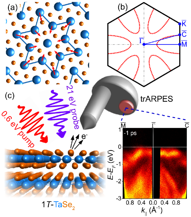
According to previous ARPES investigations arpes1 ; arpes2 ; mott1 , constant binding energy cuts close to the Fermi level reveal large elliptical electron pockets centered at the point of the Brillouin Zone (BZ), as shown in Fig. 1b. Here, we introduce the point which is the midpoint between and , and then focus on the path (blue solid line in Fig. 1b) that maximizes the intersection with these pockets. We demonstrate how this is key for observing the bottom CB. Fig. 1c shows the trARPES experimental layout. Photo-excitation was provided by 0.6 eV pulses with fluence of 3 mJ/cm2 at 1 kHz repetition rate. Photoemission spectra were acquired with 21 eV pulses produced via high harmonic generation in argon, which gives access to the entire first BZ of 1-TaSe2. The overall time and energy resolution of the setup is 90 fs and 200 meV, respectively. The sample was held at 80 K during measurements.
Fig. 2a shows the ARPES maps measured along at selected pump-probe delays.
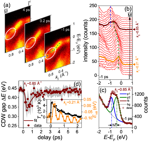
The highest occupied state is the Ta-dominant valence band (VB), which shows a discontinuity, highlighted by dashed ellipses, arising from an avoided crossing due to band folding in the CDW phase (see Supplementary E). At 0.2 ps after the pump (middle map in Fig. 2a) the discontinuity is blurred, but it fully recovers within 4 ps. The energy distribution curves (EDCs) at equally separated momenta along are shown in Fig. 2b for negative pump-probe delay. They reveal a gap at Å-1 (bold brown curve) whose dynamics can be retrieved through a double-peak fitting procedure, as illustrated in Fig. 2c. The peak separation represents the CDW gap faraday and Fig. 2d displays its temporal evolution. It is instructive to compare this with the dynamics observed in the proximity of the Fermi level ( Å-1, bold orange curve in Fig. 2b). Upon laser excitation, electrons from occupied states are promptly driven out of equilibrium. Using the Fermi-Dirac function in the EDCs of the VB at Å-1 (see Supplementary C), the transient electronic temperature is deduced, as reported in the inset of Fig. 2d (black dots). The pulsewidth-limited rise time of the electronic temperature is attributed to electron-electron scattering processes in the VB occurring within the pulse duration (sub- fs). The subsequent cooling is ascribed to electron-phonon interaction with a characteristic scattering time ps. Additionally, a strong coherent phonon oscillation of the VB is observed (see Fig. 2d, orange dots); its frequency THz identifies the so-called breathing mode KM1 ; KM2 ; aom , that is a coherent expansion and contraction of the star triggered by a displacive mechanism displacive , as evidenced by the phase of the oscillations (see Supplementary B). Despite the fact that an intense electronic perturbation is promptly induced by the photoexcitation ( K), only a moderate % reduction of the CDW gap is observed, with its minimum value being reached about 0.3 ps after the optical excitation (Fig. 2d, main panel). Such a response is perfectly compatible with the lattice dynamics, since it matches half the period of the breathing mode ( ps) and dictates the fastest response time of the lattice to an external perturbation. This fact provides clear evidence that the CDW gap is lattice-related and rather robust against electronic perturbations from an optical excitation. Both CDW gap and electronic temperature recover with the same characteristic time constant implying a common mechanism, that is electron-phonon coupling.
We now focus on the central experimental result of this Letter. Fig. 3a shows the band structure of of 1-TaSe2 along the direction as measured by trARPES at selected pump-probe delays (for completeness the full path at 0 ps delay is reported).
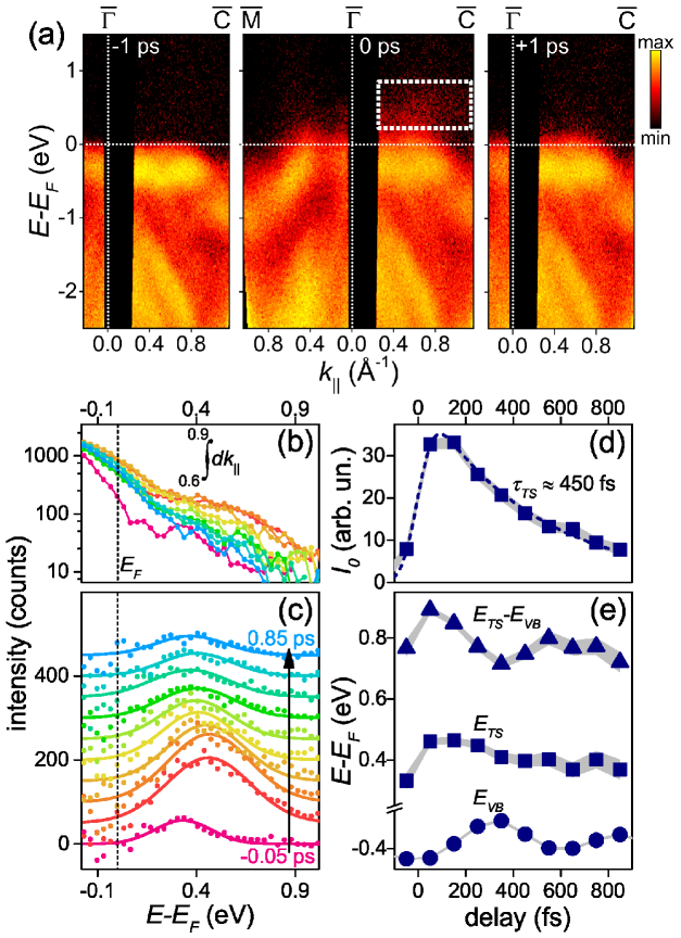
At 0 ps, a transiently populated state (TS) above spanning the probed region can be seen (dashed rectangle), which disappears 1 ps after the optical excitation. This state is hardly observed along . Fig. 3b shows the EDCs measured in the time window between and ps (step of 0.1 ps) and integrated over Å-1. After removing the residual spectral weight extending from the VB above the Fermi level, the TS and its dynamics clearly emerge in Fig. 3c. The solid lines are Gaussian fits from which intensity and binding energy of the TS are extrapolated, respectively in Fig. 3d and Fig. 3e. We find a lifetime fs (Fig. 3d) which is shorter than the electron-phonon scattering time, indicating the presence of additional relaxation and recombination channels. The binding energy of the TS (Fig. 3e) reveals a weak temporal dependence, converging towards the value eV. For comparison, the binding energy of the VB is reported, showing the effect of the coherent phonon oscillation previously discussed. We notice that the peak-to-peak energy separation between TS and VB, , is essentially modulated by the dynamics of the latter. If we were to label VB and TS as the lower and upper Hubbard bands, we would obtain a Coulomb correlation energy of eV. This value is slightly larger, but still compatible with previous investigations 13 ; 14 within our energy resolution (0.2 eV). However, the lifetime of the TS provides a strong indication of its nature. First, it cannot be ascribed to a laser-induced excitation continuum, as it would bear a much shorter lifetime ligges with binding energy rapidly converging towards . On the other hand, it cannot be assigned to a Hubbard-like band: recent trARPES measurements on 1-TaS2 revealed the UHB and its relaxation was estimated to occur on the timescale of electron hopping fs ligges . Given the structural and electronic similarities with 1-TaS2, one would expect a comparable timescale in 1-TaSe2. However, our data reveal a lifetime of the TS which is times longer, rebutting its Mott-like nature. DFT calculations also predict the existence of the TS above the Fermi level with a large spectral weight in the direction, as observed in the experiments, but its origin rests on the specific electronic structure induced by the star-like reconstruction, as clarified in the following.
In the CDW phase there are three types of nonequivalent Ta atoms labeled , and in Fig. 4a, with numerical proportion . Atom (green) lies at the center of the star, atoms (blue) are the nearest neighbors, atoms (red) occupy the tips of the star.
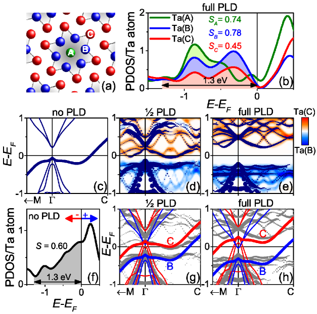
The projected density-of-states (PDOS) in Fig. 4b shows that each atom type has a different electronic occupancy. By integrating the PDOS over the energy range spanned by the highest Ta-dominant VB (from eV to , see Supplementary E), the relative electronic charges are estimated: electrons accumulate towards the center of the star (), depleting the tips () xps . This effect, perfectly consistent with the CDW description, is inherently governed by the electronic band configuration in the charge-ordered phase. Focusing our attention on the path of the BZ, Fig. 4c reports the calculated band structure of the undistorted 1-TaSe2, i.e. with no PLD. The thick line marks the Ta-dominant band with metallic character (as expected in the normal phase), which would split into LHB and UHB in a Mott insulator picture. Fig. 4d shows the unfolded band structure at an intermediate distortion (i.e. 1/2 PLD, see Supplementary E) between the undistorted (Fig. 4c) and the fully-developed CDW phases (Fig. 4e). Panels (c)-(e) track the band evolution with increasing PLD; the Ta band splits into two main replicas, one moving above the Fermi level and a manifold shifting below it. The former, being partially above , hosts fewer electrons than the latter. Based on the charge occupancies inferred from the integrated PDOS (Fig. 4b), we associate the band below to atoms and , while its higher energy equivalent to atoms . This scenario is further supported by atom-specific projections: the band structures in Fig. 4d-e are superimposed to the corresponding contributions of atoms type (inner part of the star) and type (tips of the star) in blue and red color, respectively, confirming that the outer portion of the star hosts the unoccupied states, while the inner part spawns the Ta bands below . In the following, we will exploit the calculated PDOS and electronic occupancies to quantitatively estimate the energy shifts of the two Ta-band replicas arising in the charge-ordered phase. Referring to the undistorted structure (Fig. 4c and 4f) one can notice that a rigid shift of the entire band structure to lower[higher] energy with respect to would result in a larger[smaller] electron occupancy (shifting the entire band structure to positive energy corresponds to moving to negative values). In practice, by moving the Fermi level in Fig. 4f, we can tune the electronic occupancy of the Ta-dominant state in the undistorted lattice to match those of atoms type or in the distorted phases. The corresponding shifted bands are shown in Fig. 4g-h (numerical details for both 1/2 PLD and full PLD cases are given in the Supplementary F). They are superimposed to the respective unfolded band structures (gray dots), revealing a good agreement. In other words, the VB and the TS experimentally observed by trARPES (Fig. 3a) are both Ta-dominant bands originating from different Ta atom types of the star ( and , respectively). Notice that PLD hinders the metallic character, opening a gap across . Although the predicted dispersion of the unoccupied Ta band along (Fig. 4e) cannot be fully probed by our measurements (its bandwidth is comparable to our energy resolution and the pump photon energy of 0.6 eV might not populate it homogeneously) the binding energy determined experimentally matches the computed value well. We point out that our DFT calculations capture all main features of the charge-ordered electronic structure without employing Hubbard correlation terms. Considering the structural and electronic similarities of 1-TaSe2 and 1-TaS2, one may discuss why the Mott phase appears only in the latter. A comparison between their surface-projected band structures in the undistorted phase (Supplementary G) shows (i) a reduced bandwidth of the Ta-dominant band in the sulfide, as compared to the selenide, indicating stronger electron localization in 1-TaS2 which may favor the Mott transition and (ii) hybridization of chalcogen and metal states at in 1-TaSe2, but not in 1-TaS2, suggesting enhanced screening in the selenide which may hinder the Mott phase.
In conclusion, trARPES data reveal that under photoexcitation conditions leading to a considerable increase of the electronic temperature ( eV, Fig. 2d), the induced closure of the CDW gap in the Ta-dominant band is relatively moderate ( eV, Fig. 2d) and established at the lattice level, as evidenced by the gap response time matching half the period of the star breathing mode ( ps, Fig. 2d, inset). This fact suggests that electron-phonon coupling dominates over electronic instabilities in the formation of the CDW, in accordance with previous works KM1 ; insta2 ; epc1 . The results shown in Fig. 3 and Fig. 4 prove that, from a purely electronic viewpoint, when entering the CDW phase, charge migration from the tips towards the center of the star leads to the appearance of a charge-transfer gap rather than a Mott gap chargetr , as corroborated by the temporal evolution of the transiently populated state above seen with trARPES, and by DFT calculations. While we cannot disagree with the fact that monolayer 1-TaSe2 might be a Mott system, our investigation confutes the Mott nature of its bulk counterpart.
We acknowledge financial support from the Italian Ministry of University and Research (grant PRIN 2017BZPKSZ) and LaserLab-Europe (grant agreement no. 871124, European Union’s Horizon 2020 research and innovation programme). Access to Artemis at the Central Laser Facility was provided by STFC (experiment no. 20120002) with technical support from Alistair Cox, Phil Rice and Ota Michalek. Computational work was also supported by the University of Bath Cloud Pilot Project and the EU Horizon 2020 OCRE project ”Cloud funding for research”.
References
- (1) E. Dagotto, Science, 309, 257 (2005).
- (2) D.N. Basov, R.D. Averitt, D. Hsieh, Nature Mater. 16 1077-1088 (2017).
- (3) C.W. Chen, J. Choe, E. Morosan, Rep. Prog. Phys. 79, 084505 (2016).
- (4) J. Chang, E. Blackburn, A.T. Holmes, N.B. Christensen, J. Larsen, J. Mesot, R.X. Liang, D.A. Bonn, W.N. Hardy, A. Watenphul, M. von Zimmermann, E.M. Forgan, S.M. Hayden, Nature Phys. 8, 871-876 (2012).
- (5) H.X. Tan, Y.Z. Liu, Z.Q. Wang, B.H. Yan, Phys. Rev. Lett. 127, 046401 (2021).
- (6) F. Gebhard, The Mott Metal-Insulator Transition (Springer, Heidelberg 1997).
- (7) M. M. Qazilbash, M. Brehm, B.-G. Chae, P.-C. Ho, G. O. Andreev, B.-J. Kim, S. J. Yun, A. V. Balatsky, M. B. Maple, F. Keilmann, H.-T. Kim, D. N. Basov, Science 318, 1750 (2007).
- (8) A. Cavalleri, Th. Dekorsy, H. H. W. Chong, J. C. Kieffer, and R. W. Schoenlein, Phys. Rev. B 70, 161102(R) (2004).
- (9) J.A. Wilson, F.J. Di Salvo, S. Mahajan, Adv. Phys. 24, 117-201 (1975).
- (10) K. Rossnagel, J. Phys. Condes. Matter 23, 213001 (2011).
- (11) P. Fazekas, E. Tosatti, Philos. Mag. B 39, 229-244 (1979).
- (12) D. Shin, N. Tancogne-Dejean, J. Zhang, M.S. Okyay, A. Rubio, N. Park, Phys. Rev. Lett. 126, 196406 (2021).
- (13) L. Perfetti, P.A. Loukakos, M. Lisowski, U. Bovensiepen, H. Berger, S. Biermann, P.S. Cornaglia, A. Georges, M. Wolf, Phys. Rev. Lett. 97, 067402 (2006).
- (14) C. Sohrt, A. Stange, M. Bauera, K. Rossnagel, Faraday Discuss. 171, 243 (2014).
- (15) L. Perfetti, A. Georges, S. Florens, S. Biermann, S. Mitrovic, H. Berger, Y. Tomm, H. Höchst, M. Grioni, Phys. Rev. Lett. 90, 166401 (2003).
- (16) Y. Chen, W. Ruan, M. Wu, S.J. Tang, H.Y. Ryu, H.Z. Tsai, R. Lee, S. Kahn, F. Liou, C.H. Jia, O.R. Albertini, H.Y. Xiong, T. Jia, Z. Liu, J.A. Sobota, A.Y. Liu, J.E. Moore, Z.X. Shen, S.G. Louie, S.K. Mo, M.F. Crommie, Nature Phys. 16, 218 (2020).
- (17) Yuki Nakata, Takuya Yoshizawa, Katsuaki Sugawara, Yuki Umemoto, Takashi Takahashi, Takafumi Sato, ACS Appl. Nano Mater. 1, 1456 (2018).
- (18) Y. Nakata, K. Sugawara, A. Chainani, H. Oka, C. Bao, S. Zhou, P.-Y. Chuang, C.-M. Cheng, T. Kawakami, Y. Saruta, T. Fukumura, S. Zhou, T. Takahashi, T. Sato, Nat. Comm. 12, 5873 (2021).
- (19) S. Colonna, F. Ronci, A. Cricenti, L. Perfetti, H. Berger, M. Grioni, Phys. Rev. Lett. 94, 036405 (2005).
- (20) W. Zhang, Z. Wu, K. Bu, Y. Fei, Y. Zheng, J. Gao, X. Luo, Z. Liu, Y.-P. Sun, Y. Yin, Phys. Rev. B 105, 035110 (2022).
- (21) H. Hedayat, C.J. Sayers, D. Bugini, C. Dallera, D. Wolverson, T. Batten, S. Karbassi, S. Friedemann, G. Cerullo, J. van Wezel, S.R. Clark, E. Carpene, E. Da Como, Phys. Rev. Res. 1, 023029 (2019).
- (22) C.J. Sayers, H. Hedayat, A. Ceraso, F. Museur, M. Cattelan, L.S. Hart, L.S. Farrar, S. Dal Conte, G. Cerullo, C. Dallera, E. Da Como, E. Carpene, Phys. Rev. B 102, 161105 (2020).
- (23) L. Rettig, R. Cortés, J.H. Chu, I.R. Fisher, F. Schmitt, R.G. Moore, Z.X. Shen, P.S. Kirchmann, M. Wolf, U. Bovensiepen, Nat. Comm. 7, 10459 (2016).
- (24) J. A. Wilson, F. J. Di Salvo, S. Mahajan, Phys. Rev. Lett. 32, 882-885 (1974).
- (25) C. Sohrt, A. Stange, M. Bauer, K. Rossnagel, Faraday Discuss. 171, 243 (2014).
- (26) M. Bovet, D. Popović, F. Clerc, C. Koitzsch, U. Probst, E. Bucher, H. Berger, D. Naumović, P. Aebi, Phys. Rev. B 69, 125117 (2004).
- (27) Y. Aiura, H. Bando, R. Kitagawa, S. Maruyama, Y. Nishihara, K. Horiba, M. Oshima, O. Shiino, M. Nakatake, Phys. Rev. B 68, 073408 (2003).
- (28) X. Shi, W. You, Y. Zhang, Z. Tao, P.M. Oppeneer, X. Wu, R. Thomale, K. Rossnagel, M. Bauer, H. Kapteyn, M. Murnane, Sci. Adv. 5, eaav4449 (2019).
- (29) Y. Zhang, X. Shi, W. You, Z. Tao, Y. Zhong, F.C. Kabeer, P. Maldonado, P.M. Oppeneer, M. Bauer, K. Rossnagel, H. Kapteyn, M. Murnane, PNAS 117, 8788 (2020).
- (30) C. J. Sayers, S. Dal Conte, D. Wolverson, C. Gadermaier, G. Cerullo, E. Carpene, E. Da Como, Adv. Optical Mater. 10, 2200362 (2022).
- (31) H. J. Zeiger, J. Vidal, T. K. Cheng, E. P. Ippen, G. Dresselhaus, M. S. Dresselhaus, Phys. Rev. B 45, 768 (1992).
- (32) M. Ligges, I. Avigo, D. Golež, H. U. R. Strand, Y. Beyazit, K. Hanff, F. Diekmann, L. Stojchevska, M. Kalläne, P. Zhou, K. Rossnagel, M. Eckstein, P. Werner, U. Bovensiepen, Phys. Rev. Lett. 120, 166401 (2018)
- (33) D. Wolverson, B. Smith, E. Da Como, C. Sayers, G. Wan, L. Pasquali, M. Cattelan, J. Phys. Chem. C 126, 9135 (2022).
- (34) Y. Ge, A.Y. Liu, Phys. Rev. B 82, 155133 (2010).
- (35) Y. Liu,D. F. Shao, L. J. Li, W. J. Lu, X. D. Zhu, P. Tong, R. C. Xiao, L. S. Ling, C. Y. Xi, L. Pi, H. F. Tian, H. X. Yang, J. Q. Li, W. H. Song, X. B. Zhu, Y. P. Sun, Phys. Rev. B 94, 045131 (2016).
- (36) S. Qiao, X. Li, N. Wang, W. Ruan, C. Ye, P. Cai, Z. Hao, H. Yao, X. Chen, J. Wu, Y. Wang, Z. Liu, Phys. Rev. X 7, 041054 (2017).