Mobility enhancement in CVD-grown monolayer via patterned substrate induced non-uniform straining
Abstract
The extraordinary mechanical properties of 2D TMDCs make them ideal candidates for investigating strain-induced control of various physical properties. Here we explore the role of non-uniform strain in modulating optical, electronic and transport properties of semiconducting, chemical vapour deposited monolayer , on periodically nanostructured substrates. A combination of spatially resolved spectroscopic and electronic properties explore and quantify the differential strain distribution and carrier density on a monolayer, as it conformally drapes over the periodic nanostructures. The observed accumulation in electron density at the strained regions is supported by theoretical calculations which form the likely basis for the ensuing increase in field effect mobility in strained samples. Though spatially non-uniform, the pattern induced strain is shown to be readily controlled by changing the periodicity of the nanostructures thus providing a robust yet useful macroscopic control on strain and mobility in these systems.
Keywords: , nonuniform strain, conducting AFM, mobility enhancement
1 Introduction
Both natural and synthetic two-dimensional (2D) materials have continued to dominate the area of materials research owing to a multitude of fascinating physical properties they exhibit. The relevance of individual materials stem not only from niche properties but the associated control parameters, and especially their accessibility in conducive functional forms e.g., pristine growth and ease of doping, especially in forms that enable incorporation and processing with standard CMOS technologies. The class of semiconducting transition metal dichalcogenides (TMDCs)[1, 2] with strain as a control parameter are particularly relevant in the above context. Strain induced modulation of band structure in atomically thin TMDCs is one of the most elegant methods for engineering their electrical, luminescence, optoelectronic and photonic properties. [3, 4, 5, 6] Monolayer TMDCs posses incredible mechanical strength (in-plane stiffness ), a low bending modulus () along with extreme strain endurance capability (), making them ideal candidates for exploring strain engineering.[7, 8, 9, 10] Introduction of strain in TMDCs break the inversion symmetry, resulting in significant changes in the electronic band structure, lowering the band-gap and transitioning from direct to indirect in monolayer samples, as evidenced in the photoluminescence (PL) properties. [3, 4, 5, 11] Previous investigations have reported various straining mechanisms that includes (i) uniaxial [4, 5, 12], or biaxial straining, [13, 14, 6, 15] (ii) draping over patterned or roughened substrates[16, 17], and through (iii) formation of wrinkles and bubbles or buckle delamination that are nucleated due to differential straining or surface adhesion[18, 19]. Under tensile strain, monolayer shows a reduction in the optical bandgap () under uniaxial strain [4, 5], and for biaxial strain, [6, 20] evidencing upto reduction of .[6] Typically, the changes from direct to indirect for strain beyond , [4, 11] which therefore allow continuous tuning of emission energy and intensities[3, 6]. While stretching and bending of flakes mounted on flexible substrates allow for continuous, uniform and quantifiable control of %strain and enables robust calibration of strain dependent properties, the device architecture are not conducive for simultaneous variation of other parameters like temperature, gating etc. and is not compatible with standard semiconductor device process flow.
Conformal draping of atomically thin flakes onto nanostructured or even roughened substrates offer an alternate straining method that alleviates many of the above shortcomings along with additional advantages, though the non-uniform nature of strain distribution makes its quantification and control more complex. Draping flakes over periodically patterned substrates, as attempted here, nucleates spatially modulated local strain and allows for a degree of control on the overall strain in the flake, via change in geometry and periodicity of the underlying pattern. In such cases, maximum strain is typically induced at the edges of the patterned nanostructures (NS), along with the wrinkles, bubbles and buckling that take place in the intervening regions between the NS, as discussed later. Such spatial localization of strain induces spatially localized modification to both the electronic and phonon band structures, where local reduction in creates local potential wells in the otherwise uniform potential landscape i.e. in the conduction and valence band minima and maxima (CBM and VBM). Local reduction in increases the local electron density (),[21, 22] and under photo-excitation enhances the local PL intensity [23, 24, 25]. The enhancement is aided by the “funnelling” effect [23, 26, 24, 19], where excitons from surrounding regions diffuse and localize at the potential wells, which is also reported to give rise to extremely sharp emission lines () and create single-photon emission centres.[27, 28, 29] Such non-uniform strain has also been shown to increase carrier mobility () and improve device performance in mechanically exfoliated monolayers.[30, 16] The higher mobility also benefits from the associated reduction of the electron effective mass (),[31] and enhanced screening due to the higher thus reducing scattering from charged defects. Further, strain induced local distortion of the atomic lattice potentially modifies the intrinsic dielectric constant () and the phonon density of states, adversely affecting electron-phonon scattering.[16] Together the above parameters would contribute to improvement in carrier mobility and overall electrical transport properties, as reported before.[11, 32, 33]
Here, strain induced change in local optical, electrical and electronic properties of CVD-grown monolayer flakes are investigated by transferring the flakes on to SiO2/Si substrates patterned with periodic Au NS. While spatially resolved PL and Raman spectroscopy evidences the effects of local strain, bearing registry with the underlying NS pattern, the spectral red-shifts quantify the local % strain. Strain induced nanoscale features such as wrinkles, nanobubbles etc. are visualized via atomic force microscopy (AFM) based measurements, which not only resolves these nanoscale features but also provides an alternate route for quantification of local strain, via local curvature of the surface. The spatially resolved current and conductance maps from conducting AFM (CAFM) investigations directly evidences higher at the strained regions by . The results are commensurate with the observed red-shift of the Raman mode that is sensitive to , and corroborated by theoretical calculations that reveal the band diagram at the unstrain – strain interface along with the accumulation of carriers in the strained regions, especially at the interfaces. Finally, field effect transistor (FET) measurements on these strained demonstrates stronger gate modulation of channel conductance, improved channel conductivity and higher carrier mobility (), in comparison to unstrained samples. The increase in is shown to scale with “overall strain” effected via increased NS density.
Overall our results present a comprehensive picture of strain engineering via macroscopic patterning of substrate and the effects of induced modulation in local optical and electronic properties along with electrical transport in CVD-grown monolayer TMDCs. The wide compatibility of the methodology and ease of customization contextualizes the relevance of the present investigation, which is applicable to various fields like photonics, optoelectronics, quantum technologies etc.
2 Results and Discussion
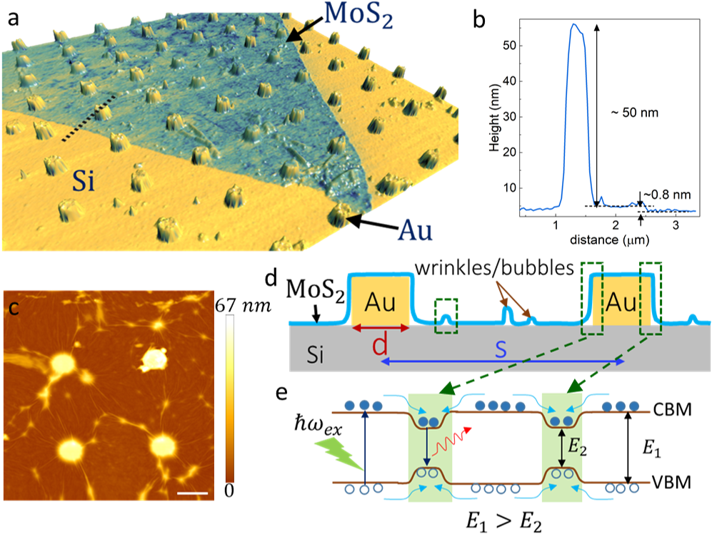
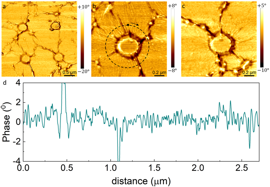
CVD-grown monolayer flakes were transferred onto Si substrates with pre-patterned square periodic array of Au nanocylinders of diameter: , height: and periodicity () varying from to . Details of patterning and sample transfer are available in Supporting Information (SI) section S1. Figure 1a shows the 3D topography of a monolayer flake on a nanostructured substrate with (see SI figure S1). The line scan in figure 1b, along the black-dotted line in figure 1a, reveals the height of the cylindrical NS to be , and the monolayer thickness of . Topographically the flake conformally drapes over the Au NS, nucleating wrinkles that spread out “radially” from each NS along with occasional nanobubble formation in the intervening region, in-between the NS (figure 1c). Figure 1d shows a cross sectional schematic of the flake draped over the NS, with high strain regions demarcated by dashed green lines. The presence of these local perturbations indicate non-uniform, local strain on the flake that distorts the lattice locally, modifying the local electronic bandstructure.[6, 4, 3] Figure 1e shows the schematic band-diagram depicting the variation of conduction and valence band edges (CBM, VBM) across unstrained and strained regions, creating local potential wells and “funnelling” of photogenerated charge carriers from the surrounding regions.
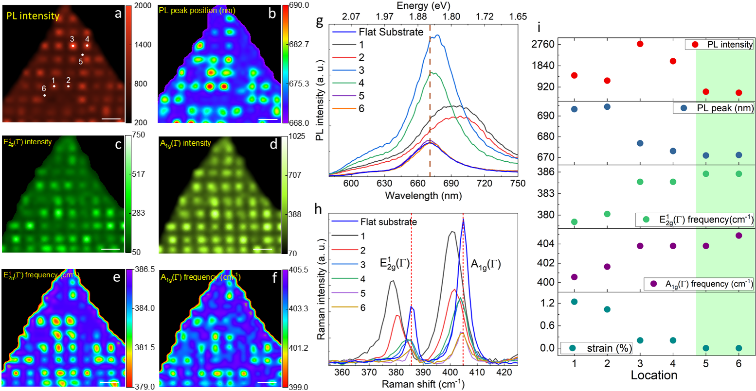
Figure 2a shows the spatial map of the primary PL peak intensity, around corresponding to excitons[34] across the monolayer on the nanostructured substrate. The map bears registry with the underlying pattern (figure 1) with the peak intensity maximizing at regions around the Au NS, designated as “on” points (e.g. points 1, 2, 3 and 4 in figure 2a), compared to the peak intensity from the “off” regions lying between NS (e.g. points 5 and 6). Figure 2b shows the spatial map of the peak emission wavelength () that varies between again bearing registry with the NS periodicity. at the “on” sites are red-shifted between compared to that from the “off” points. Individual PL spectrum acquired at the six points are shown in figure 2g, along with that from an unstrained on a flat surface, for which the is denoted by the brown-dashed line. The higher intensity and red-shifted spectra from the “on” regions reflect the local reduction in bandgap of at the strained regions.
The locally induced strain in the flake is readily evidenced in spatially resolved Raman spectral analysis across the sample and evolution of the two primary modes, i.e. the in-plane and out-of-plane modes may be used to estimate the locally induced strain effectively. The spatial maps of the modal intensity and frequency of the two modes are shown in figures 2c and 2e for and figures 2d and 2f for the mode. For either mode the Raman signal is more intense at the NS (“on” points) that is accompanied by mode softening, with the peaks shifting to lower frequencies. Figure 2h plots the Raman spectra acquired with excitation at the six locations shown in figure 2a. The spectra resolve the two characteristic Raman modes at and ,[6, 25] recorded for on a flat surface matching with those at the “off” points (5 and 6) shown by red-dotted lines in figure 2h. At the “on” sites (points 1 – 4) the mode shows variable red-shift upto , which for the mode is red-shifted upto . While the red-shift in arises from local strain,[4] that of is influenced by local [21] and provides a relative measure of the same. Thus, the corresponding spatial maps in figures 2e and 2f demarcates regions of high and low strain and , respectively. The correlation between the PL and Raman maps is indicative of the common origin, i.e. strain, of either phenomena as elucidated in figure 2i which co-plots the peak PL intensity, along with the frequency of the and modes across the six “on-off” locations in figure 2a. The PL spectra at points 1 and 2 show the greatest red-shift, commensurate with the highest red-shift of the Raman modes, signifying high strain and . The figure also plots the strain values in the range to , estimated from the red-shift in peak, following ref[6].
Similarly, the spectral red-shift of the peak (figure 2f) over NS varies in the range of to , indicating increased yet non-uniform local doping across the strained regions. Strain induced reduction in bandgap (red-shift in the PL spectrum) has been reported to be strain for uniaxial tensile strain[4] and under biaxial strain.[6, 20] Consequently, a red-shift in , at points 1 and 2 correspond to strain between depending on the uniaxial or biaxial nature of the local strain. Similarly, PL spectra from positions 3 and 4 show less red-shift in (bandgap lowering ), with lower estimated strain () and high PL peak intensity enhancement () compared to the unstrained regions, due to the “funnelling” effect. The lower PL enhancement () at the more strained points 1 and 2 is due to the more indirect nature of the bandgap, along with increased spectral broadening (figure 2g), indicating phonon-assisted indirect processes contributing to the spectra [6, 4, 3, 35, 36] (see SI section S3 for further discussion).
Overall, these observations indicate strain-induced modification in local bandstructure of , especially bandgap reduction at the NS, which is schematically represented in figure 1e. This leads to local lowering of the CBM at the strained regions creating potential wells, spatially modulating the potential landscape, which leads to “funnelling” of excitons towards local potential minima (figure 1e). [3, 27, 25] As a result, strained regions in exhibit enhanced PL intensity in comparison to unstrained regions. CVD-grown monolayers are known to be -type doped and the additional lowering of the band gap at strained regions increases the probability of thermal excitation and defect ionization, thus increasing the local carrier density that is reflected in the correlated frequency shift at the strained regions evidenced in figures 2i and 2f.
Though the spectroscopic signatures of localized strain around the NS in the corresponding spatial maps, they lack adequate resolution to evidence strain effects on the smaller features i.e., the wrinkles and bubbles, which are well resolved in AFM results.
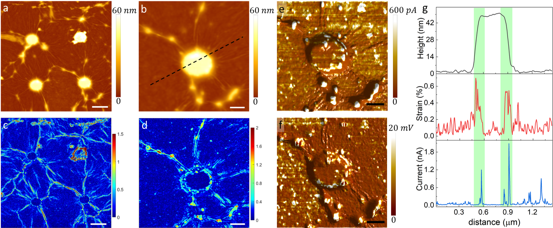
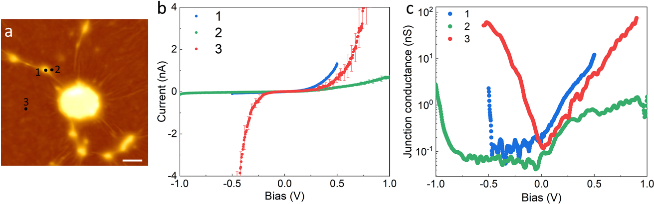
Figures 3a and 3b show large and small area AFM topography of the NS draped with an flake resolving the wrinkles and nanobubbles. The wrinkles, extending “radially” outward from each NS are high strain features that allow relaxation of strain in the “flat” regions between the NS. The features visualized with clarity in the AFM phase images shown in figure S2 in SI. Figures 3c, d display the map of the component of the strain tensor, calculated from the topographic map (figures 3a, b), using continuum elasticity theory [37] using the equation:
| (1) |
where, denotes the Poisson’s ratio [10] and is the thickness of monolayer and represents the local topographic height variation in the sample. The maps (figures 3c, d) not only demarcate and quantify strain in at the NS edges, but also accentuate the strain along the wrinkles and nanobubbles. Other intervening regions, including the top of the NS show negligible strain. The estimated %strain lie in the range: , which is commensurate with the strain values obtained from the Raman and PL spectral shifts. Table S1 in SI tabulates and compares the estimated %strain values from the red-shift in the PL spectra, Raman spectral shift and calculated from the AFM topography.
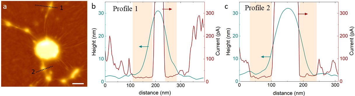
The effects of change in bandstructure is also reflected in the local electrical and electronic properties of the strained regions. Figures 3e and 3f depicts the spatially resolved conducting AFM current map and the junction maps at sample bias, recorded simultaneously with the topography shown in figure 3b. Both the current and maps display high tip-sample current and local conductance over the high strained regions located at the periphery of NS, over the wrinkles and at the nanobubbles, that are correlated with features in the strain map (figure 3d). The correlations are better visualized in the line scans in figure 3g, taken along the black-dashed line shown in figure 3b. The green shaded region in figure 3g denotes the edge of the NS wherein the is maximally strained and carries high current. Similar observations have been reported in tunnelling spectroscopy,[38, 39] measurements that evidence local increase in carrier density and higher conductance in strained . This is commensurate with the observed softening of the Raman modes at the strained regions, with higher local . The current and maps also show that the regions between the NS carry lower current and local conductance (figure 3e, f). The variation is better probed through point and spectra shown in SI figures S3b and S3c, which are recorded at different locations marked in the accompanying topography (figure S3a). The and spectra recorded over a nanobubble (location: 1, blue) shows higher junction current and local conductance, compared to the spectra recorded over flat region (location: 3, red). The spectra recorded at the periphery of the strained regions (location: 2) shows the lowest current and conductance, which is indicative of local depletion in carriers. Carrier depletion at the periphery of strained regions is also evident in current map (figure 3e), map (figure 3f) and the correlated linescans in figure S4 in SI, taken across multiple wrinkles, which are regions of high strain.
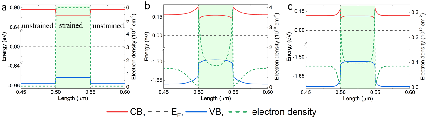
The contrast in the current and conductance maps, recorded across the unstrained and strained regions of is better comprehended through the calculated energy band diagram in the cross-over region. The band diagrams were calculated employing finite element method to solve the Poisson equation using COMSOL Multiphysics 5.3a.
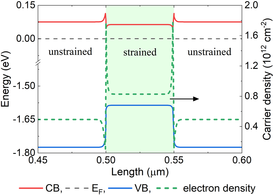
Figure 4 plots a simulated band profile for a 1-dimensional model of , across unstrained-strained-unstrained regions along with the variation in local electron density, calculated at , with intrinsic -type doping . SI section S8 details the geometry and physical parameters used in the model calculation. Figure S6 in SI plots the band diagram and variation in for other doping densities. The conduction (red) and valence (blue) band edges bend across the interfaces creating a local potential well over the strained region, with reduced band gap. For the conduction band edge, the interface is demarcated by a small depletion barrier of width and height on the unstrained part and an accumulation region in the strained region. The calculated (green dashed line) varies between over the strained region, maximizing at accumulation region. Depletion at the peripheral unstrained regions shows a local dip in , which saturates away from the interface. These results are commensurate with the features of the current and conductance maps in figure 3 and those reported earlier. [3, 25, 38, 39] Given the above band alignment, electron-hole pairs generated under optical illumination will be “funnelled” into the strain induced potential wells thereby localizing excitons and aiding PL intensity, as reported.
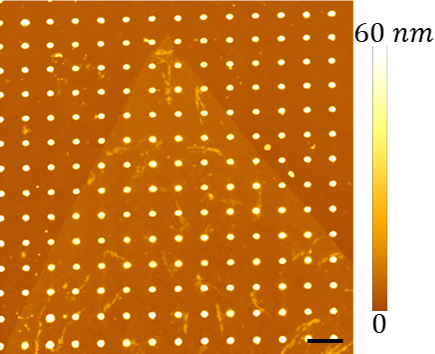
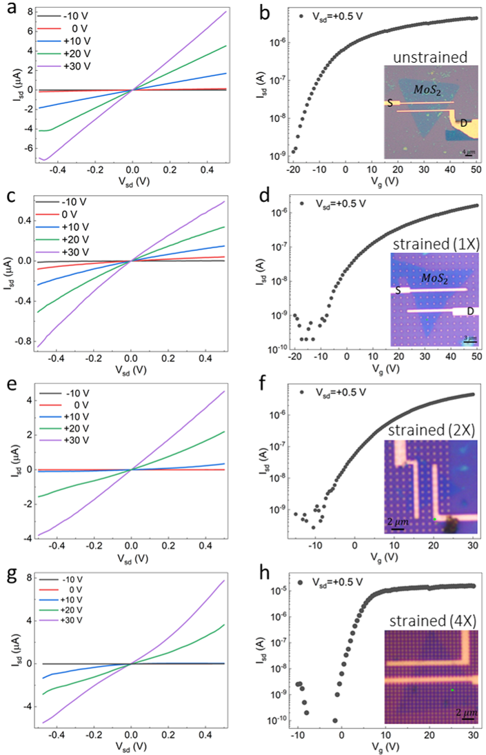
Under conformal draping of flakes over the NS, strain induced effects extend beyond the edge of the NS to intervening regions as wrinkles and nanobubbles, thereby making the whole flake non-uniformly strained. Along with increase in local carrier density, non-uniform strain has been shown to affect overall electrical transport along the 2D flakes, which was investigated here by characterizing FET devices fabricated using unstrained and strained samples, in bottom gate configuration (see section S1 in SI for device architecture). Overall strain in the samples was increased by increasing the density of the NS by reducing their spacing as , and , with the corresponding FET devices labeled as , and strained, respectively. Higher NS density also increases the density of wrinkles and nanobubbles, as shown earlier (figures 1, 3 and figure S2 in SI), which extend radially outward from each NS creating a 2-dimensional network among themselves, covering the entire flake surface, and are interspersed with occasional nanobubbles. These secondary strain features induce local strain throughout the flake. However, exact quantification of %strain across the samples remain non-trivial due to the non-uniform nature of strain distribution. Though the local %strain variation does not change across the samples, “overall strain” in the flake does increase with NS density.
Figure S7 in SI shows the room temperature FET-characteristics, for the unstrained and strained (, , ) devices. All the source-drain characteristics () in figures S6a, c, e and g exhibit “linear” behaviour in the bias range, indicating negligible impact of Schottky barrier at the contacts, at room temperature. The transfer characteristics () in figures S6b, d, f and h show gate bias () dependent channel switching behavior, with ‘on-off’ ratio and exhibit -type channel conductance originating from the native point defects.[40] Figures 5a and 5b plot the variation in the two-probe channel conductivity () and field-effect mobility () calculated from the transfer characteristics, across the four devices. The plots show increasingly stronger modulation of with positive and enhanced with increasing strain in the flake, following the increase in density of nanostructures.
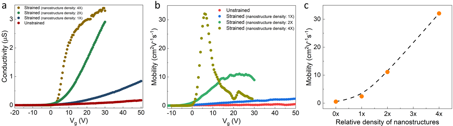
Variation of , calculated from the differential transconductance , for each device is shown in figure 5c (see SI section S10 for details). , which for the unstrained , increases to for the strained sample, for the strained sample and for the strained sample.
Table S3 in SI section S11 summarizes the most significant reports of non-uniform strain induced enhancement reported in literature. The highest for the 4 device is lower than the highest value reported for both exfoliated ()[16] and CVD-grown ()[17] , it is in the ballpark of the latter. The highly non-uniform architecture employed by Huang et al. [17] using underlying metal nanoparticles to locally induce strain in flakes precludes %strain quantification and thus direct comparison with the present devices. However, considering the nanoparticle size employed and the rms roughness, it is fair to conclude that the device had significantly more strain than that in the present 4 device. Therefore it is not surprising that the maximum mobility reported in their device is slightly higher than the 4 device presented here. Nevertheless, the present results (figure 5b, c) show systematic enhancement with strain, which crosses for the most strained device, compared to unstrained and is the highest enhancement reported for CVD-grown flakes and comparable to that for exfoliated ones, as evident from data in table S3.
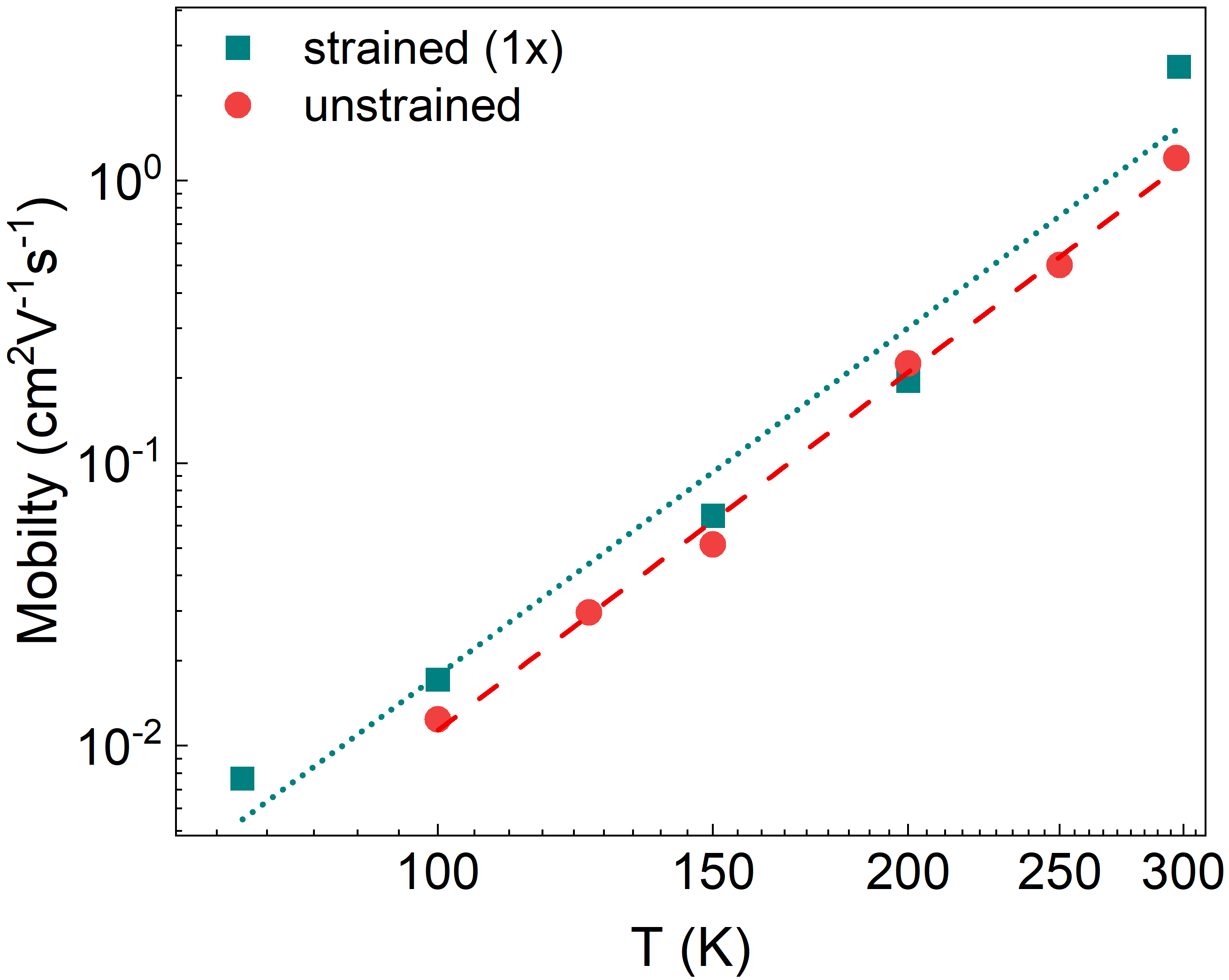
Contrary to transport across exfoliated [16, 41] which is dominated by phonon scattering near room temperature, transport in CVD-grown , with its high native defect density, the presence of sample-substrate interfacial charge impurities and surface adsorbates, is dominated by screened Coulomb interaction mediated scattering. [42, 43, 44, 45, 46] Importantly, CVD-grown samples, including the present case all show comparable that is typically smaller than that of mechanically exfoliated samples. Temperature dependence of is useful in delineating between phonon and charged impurity limited scattering mechanisms. Figure S8 in SI shows plots for the unstrained and strained devices. Both show monotonic decrease of with lowering temperature following a power law , yielding . The positive value of indicates that electrical transport in both strained and unstrained devices are primarily limited by charge-impurity scattering, within the explored range. [44, 42, 16] The decrease in the free electron density, with lowering temperature weakens screening of the charged impurity potential thereby increasing electron-impurity and electron-defect scattering, which in turn suppresses . Further, it has been reported that biaxial strain-induced lattice distortion leads to quenching of the phonon density of states along with an increase in the local dielectric constant, [16] and reduce the effective mass of electrons,[32, 31] all of which would contribute to increase in as observed here.
3 Conclusions
To summarize, we have demonstrated locally non-uniform strain-induced enhancement and control of carrier mobility in CVD-grown monolayer FET devices. Visualization of spatial modulation of local spectroscopic and electronic properties allow in depth comprehension of the phenomena, which shows that electrical transport in these flakes are limited by charged impurity scattering that benefits from increase in carrier density and related effects in the differentially strained devices. Importantly, the substrate NS induced strain control scheme demonstrated here is scalable and provides a straight forward strain control parameter that is crucial for engineering device functionality, and compatible with existing on-chip processing technology for incorporation in standard electronic devices.
Acknowledgement
Authors acknowledge Prof. M M Shaijumon and Dr. Vinayak B. Kamble (IISER Thiruvananthapuram) for use of experimental facilities. JM acknowledges financial support from SERB, Govt. of India (CRG/2019/004965), UGC-UKIERI 184-16/ 2017 (IC) and Newton Bhabha Fund, UK (IAPPI 77). AK acknowledges the PhD fellowship from IISER Thiruvananthapuram. HG and SD acknowledges DST INSPIRE for the PhD fellowship. RN is grateful to University grants commission (UGC), Government of India, for the financial support.
Authors’ contribution
AK, SD, HG performed the experiments, SC conducted the simulations and RN did CVD-growth of samples. AK and JM wrote the manuscript with inputs from all the authors.
Notes
The authors declare no competing financial interest.
Supporting Information (SI)
S1 Experimental Methods
S1.1 Substrate patterning:
The Au-nanostructures of diameter: , height: and varying center to center distance or periodicity: , were fabricated on and Si wafer using standard e-beam lithography pattering with PMMA as the resist using a Raith Pioneer 2 electron beam system. Metal deposition of Cr/Au (, ) was done using a thermal evaporator, followed by standard lift-off using acetone.
S1.2 Sample growth and transfer:
The samples were grown using chemical vapour deposition (CVD) technique using and S-powder as precursor. powder was spin-coated on /Si substrate after dissolving in ethanol and kept inside a quartz tube and placed at the center heating zone of the furnace. S-powder was kept at the upstream end of the tube. Samples growth happened at under continuous Argon flow at . The as-grown flakes on /Si substrate were transferred onto various substrate by wet etching technique. First, the as-grown flakes were coated with 120K PMMA (dissolved in anisole at ), followed by baking at for mins. The coated substrates were floated on 2M aqueous NaOH solution at , to etch out the layer and detach the flakes from substrate into the PMMA film. Later, the detached film was scooped and transferred into water bath for -cycles with a duration of mins for each. The film was transferred by scooping it from water bath with the relevant substrate and subsequently baked at for hr to evaporate the water. Finally, the flakes were obtained after dissolving the PMMA layer in warm acetone, followed by IPA wash and blow dried with air.
S1.3 Spectroscopic study:
The spatially resolved photo-luminescence and Raman studies were conducted using a HORIBA Xplora Plus Raman setup based on a confocal microscope. Raman mapping and spectra acquisition were done with laser excited through a objective with NA: . Spectra for PL and Raman were recorded with TE-cooled () CCD, using grating with ruling density of , and , respectively. All the spectroscopic measurements were conducted in room temperature.
S1.4 Atomic Force Microscopy investigations:
All the AFM investigations were conducted using a Bruker Multimode 8 AFM under ambient conditions. The conducting AFM current maps and -maps were recorded using the TUNA 2 pre-amplifier, having variable voltage gain and capable of detecting current in the range of . Both the current-map and -maps were recorded simultaneously with topography using gold-coated probes (HQ:CSC37/Cr-Au, ) from MikroMasch. For all CAFM maps, bias was applied to the sample, while probe was kept at virtual ground potential.
S1.5 Field Effect Transistor Device Fabrication and Transport measurements:
The FET devices were fabricated on -Si substrate coated with thick, thermally grown layer, which served as the gate dielectric. The source-drain contacts were patterned using e-beam lithography, followed by thermal deposition of Cr/Au (). The transistor characteristics were measured using KEYSIGHT B2902B dual channel source-meter. The low-temperature measurements were conducted inside a closed-cycle He-cryostat (ARS Inc.).
S2 AFM topography of transferred flake
S3 Discussion on change in PL characteristics with strain
Previous investigations show that the momentum and energy of the conduction and valence band minima (CBM, VBM), which are located at the points in the space for monolayer , changes as a function of tensile strain and the nature of the bandgap evolves from direct to indirect.[4, 3, 35] According to Steinhoff et al. [35], smaller values of biaxial tensile strain () retains the direct nature of the bandgap while it’s magnitude reduces due to downshift of the CBM and unchanged VBM at . Experimentally, this results in an increase in PL intensity with commensurate red-shift in emission peak. However, for higher tensile strain (), the VB energy at -point increases above the its value at the -point, consequently the bandgap becomes indirect and the optical transitions are dominated by phonon-assisted processes, which in turn reduces the PL intensity. The initial rise in PL intensity under tensile strain is then understood to arise from nonequilibrium distribution of carriers predominantly in the -valleys, which leads to strong emission from the -exciton decay. The results presented here in figure 2 show similar behavior, PL spectra from positions 3 and 4, with lower strain () show less red-shift () and highest PL peak intensity. The higher strained regions (points 1 and 2) with strain show red-shifted by with reduced intensity due to the more indirect nature of the bandgap [6, 4, 3], along with increased spectral broadening, indicating phonon-assisted indirect processes contributing to the spectra. [35, 36]
S4 AFM phase map
S5 Local and -characteristics
Comparison of the and -characteristics across the three points shows that the strained region (point 1) carries the highest current and shows highest , whereas the immediately adjoining regions at the edge of the strained region (point 2) shows the lowest values, under positive bias. Regions away from the regions of high strain (point 3) show intermediate values.
S6 Correlated Linescans
The correlated line scans in figures S4b and c, between topography and current maps show that the current at the top of high strain region at the nanobubble is the highest (saturated for the current amplifier gain used).The color-shaded regions in the plots demarcate the lowest current carrying regions that surround the high strain nanobubble region. This low current in these surrounding regions denotes local carrier depletion, arises due to strain induced bandgap modulation and band-bending across the interface of strained-unstrained .
S7 Comparison of estimated strain from PL, Raman and AFM study
| Probe | Observed shift | Estimated strain (%) |
|---|---|---|
| PL | ||
| Raman | ||
| AFM |
S8 Simulating the energy band diagram across strained-unstrained interface
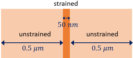
To numerically calculate the band profile at the interfaces of alternating unstrained-strained-unstrained regions of , finite element method modelling was performed using COMSOL Multiphysics 5.3a. A 1D simulation domain as shown in figure S6 was divided into 3 regions, with the middle strained region of width and under 2% strain, while the unstrained regions were taken to be wide.
The physical parameters used to model the strained and unstrained regions are tabulated in table S2.
| property | unstrained | strained |
|---|---|---|
| width (nm) | ||
| relative permittivity | [47] | |
| Strain (%) | ||
| Bandgap (eV) | ||
| Electron affinity (eV) | [48] | |
| effective mass | [32] | |
| doping concentration () | , , , | |
| dopant ionization energy (eV) | ||
All calculations were performed at finite temperature and no variation to background relative permittivity due to strain was incorporated. Following the perturbation theory [49] the effective mass of the unstrained and strained regions are obtained as and , respectively [32, 31] which also affects the ionization energies of the dopant states which are calculated employing the “hydrogenic impurity model” [42]. The energy band diagrams for the composite system for various dopant densities () are shown in the figure below. Previous reports show that is -type doped with typical electron density .[50]
S9 FET characteristics
S10 Mobility Calculation
Field-effect mobility was calculated using the formula:
| (S1) |
where, is oxide layer thickness, denotes vacuum permittivity, is dielectric constant of , and , are channel length and width, respectively. The values were calculated from two-probe FET characteristics and are known to be limited by the nature of the electrical contacts. High contact resistance values lead to underestimating the value of . [51] The linear nature of the source-drain characteristics in the present devices suggest minimal influence of contact resistance in the estimated mobility values. [52]
S11 Comparison of mobility enhancement with strain
| sample | strain | reference | ||
|---|---|---|---|---|
| 1L (CVD) | uniform tensile | [53] | ||
| 1L (CVD) | non-uniform (max) | [17] | ||
| 1L (CVD) | non-uniform | present work | ||
| 1L (exfoliated) | non-uniform | [16] | ||
| 2L (exfoliated) | non-uniform | [16] | ||
| 1L (exfoliated) | non-uniform | [30] | ||
| 1L (exfoliated) | non-uniform | [30] | ||
| 1L (exfoliated) | non-uniform | [30] |
S12 Temperature-dependent mobility
References
- [1] Andrea Splendiani et al. “Emerging photoluminescence in monolayer ” In Nano Letters 10.4, 2010, pp. 1271–1275 DOI: 10.1021/nl903868w
- [2] Zhiyong Y Zhu, Yingchun C Cheng and Udo Schwingenschlögl “Giant spin-orbit-induced spin splitting in two-dimensional transition-metal dichalcogenide semiconductors” In Physical Review B 84.15, 2011, pp. 153402 DOI: 10.1103/PhysRevB.84.153402
- [3] Ji Feng, Xiaofeng Qian, Cheng-Wei Huang and Ju Li “Strain-engineered artificial atom as a broad-spectrum solar energy funnel” In Nature Photonics 6.12, 2012, pp. 866–872 DOI: 10.1038/nphoton.2012.285
- [4] Hiram J Conley et al. “Bandgap engineering of strained monolayer and bilayer ” In Nano Letters 13.8, 2013, pp. 3626–3630 DOI: 10.1021/nl4014748
- [5] Keliang He, Charles Poole, Kin Fai Mak and Jie Shan “Experimental demonstration of continuous electronic structure tuning via strain in atomically thin ” In Nano Letters 13.6, 2013, pp. 2931–2936 DOI: 10.1021/nl4013166
- [6] David Lloyd et al. “Band gap engineering with ultralarge biaxial strains in suspended monolayer ” In Nano Letters 16.9, 2016, pp. 5836–5841 DOI: 10.1021/acs.nanolett.6b02615
- [7] Simone Bertolazzi, Jacopo Brivio and Andras Kis “Stretching and breaking of ultrathin ” In ACS Nano 5.12, 2011, pp. 9703–9709 DOI: 10.1021/nn203879f
- [8] Qing Peng and Suvranu De “Outstanding mechanical properties of monolayer and its application in elastic energy storage” In Physical Chemistry Chemical Physics 15.44 Royal Society of Chemistry, 2013, pp. 19427–19437
- [9] Jin-Wu Jiang, Zenan Qi, Harold S Park and Timon Rabczuk “Elastic bending modulus of single-layer molybdenum disulfide (): finite thickness effect” In Nanotechnology 24.43 IOP Publishing, 2013, pp. 435705
- [10] Kai Liu et al. “Elastic properties of chemical-vapor-deposited monolayer , , and their bilayer heterostructures” In Nano Letters 14.9, 2014, pp. 5097–5103 DOI: 10.1021/nl501793a
- [11] Sheng Yu et al. “Phase transition, effective mass and carrier mobility of monolayer under tensile strain” In Applied Surface Science 325 10.1016/j.apsusc.2014.11.079, 2015, pp. 27–32
- [12] Yanlong Wang et al. “Strain-induced direct–indirect bandgap transition and phonon modulation in monolayer ” In Nano Research 8.8, 2015, pp. 2562–2572 DOI: 10.1007/s12274-015-0762-6
- [13] Jae-Pil So et al. “Electrically driven strain-induced deterministic single-photon emitters in a van der Waals heterostructure” In Science Advances 7.43, 2021, pp. eabj3176 DOI: 10.1126/sciadv.abj3176
- [14] Hyeongwoo Lee et al. “Drift-dominant exciton funneling and trion conversion in 2D semiconductors on the nanogap” In Science Advances 8.5, 2022, pp. eabm5236 DOI: 10.1126/sciadv.abm5236
- [15] Riccardo Frisenda et al. “Biaxial strain tuning of the optical properties of single-layer transition metal dichalcogenides” In npj 2D Materials and Applications 1.1 10.1038/s41699-017-0013-7, 2017, pp. 1–7
- [16] Hong Kuan Ng et al. “Improving carrier mobility in two-dimensional semiconductors with rippled materials” In Nature Electronics 5.8, 2022, pp. 1–8 DOI: 10.1038/s41928-022-00777-z
- [17] Zheng Huang et al. “Large-Scale Ultrafast Strain Engineering of CVD-Grown Two-Dimensional Materials on Strain Self-Limited Deformable Nanostructures toward Enhanced Field-Effect Transistors” In Nano Letters 22.18, 2022, pp. 7734–7741 DOI: 10.1021/acs.nanolett.2c01559
- [18] Shikai Deng, Songwei Che, Rousan Debbarma and Vikas Berry “Strain in a single wrinkle on an flake for in-plane realignment of band structure for enhanced photo-response” In Nanoscale 11.2, 2019, pp. 504–511 DOI: 10.1039/C8NR05884A
- [19] Thomas P Darlington et al. “Imaging strain-localized excitons in nanoscale bubbles of monolayer at room temperature” In Nature Nanotechnology 15.10, 2020, pp. 854–860 DOI: 10.1038/s41565-020-0730-5
- [20] Gerd Plechinger et al. “Control of biaxial strain in single-layer molybdenite using local thermal expansion of the substrate” In 2D Materials 2.1, 2015, pp. 015006 DOI: 10.1088/2053-1583/2/1/015006
- [21] Biswanath Chakraborty et al. “Symmetry-dependent phonon renormalization in monolayer transistor” In Physical Review B 85.16, 2012, pp. 161403 DOI: 10.1103/PhysRevB.85.161403
- [22] Julien Chaste et al. “Intrinsic properties of suspended on pillar arrays for nanomechanics and optics” In ACS nano 12.4, 2018, pp. 3235–3242 DOI: 10.1021/acsnano.7b07689
- [23] Anastasia V Tyurnina et al. “Strained bubbles in van der Waals heterostructures as local emitters of photoluminescence with adjustable wavelength” In ACS Photonics 6.2, 2019, pp. 516–524 DOI: 10.1021/acsphotonics.8b01497
- [24] Jubok Lee et al. “Switchable, tunable, and directable exciton funneling in periodically wrinkled ” In Nano Letters 21.1, 2020, pp. 43–50 DOI: 10.1021/acs.nanolett.0c02619
- [25] Hong Li et al. “Optoelectronic crystal of artificial atoms in strain-textured molybdenum disulphide” In Nature Communications 6.1, 2015, pp. 1–7 DOI: 10.1038/ncomms8381
- [26] Andres Castellanos-Gomez et al. “Local strain engineering in atomically thin ” In Nano Letters 13.11, 2013, pp. 5361–5366 DOI: 10.1021/nl402875m
- [27] Artur Branny, Santosh Kumar, Raphaël Proux and Brian D Gerardot “Deterministic strain-induced arrays of quantum emitters in a two-dimensional semiconductor” In Nature Communications 8.1, 2017, pp. 1–7 DOI: 10.1038/ncomms15053
- [28] Kamyar Parto, Shaimaa I Azzam, Kaustav Banerjee and Galan Moody “Defect and strain engineering of monolayer enables site-controlled single-photon emission up to 150 K” In Nature Communications 12.1, 2021, pp. 1–8 DOI: 10.1038/s41467-021-23709-5
- [29] Johannes Kern et al. “Nanoscale positioning of single-photon emitters in atomically thin ” In Advanced Materials 28.33, 2016, pp. 7101–7105 DOI: 10.1002/adma.201600560
- [30] Tao Liu et al. “Crested two-dimensional transistors” In Nature Nanotechnology 14.3, 2019, pp. 223–226 DOI: 10.1038/s41565-019-0361-x
- [31] Liang Dong et al. “Theoretical study on strain induced variations in electronic properties of 2 H- bilayer sheets” In Applied Physics Letters 104.5, 2014, pp. 053107 DOI: 10.1063/1.4863827
- [32] Won Seok Yun et al. “Thickness and strain effects on electronic structures of transition metal dichalcogenides: 2H- semiconductors (M= Mo, W; X= S, Se, Te)” In Physical Review B 85.3, 2012, pp. 033305 DOI: 10.1103/PhysRevB.85.033305
- [33] Naoki Harada, Shintaro Sato and Naoki Yokoyama “Computational study on electrical properties of transition metal dichalcogenide field-effect transistors with strained channel” In Journal of Applied Physics 115.3, 2014, pp. 034505 DOI: 10.1063/1.4861726
- [34] Kin Fai Mak et al. “Atomically thin : a new direct-gap semiconductor” In Physical Review Letters 105.13, 2010, pp. 136805 DOI: 10.1103/PhysRevLett.105.136805
- [35] A Steinhoff et al. “Efficient excitonic photoluminescence in direct and indirect band gap monolayer ” In Nano Letters 15.10, 2015, pp. 6841–6847 DOI: 10.1021/acs.nanolett.5b02719
- [36] Iris Niehues et al. “Strain control of exciton–phonon coupling in atomically thin semiconductors” In Nano Letters 18.3, 2018, pp. 1751–1757 DOI: 10.1021/acs.nanolett.7b04868
- [37] Lev Davidovich Landau et al. “Theory of elasticity: volume 7” Elsevier, 1986
- [38] Bong Gyu Shin et al. “Indirect bandgap puddles in monolayer by substrate-induced local strain” In Advanced Materials 28.42, 2016, pp. 9378–9384 DOI: 10.1002/adma.201602626
- [39] Sara Shabani et al. “Ultralocalized Optoelectronic Properties of Nanobubbles in 2D Semiconductors” In Nano Letters 22.18 ACS Publications, 2022, pp. 7401–7407
- [40] Wu Zhou et al. “Intrinsic structural defects in monolayer molybdenum disulfide” In Nano Letters 13.6, 2013, pp. 2615–2622 DOI: 10.1021/nl4007479
- [41] Branimir Radisavljevic and Andras Kis “Mobility engineering and a metal–insulator transition in monolayer ” In Nature Materials 12.9, 2013, pp. 815–820 DOI: 10.1038/nmat3687
- [42] Simon M Sze and Kwok K Ng “Physics of semiconductor devices” John wiley & sons, 2006
- [43] Nengjie Huo et al. “High carrier mobility in monolayer CVD-grown through phonon suppression” In Nanoscale 10.31, 2018, pp. 15071–15077 DOI: 10.1039/C8NR04416C
- [44] Zhihao Yu et al. “Towards intrinsic charge transport in monolayer molybdenum disulfide by defect and interface engineering” In Nature Communications 5.1, 2014, pp. 1–7 DOI: 10.1038/ncomms6290
- [45] Subhamoy Ghatak, Atindra Nath Pal and Arindam Ghosh “Nature of electronic states in atomically thin field-effect transistors” In ACS Nano 5.10, 2011, pp. 7707–7712 DOI: 10.1021/nn202852j
- [46] Yi-Hsien Lee et al. “Synthesis of large-area atomic layers with chemical vapor deposition” In Advanced Materials 24.17, 2012, pp. 2320–2325 DOI: 10.1002/adma.201104798
- [47] Ashok Kumar and PK Ahluwalia “Tunable dielectric response of transition metals dichalcogenides (M= Mo, W; X= S, Se, Te): Effect of quantum confinement” In Physica B: Condensed Matter 407.24, 2012, pp. 4627–4634 DOI: 10.1016/j.physb.2012.08.034
- [48] Chenxi Zhang et al. “Systematic study of electronic structure and band alignment of monolayer transition metal dichalcogenides in Van der Waals heterostructures” In 2D Materials 4.1, 2016, pp. 015026 DOI: 10.1088/2053-1583/4/1/015026
- [49] YU Peter and Manuel Cardona “Fundamentals of semiconductors: physics and materials properties” Springer Science & Business Media, 2010
- [50] Hao Qiu et al. “Hopping transport through defect-induced localized states in molybdenum disulphide” In Nature communications 4.1 Nature Publishing Group UK London, 2013, pp. 2642
- [51] Hsiao-Yu Chang, Weinan Zhu and Deji Akinwande “On the mobility and contact resistance evaluation for transistors based on or two-dimensional semiconducting atomic crystals” In Applied Physics Letters 104.11, 2014, pp. 113504 DOI: 10.1063/1.4868536
- [52] Joseph R Nasr et al. “Mobility deception in nanoscale transistors: an untold contact story” In Advanced Materials 31.2, 2019, pp. 1806020 DOI: 10.1002/adma.201806020
- [53] Isha M. Datye et al. “Strain-Enhanced Mobility of Monolayer ” In Nano Letters 22.20, 2022, pp. 8052–8059 DOI: 10.1021/acs.nanolett.2c01707