Epitaxial van der Waals heterostructures of Cr2Te3 on 2D materials
Abstract
Achieving large-scale growth of two-dimensional (2D) ferromagnetic materials with high Curie temperature () and perpendicular magnetic anisotropy (PMA) is highly desirable for the development of ultra-compact magnetic sensors and magnetic memories. In this context, van der Waals (vdW) Cr2Te3 appears as a promising candidate. Bulk Cr2Te3 exhibits strong PMA and a of 180 K. Moreover, both PMA and might be adjusted in ultrathin films by engineering composition, strain, or applying an electric field. In this work, we demonstrate the molecular beam epitaxy (MBE) growth of vdW heterostructures of five-monolayer quasi-freestanding Cr2Te3 on three classes of 2D materials: graphene (semimetal), WSe2 (semiconductor) and Bi2Te3 (topological insulator). By combining structural and chemical analysis down to the atomic level with ab initio calculations, we confirm the single crystalline character of Cr2Te3 films on the 2D materials with sharp vdW interfaces. They all exhibit PMA and close to the bulk Cr2Te3 value of 180 K. Ab initio calculations confirm this PMA and show how its strength depends on strain. Finally, Hall measurements reveal a strong anomalous Hall effect, which changes sign at a given temperature. We theoretically explain this effect by a sign change of the Berry phase close to the Fermi level. This transition temperature depends on the 2D material in proximity, notably as a consequence of charge transfer. MBE-grown Cr2Te3/2D material bilayers constitute model systems for the further development of spintronic devices combining PMA, large spin-orbit coupling and sharp vdW interface.
I Introduction
The discovery of ferromagnetic order in two-dimensional (2D) materials like Cr2Ge2Te6 [1] and CrI3 [2] has paved the way for the development of new van der Waals (vdW) heterostructures [3]. Combined with the large spin-orbit coupling and low crystal symmetries of 2D materials like transition metal dichalcogenides (TMD) [4], 2D ferromagnets represent a key ingredient to construct ultra-compact devices for spintronic applications [5] such as spin transfer torque (STT) or spin-orbit torque (SOT) magnetic random access memories (MRAMs). These technologies based on 2D materials would allow for the miniaturization of today’s devices as well as a sizeable reduction of energy consumption [6].
For this purpose, 2D ferromagnets with Curie temperatures () higher than room temperature and with perpendicular magnetic anisotropy (PMA) are required [7]. FexGeTe2 (x=3, 4 or 5) [8] and Cr1+δTe2 () [6-19] have emerged recently as the two most promising families of materials to achieve such conditions. Cr1+δTe2 materials are composed of 1T-CrTe2 monolayers (ML) separated by a variable amount of intercalated chromium atoms (from empty to fully occupied). CrTe2 is a vdW ferromagnet with room temperature ferromagnetic order ( = 315 K) [9, 10, 11], whereas Cr1+δTe2 () are quasi vdW ferromagnets with ranging from 160 K to 350 K and varying magnetic anisotropy from out-of-plane to in-plane easy axis of magnetization [9-14]. Magnetic properties of Cr1+δTe2 have been shown to depend on its stoichiometry [12, 13], its thickness in case of thin films [14], the Cr-Te flux ratio during crystal growth [15] and strain in the layer [16, 17]. The stoichiometry of the stack could be adjusted by post-growth annealing [12] or by changing elemental fluxes [18]. Highly efficient control of magnetic properties is required for spintronic applications [5] and it is, therefore, necessary to understand the growth mechanisms of these materials, especially for the development of functional vdW heterostructures. Exotic topological phenomena such as the topological Hall effect have also been reported in Cr2Te3/Bi2Te3 bilayers [19, 20] or Cr2Te3/Cr2Se3 [21]. Moreover, non-collinear spin textures were shown in Cr2Te3 as a consequence of antiferromagnetic coupling between neighboring chromium atoms [22] making it an interesting host for exotic, trivial or topological spin textures.
In this work, we report the vdW epitaxy [23, 24] of 5 ML of Cr2Te3 on three different 2D materials, namely graphene (a semimetal with exceptional electronic properties), WSe2 (a transition metal dichalcogenide semiconductor exhibiting strong photo-luminescence and spin-valley locking in its monolayer form), and Bi2Te3 (a topological insulator with strong spin-orbit interaction). Particular care was given to their full structural and magnetic characterizations including the determination of the film stoichiometry. Those bilayers represent model systems to study proximity effects in vdW heterostructures, interface spin textures as well as spin-orbit torques. The Cr2Te3 films were grown by molecular beam epitaxy (MBE) in ultrahigh vacuum (UHV) by depositing simultaneously Cr and Te atoms. They exhibit in-plane compression and out-of-plane expansion with respect to the bulk phase. This strain is shown to vary with the post-growth annealing, but it is almost independent of the 2D layer underneath. Indeed, Cr2Te3 films on graphene and WSe2 annealed at 400°C show the same lattice parameters, which are equal to the ones of 5 ML free-standing Cr2Te3 calculated by ab initio methods. This demonstrates that the vdW epitaxy of Cr2Te3 on 2D materials leads, after annealing, to the formation of quasi-freestanding films with negligible interaction with the substrate. We then correlate the PMA of Cr2Te3 with strain and confirm our experimental findings using ab initio calculations. Finally, magnetotransport measurements reveal a change of sign of the anomalous Hall effect in Cr2Te3 with temperature and point out a charge transfer from the substrate to the film changing the p-type doping level of Cr2Te3. This effect has already been observed in several vdW heterostructures [25, 26]. The charge transfer is shown to govern the temperature at which the anomalous Hall effect changes sign. We reproduce theoretically this effect by showing a sign change of the Berry phase close to the Fermi level. Finally, our work demonstrates the ability of MBE to synthesize model vdW heterostructures incorporating 2D materials and quasi vdW ferromagnets which are highly promising for future 2D-based spintronic devices.
II Methods
II.1 Experimental methods
All the films were grown by MBE using a home-designed UHV system. Metallic elements (Cr, W, Bi and Al) were evaporated using an electron gun and the growth rate was controlled using a quartz microbalance, whereas chalcogens (Te, Se) were evaporated from Knudsen cells. Their elemental fluxes were measured by a pressure gauge. The substrates were attached to a molybloc by wetting In underneath. The temperature of the samples during growth was controlled by a thermocouple touching the backside of the molybloc.
Scanning transmission electron microscopy (STEM) measurements were performed using a Cs-corrected FEI Themis at 200 kV. HAADF-STEM (high-angle annular dark field) images were acquired using a convergence angle of 20 mrad and collecting electrons scattered at angles higher than 60 mrad. STEM specimens were prepared by the focused ion beam (FIB) lift-out technique using Zeiss Crossbeam 550. The sample was coated with protective carbon and platinum layers prior to the FIB cut.
The out-of-plane x-ray diffraction (XRD) measurements were performed using a Panalytical Empyrean diffractometer operated at 35 kV and 50 mA, with a cobalt source, (K = 1.79 Å). A PIXcel-3D detector allowed a resolution of 0.02° per pixel, in combination with a divergence slit of 0.125° on the source side. Grazing in-plane XRD measurements were performed with a SmartLab Rigaku diffractometer equipped with a copper rotating anode (K = 1.54 Å) operating at 45 kV and 200 mA. Collimators with a resolution of 0.5° were used both on the source and the detector sides. The grazing incidence close to the critical angle of the substrate was optimized to maximize the intensity of the Cr2Te3 Bragg peaks. Both diffractometers were equipped with multi-layer mirrors on the source side and K filter on the detector side.
Raman measurements were performed with a Horiba Raman setup with a 632 nm laser
excitation source and a spot size of 0.5 m. The signal was collected by
using a 1800 grooves/mm grating.
Rutherford backscattering (RBS) measurements were performed with a 4He+ beam delivered by the SAFIR Platform at Sorbonne University in Paris at beam energies ranging from 1.5 to 2.0 MeV. For all samples, the scattering angle was set to 160° and the resolution of the detector was 13.5 keV. To avoid channeling effects, the samples were tilted with respect to the normal of the sample in two perpendicular directions.
The magnetic properties were measured by superconducting quantum interference device (SQUID) magnetometry with the magnetic field applied parallel or perpendicular to the film plane. The measurements were performed using a Quantum Design magnetic property measurement system. The diamagnetic contribution was subtracted using the data at high field (T) and some parasitic contributions were corrected by subtracting signals measured well above the of the systems (at 350K). This method has already been used successfully by Ribeiro et al. [8] and confirmed by comparing it with magnetic moments extracted from x-ray magnetic circular dichroism (XMCD) measurements.
The XMCD measurements were performed on the DEIMOS beamline [27] of synchrotron SOLEIL (Saint Aubin, France). The signals were recorded using the Total Electron Yield (TEY) method. Each XMCD spectrum was obtained from four
measurements, where both the circular helicity and the direction of the
applied magnetic field were flipped. The XAS data are then averaged (the signals of opposite helicity and field) and normalized to the absorption at the pre-edge of chromium (565 eV). The XMCD spectra are normalized to their maximum for comparison.
In order to carry out magnetotransport measurements, we processed Hall bars out of Cr2Te3 films by laser lithography and argon etching. Electrical contacts were made of e-beam evaporated Ti(10 nm)/Au(100 nm) bilayers. The length and width of Hall bars were approximately 100 m and 10 m respectively. All the electrical measurements were performed using an OXFORD Spectromag setup working in the 1.6-300 K temperature range with magnetic fields up to 7 Tesla. The anomalous Hall contribution was obtained by fitting the experimental data with a hyperbolic tangent function.
II.2 Calculation methods
The ab initio calculations were performed using density functional theory (DFT) as implemented in the Vienna ab initio simulation package (VASP) [28, 29] with the generalized gradient approximation (GGA) pseudopotentials in the Perdew-Burke-Ernzerhof (PBE) parametrization [30]. The DFT+ approach using Dudarev’s formulation [31] was applied with an effective Hubbard correction eV to localize the Cr -orbitals. A Cr pseudopotential with semicore electrons was chosen and an energy cutoff of 330 eV was used for the plane-wave basis. The van der Waals interaction was approximated by the DFT-D3 method [32] with the Becke-Johnson damping [33].
To compute the relaxed heterostructures of Cr2Te3 with 2D materials, the relative orientation of the two materials in the calculation was not taken from an experiment, but chosen in a systematic way [34] to minimize the lattice mismatch. This captures more realistically the weak epitaxy of the heterostructure.
The magnetic anisotropy calculation procedure is described in [35]. A 9x9x5 k-point mesh was found to be sufficient. The volume was fixed at its calculated equilibrium bulk value, while the in-plane and out-of-plane lattice parameters (a and c) were varied. A demagnetizing energy contribution was added to the calculated magnetocrystalline energy, using the experimental value 300 kA/m.
The anomalous Hall effect was computed [36] by constructing a tight-binding Hamiltonian based on maximally localized Wannier functions using the Wannier90 package [37]. We verified carefully that the model reproduces well the band structure of Cr2Te3 from the original DFT calculation. Using the WannierBerri package [38, 39], the Berry curvature was then calculated for a dense k-point mesh and integrated over the Brillouin zone to obtain the Berry phase, proportional to the anomalous Hall conductivity, at various Fermi level positions.
III Sample preparation
In this study, we have grown samples of 5 layers of Cr2Te3 corresponding to a thickness of 6.1 nm on three different vdW surfaces: 1 monolayer of WSe2 deposited on GaAs, 10 layers of Bi2Te3 on Al2O3, which were both grown in situ by MBE and monolayer graphene, which was obtained by the controlled graphitization of 4H-SiC(0001) [40] in another reactor.
WSe2 was grown epitaxially on Se-passivated GaAs(111)B as detailed in [41]. Bi2Te3 was grown epitaxially on sapphire. For this purpose, sapphire substrates were first annealed in air for one hour at 1000°C with a heating ramp of 40 minutes starting from room temperature. They were additionally annealed in situ for 30 minutes at 800°C. 10 quintuple layers of Bi2Te3 were then grown by co-evaporating Bi and Te from an electron gun and a cracker cell at deposition rates of 0.057 and 0.1 Å/s, respectively. The substrate temperature was maintained at 250°C during the growth. Post-growth annealing at 300°C under Te flux was done for 10 minutes to improve the crystal quality. Finally, Gr/SiC layers were annealed in situ for 30 minutes at 650°C after their transfer.
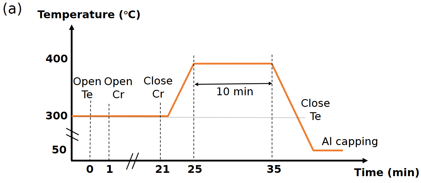
The Cr2Te3 films were grown using a two-step process as sketched in Fig. 1(a). The growth temperature, Te:Cr ratio and deposition rate were set at 300°C, 10, and 0.25 L/min respectively. The Te cell shutter was opened 1 minute before chromium deposition to ensure that the surface of the substrate was saturated in Te at the first stage of growth [see Fig. 1(a)]. After the growth, the samples were annealed at 400°C for 10 minutes using the same Te flux as during the growth and a heating ramp of 40°C/min. The samples were then cooled down to 50°C and 3 nm of aluminum was deposited to prevent oxidation of the layers during transfers between experimental setups.
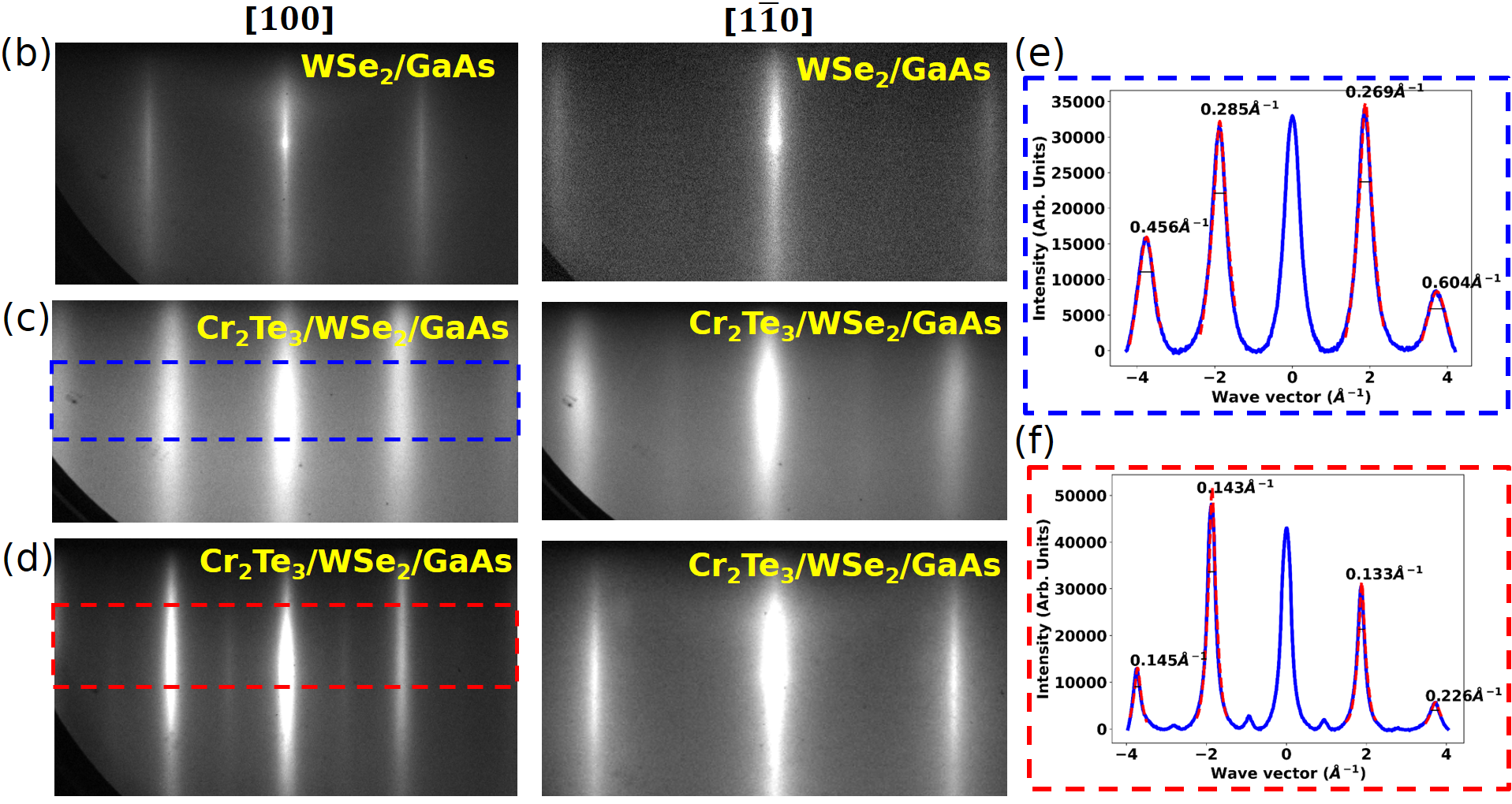
The film morphology was monitored in situ by reflection high-energy electron diffraction (RHEED) as can be seen in Fig. 1(b) in the case of WSe2. A streaky diffraction pattern was observed indicating a flat and well-crystallized surface. The different diffraction patterns along the two high symmetry axes of the WSe2 substrate [Fig. 1(c)-(e)] indicate a good alignment of Cr2Te3 grains with the underlying layer. After annealing, the width of the diffraction rods is approximately divided by 2 as a consequence of the larger grain size [Fig. 1(d)-(f)]. We made similar RHEED observations for the two other vdW substrates Bi2Te3 and graphene (see the Supplemental Material Fig. S1), except an increased isotropic contribution on graphene attributed to a lower interaction with the substrate.
IV Structural properties
We found similar structural characteristics for Cr2Te3 grown on WSe2 and graphene. Therefore, we present the results of the growth on WSe2 and the ones on graphene are given in the Supplemental Material. The results on Bi2Te3 are shown in Fig. 5.
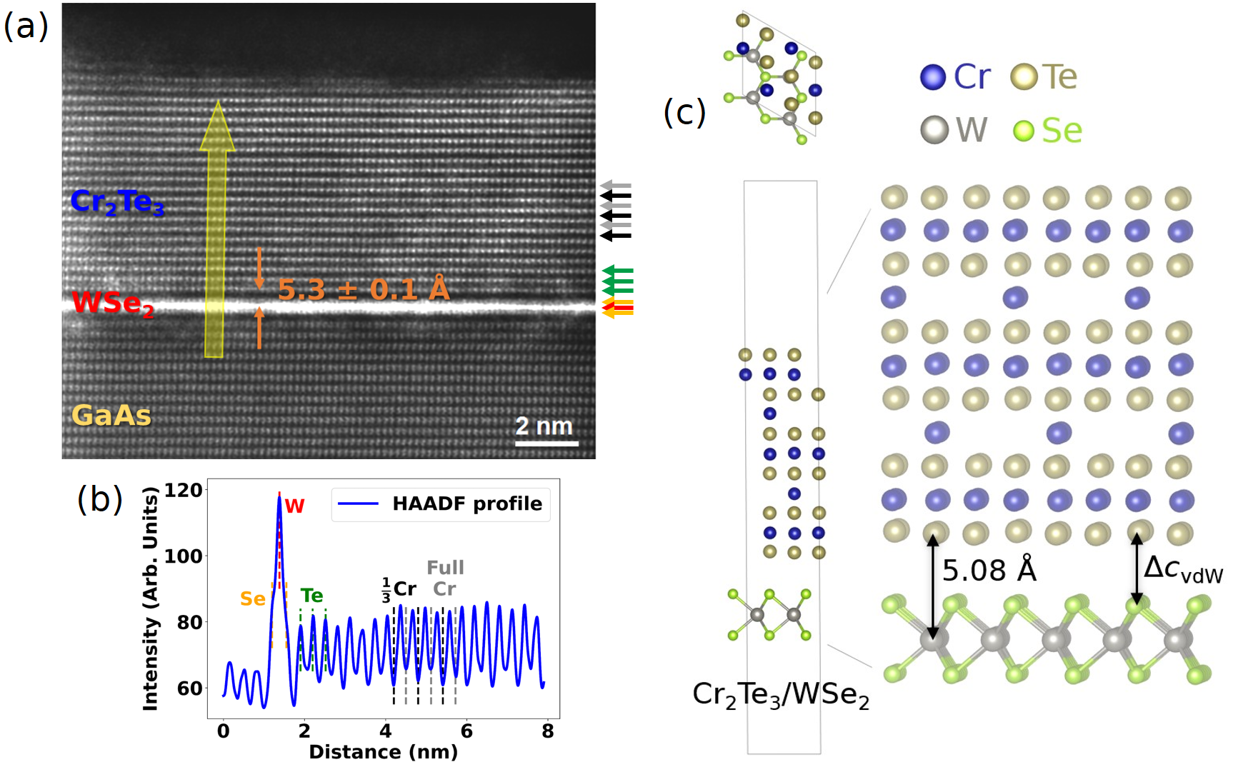
Figure 2(a) is a cross-section STEM image of the layers, revealing a sharp and well-defined interface between the vdW ferromagnet and the 2D layer as evidenced by the W-Te distance between W atoms of WSe2 and the first Te atoms plane of Cr2Te3 with a value of 5.3 Å. This value is taken to obtain a better experimental determination of the gap (due to the large atomic number of W with respect to Se) as can be seen in Fig. 2(b) showing a line profile along the c-direction of the heterostructure. This corresponds to a vdW gap of 3.5 Å if we assume a relaxed WSe2 layer, in agreement with our XRD data (see Fig. 3). It is worth noting that we resolve an intensity difference between fully and partially filled Cr planes. Indeed, every two Cr planes, only one third of the lattice sites are occupied by intercalated Cr atoms in the case of Cr2Te3. We also observe that the monolayer of WSe2 remains intact after the growth of Cr2Te3 on top.
The experimental W-Te distance was compared with the one obtained by ab initio calculations performed on Cr2Te3/WSe2 consisting of 1.5 unit cell thick Cr2Te3 on top of a single layer of WSe2 [see Fig. 2(c)]. The calculated distance is 5.08 Å, in good agreement with the experimental one of 5.3 Å.
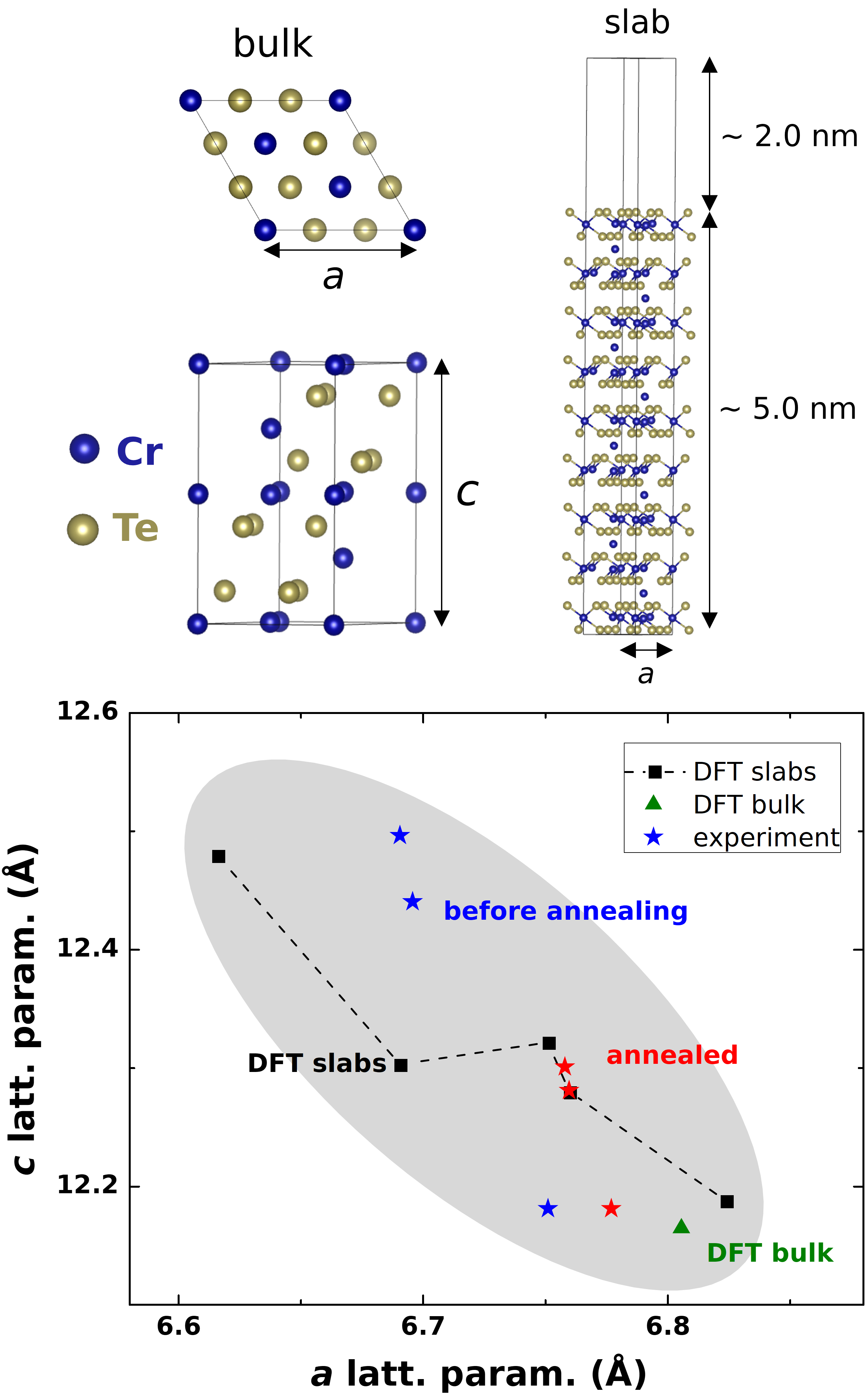
To accurately determine the lattice parameters of Cr2Te3 layers and crystal orientation with respect to each of the substrates, systematic XRD analysis were performed to extract the in-plane and out-of-plane lattice parameters. These measurements allowed us to measure accurately the strain in each layer when compared with the bulk lattice parameters.
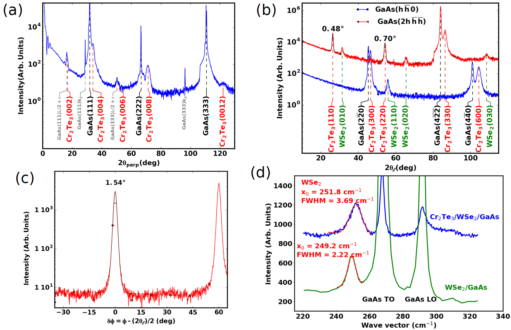
Figure 3(a), 3(b) and 3(c) show XRD out-of-plane, in-plane radial and in-plane azimuthal scans of Cr2Te3/WSe2/GaAs (sample 2, see Table 1) respectively. The diffraction patterns of Cr2Te3 deposited on WSe2 reveal the single crystalline character of the film and the clear epitaxial relationship with WSe2. The thin Bragg peaks in radial scans in Fig. 3(b) (Full Widths at Half Maximum -FWHM- of 0.48° and 0.70°) indicate the large grain size and the uniformity of the lattice parameter. In Fig. 3(c), the mosaic spread (FWHM of 1.54°) is negligibly small which confirms the perfect orientation of Cr2Te3 on WSe2 .
All the XRD data are summarized in Table 1. Compared to bulk values of Cr2Te3 with Å and Å [42], we systematically found an in-plane compressive strain and a resulting out-of-plane expansion. We found similar lattice parameters regardless of the substrate underneath although the mismatch between inter-atomic distances is very large (WSe2:+19.1%/Gr:+56.3%/Bi2Te3:-10.8%). An in-plane compressive strain would be expected for Cr2Te3 deposited on WSe2 and graphene, whereas an in-plane tensile strain would be expected for the growth on Bi2Te3. Moreover, we could not find any commensurable relationship between the in-plane lattice parameter of Cr2Te3 and the one of the substrate. This was confirmed by ab initio calculations: the lattice parameter of the vdW heterostructure corresponds to the one of bulk Cr2Te3 above 7 MLs of Cr2Te3, as demonstrated for Cr2Te3/Gr (see the Supplemental Material Fig. S2). We thus conclude about the pure vdW interaction between Cr2Te3 and the substrate. The slight difference between lattice parameters might be due to the surface topography (presence of steps, terrace, etc.) and the microscopic structure of Cr2Te3 (grain size, grain boundaries, etc.).
| N° | 2D layer | Temperature | a (Å) | c (Å) | Stoichiometry | |||||
|---|---|---|---|---|---|---|---|---|---|---|
| 1 | WSe2 | 300°C | 6.731 | -1.2% | 12.44 | +3.1% | 1.848 | 1.00° | 2.36° | |
| 2 | WSe2 | 400°C | 6.760 | -0.76% | 12.28 | +1.7% | 1.817 | 0.62° | 1.54° | |
| 3 | graphene | 300°C | 6.754 | -0.88% | 12.18 | +0.91% | 1.804 | 0.72° | 24.8° | Cr1.88Te3 |
| 4 | graphene | 400°C | 6.758 | -0.79% | 12.30 | +1.9% | 1.820 | 0.60° | 16.6° | |
| 5 | Bi2Te3 | 300°C | 6.691 | -1.8% | 12.50 | +3.6% | 1.868 | 0.87° | 2.77° | Cr1.97Te3 |
| 6 | Bi2Te3 | 400°C | 6.778 | -0.50% | 12.18 | +0.91% | 1.797 | 0.56° | 1.28° | Cr2.07Te3 |
However, the energy given to the system by annealing seems to be the driving force to control the final crystal structure since all the lattice parameters converge to the same values after annealing at 400°C. Besides, layers grown on graphene exhibit a much larger mosaic spread even after annealing, indicating even lower interaction between Cr2Te3 and the substrate during growth.
The measured lattice parameters match well with the ab initio calculations performed on nm-thick free-standing films which corresponds to the experimental thickness (see Fig. 4). In particular, for the Cr2Te3 films annealed on graphene and WSe2 (samples 2 and 4), the experimental lattice parameters fall exactly on the theoretical curve confirming a weak interaction between the film and the substrate. The case of Cr2Te3 grown on Bi2Te3 is discussed later in Fig. 5.
In Table 1, we also show the measured composition of some selected samples by RBS (see the Supplemental Material Fig. S4) and found compositions very close to Cr2Te3. No measurement could be performed on GaAs substrates as Ga and As are heavier than chromium, causing the Cr signal peak to lie in the substrate background, preventing any determination of the Cr:Te ratio in these samples.
Raman spectroscopy was also performed before and after the growth of Cr2Te3 to control the quality and integrity of the 2D layers. Figure 3(d) depicts the Raman spectra of WSe2/GaAs and Cr2Te3/WSe2/GaAs. The width and position of WSe2 peaks are preserved, indicating that the deposition of Cr2Te3 did not alter the WSe2 layer. The reference signal of WSe2/GaAs (green curve) was measured with a 532 nm laser instead of 633 nm as the other samples, explaining the intensity differences. Similar observations have been made on the Cr2Te3/graphene heterostructure as shown in the Supplemental Material Fig. S5.
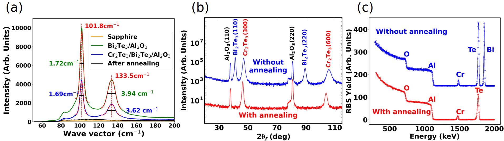
Figure 5(a) shows the Raman spectra of Cr2Te3/Bi2Te3/Al2O3 at different stages of growth. We detected two characteristic peaks of Bi2Te3 at 101.8 cm-1 and 133.5 cm-1, which correspond to the E and A vibrational modes and have also been reported in [43]. After the deposition of 5 layers of Cr2Te3 at 300°C, those peaks remained unchanged (the amplitude drop is explained by the partial absorption of the laser fluence in the metallic Cr2Te3 layer). However, when the sample was annealed at 400°C, the two characteristic peaks of Bi2Te3 disappeared. Indeed, x-ray diffraction measurements performed before and after annealing in Fig. 5(b) clearly show the disappearance of Bi2Te3 after thermal annealing. Finally, in Fig. 5(c), RBS measurements on the annealed sample show the absence of Bi in the heterostructure. This reveals that Bi2Te3 was evaporated during annealing leaving the Cr2Te3 film on the pristine sapphire substrate. We shaded the structural data of this sample (n°6) in Table 1 because Cr2Te3 is standing directly on the sapphire substrate after annealing. Moreover, in this case, the substrate is no more vdW and defects might have been created in Cr2Te3 by evaporation of the Bi2Te3 layer underneath.
V Magnetic properties
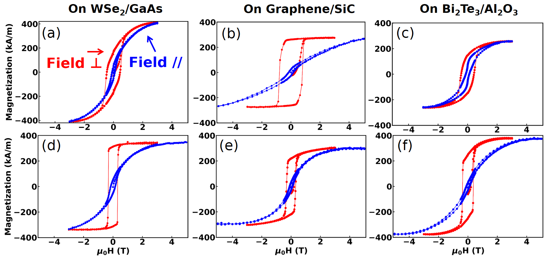
Hysteresis loops were measured by SQUID magnetometry at 5 K and are displayed in Fig. 6. For all samples, the easy axis of magnetization was found along the c-axis and by integrating the difference of area between the out-of-plane and the in-plane magnetization curves, the magnetic anisotropy energy (MAE) could be experimentally derived for all the samples.
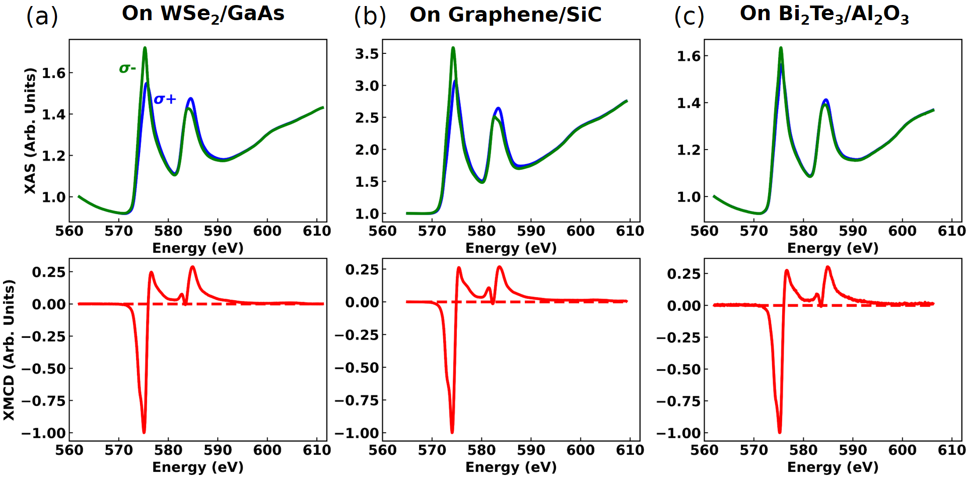
The origin of ferromagnetism in our layers was confirmed by XMCD performed at the SOLEIL synchrotron radiation source. The energy spectra are shown in Fig. 7 and a hysteresis loop is displayed in the Supplemental Material Fig. S6. A clear magnetic dichroism signal with a similar spectral shape was obtained for all the three different substrates. This proves that the chemical environment of Cr atoms in Cr2Te3 films is essentially independent of the substrate. The lower magnetic moment for the sample on Bi2Te3/Al2O3 [Fig. 7(c)] is explained by a lower sample thickness (three monolayers instead of five).
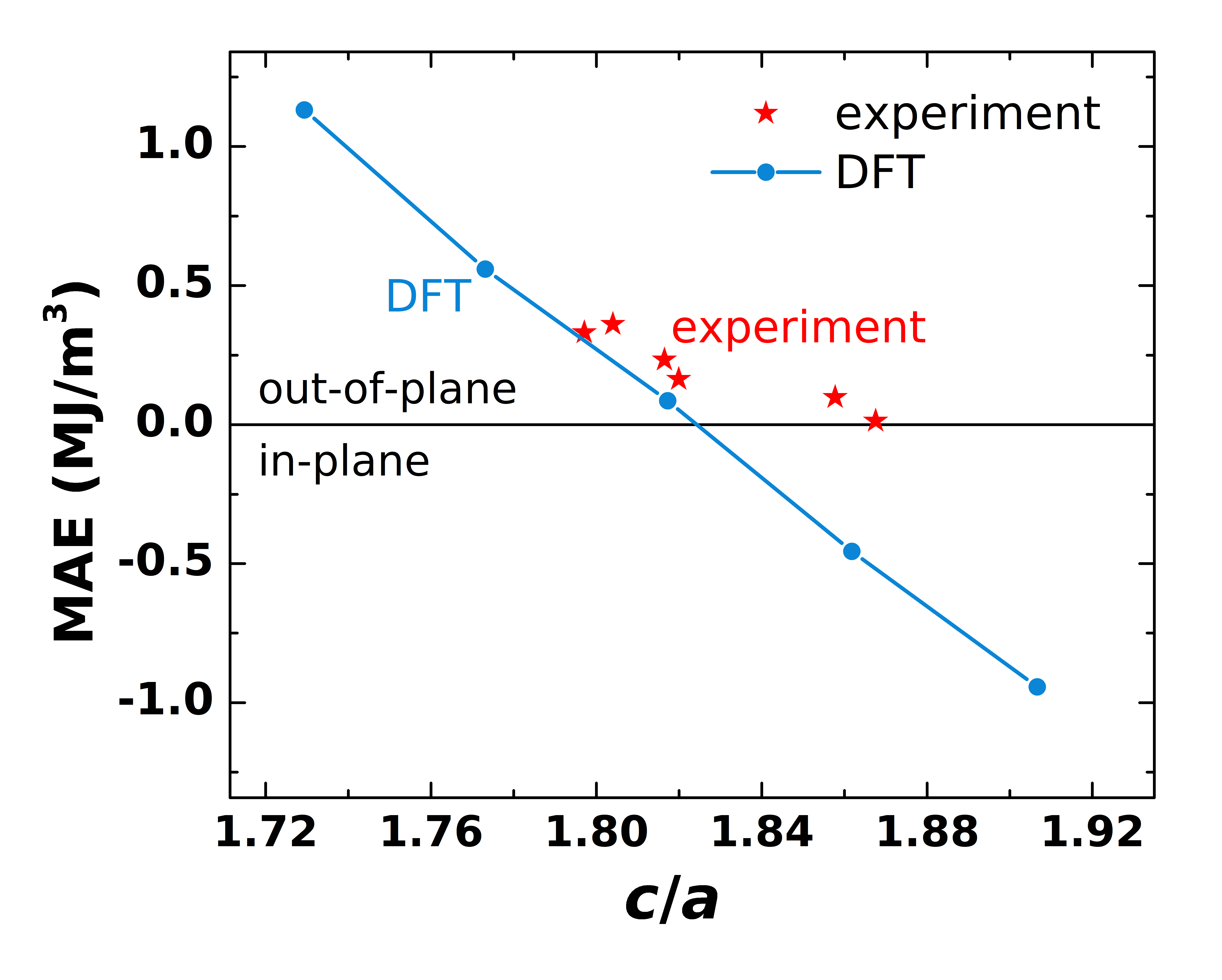
To better understand the magnetic properties, the magnetic anisotropy energy was calculated theoretically as a function of strain for bulk Cr2Te3 and was compared to experimental values in Fig. 8. The results reveal that the MAE is correlated to the strain of the layers. Overall, the trend and magnitude correspond well with experimental data. In particular, there is no sharp discontinuous change from positive to negative anisotropy values, as reported in [14]. However, the experimental data show larger PMA values compared to the theory. Since our calculations were performed in bulk Cr2Te3, we can attribute this shift to the presence of interfacial PMA at the Cr2Te3/substrate or Cr2Te3/AlOx capping layer interfaces.
To determine the of each annealed sample, we recorded the remanent magnetization after saturation at 5 T (with 5 K steps and no external field) as a function of temperature (Fig. 9). A value close to 180 K was found for the three substrates demonstrating again the very weak interaction between Cr2Te3 and the vdW substrates. Here, we believe that the is fully determined by the 2:3 stoichiometry of the films.

VI Magnetotransport
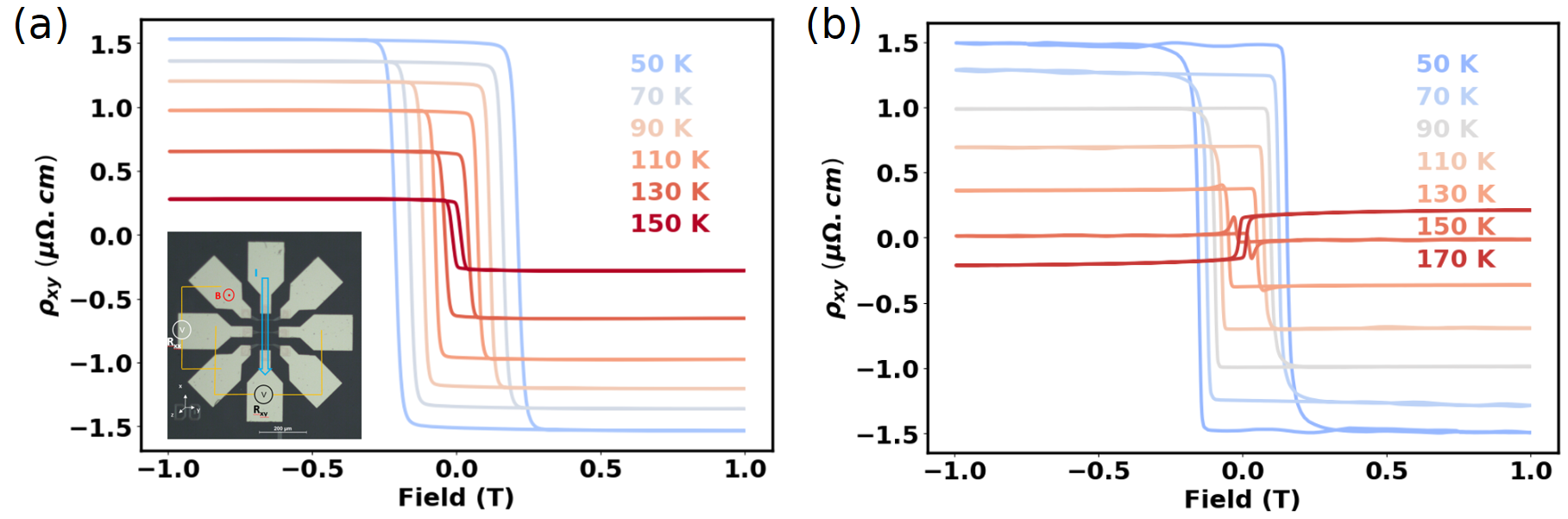
To study the magnetotransport properties, we performed four-probe resistance measurements and found an increasing longitudinal resistivity of Cr2Te3 layers with temperature indicating a metallic character (see the Supplemental Material Fig. S8). The resistivity is of the order of 500 .cm at 4 K. Figure 10(a) shows the Hall resistivity of 5 ML of Cr2Te3 deposited on WSe2 (sample 2) as a function of the perpendicular magnetic field at different temperatures. For visibility, the ordinary Hall slope was subtracted and a carrier density of 1.61015 holes/cm2 was extracted at 50 K, compared to 7.01015 holes/cm2 for 5 ML of Cr2Te3 directly deposited on sapphire (see the Supplemental Material Fig. S9), indicating a charge transfer from the WSe2 layer. The clear anomalous Hall signal confirmed the strong PMA of the ferromagnet.
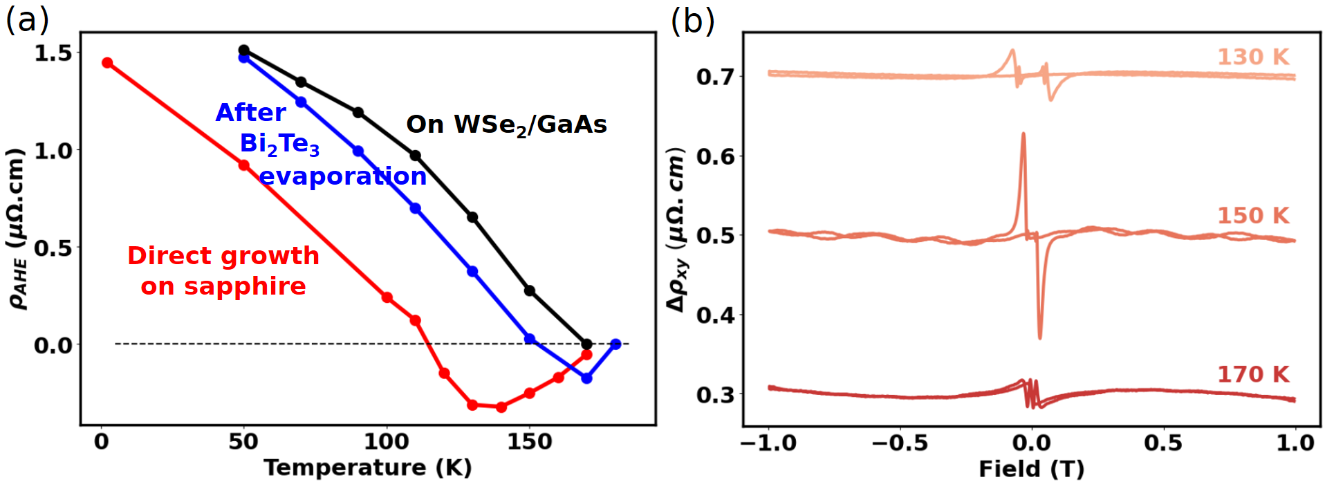
The same measurements were performed for a sample grown on Bi2Te3 (sample 6) and annealed at 400°C (resulting in Bi2Te3 evaporation), as shown in Fig. 10(b). The ordinary hall slope was removed and a carrier density of 4.51015 holes/cm2 was extracted at 50 K. Since there is no charge transfer with sapphire, the difference in carrier density with Cr2Te3 directly grown on sapphire could be explained by the presence of defects at the interface introduced during the evaporation of the Bi2Te3 layer.
In Fig. 11(a), the anomalous Hall resistivity is extracted for the two samples on sapphire as a function of temperature. We observe in both cases a sign change of the anomalous Hall resistivity below the Curie temperature of 180 K.
Similar observations were reported in [44, 45]. The possible origin of this effect is discussed in the following as a consequence of the energy-dependent Berry phase of Cr2Te3.
In the temperature range of the AH resistivity sign reversal, a resonance of the Hall signal manifested as peaks at the coercive fields can be observed. Figure 11(b) shows the Hall resistivity after subtraction of the ordinary and anomalous Hall effect at two temperatures below the sign change and one above. The bumps are enhanced when the temperature is closer (but still lower) than the temperature of the sign change and disappear above it. The width of the bumps also decreases with temperature, which could be related to the shrinking of the coercive field. The physical origin of such an effect is still under debate. In a similar heterostructure, Chen et al. [19] interpreted it as the topological Hall effect, which would originate from the presence of magnetic skyrmions. Skyrmions nucleate during the magnetization reversal and give rise to an extra transverse transport channel inducing a peak in the Hall resistivity. Imaging such spin textures has been performed by Lorentz-TEM in Cr3Te4 layers [46]. Nevertheless, another explanation has been put forward by other groups as two anomalous Hall contributions with opposite signs [47]. The origin could be thickness variations, inhomogeneities in the film or interface effects leading to the sign of the AHE being different [48, 49]. In the case of Cr2Te3 these peaks appear close to the anomalous Hall resistivity sign change. If the thickness of the layer is not strictly constant over the Hall bar, some areas could have slightly different temperatures at which the anomalous Hall signal changes sign. In this case, for intermediate temperatures, two AHE components with opposite signs would indeed add up and could explain the observed behavior.
The sign reversal of the anomalous Hall effect observed experimentally can be elucidated by ab initio calculations. The longitudinal resistivity is in the range where the contribution to AHE from intrinsic and impurity scattering components coexist, while the intrinsic part stays significant [45]. We thus calculated the intrinsic contribution to AHE for bulk Cr2Te3 (see Methods). As shown in Fig. 12, it exhibits a clear sign reversal very close to ( meV). This is in contrast with previous calculations [21] where the sign reversal occurs 330 meV above . This difference is due to the inclusion of the vdW corrections in our DFT calculations (see the Supplemental Material Fig. S10). We consider three different mechanisms influencing the value and sign of the anomalous Hall conductivity: (a) thermal broadening around the Fermi level (of the order of , i.e., 15 meV for K), (b) charge transfer with the substrate (which we calculated was greatest on graphene inducing a Fermi level shift of meV), and (c) out-of-plane strain (see the Supplemental Material Fig. S11). All these effects change the system energy in a range compatible with the calculations in Fig. 12.
We believe that the strain dependence of is at the origin of the change of sign of the AHE reported in Fig. 11(a). Anisotropic lattice expansion with temperature was reported for Cr1+δTe2 [50], which directly affects the AHE conductivity. To illustrate this qualitative argument, we chose in Fig. 12 two reasonable strain values in agreement with the structural data we obtained, keeping in mind that films in this work have ranging between 1.797 and 1.868 (see Fig. 8). If the Fermi level of the sample lies in the red shaded area (between -8 and 0 meV), the evolution of from 1.79 to 1.82 with temperature would lead to a sign change of .
Another effect that could influence this picture is the thermal broadening of the Fermi-Dirac distribution upon heating. However, we obtained a mostly linear dependence of on energy close to the Fermi level. When considering contributions above and below , both would cancel out as the thermal broadening is symmetric.
Finally, the role of the substrate has to be also accounted for. As shown experimentally, charge transfer with the 2D materials was observed and leads to a shift of the Fermi level. This explains why the effect is present for samples standing on sapphire and not for the one on WSe2. Indeed, for sapphire, the Fermi level is the lowest (carrier density of 4.51015 holes/cm2 and 7.01015 holes/cm2) so that we observe a sign change whereas the Fermi level is shifted up for WSe2 (1.61015 holes/cm2) and the sign change is absent. This observation is in agreement with the fact that the sign change in ab initio calculations occurs for lower energies as shown in Fig. 12.

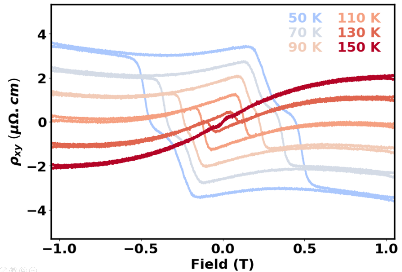
Finally, in Fig. 13, we present magnetotransport measurements on 5 layers of Cr2Te3 grown on graphene/SiC (sample 3). Both layers are metallic and contribute to conduction. The Hall resistivity is plotted as a function of the applied perpendicular magnetic field at different temperatures. No anomalous Hall resistivity sign change is measurable below the Curie temperature. This observation is in good agreement with ab initio calculations since the extracted carrier density at 50 K, which is the lowest: 1.41014 holes/cm2, corresponds to a Fermi level position shifted towards higher values. On top of the anomalous Hall contribution following the magnetization reversal at 0.5 T (at 50 K), another step close to 0.4 T is also present. This two-step signal behavior (absent in SQUID and XMCD measurements) vanishes progressively when increasing the temperature and disappears around 100 K, well below the Curie temperature. The origin of this effect needs further investigation and is out of the scope of the present work.
VII Conclusion
In conclusion, we reported the vdW epitaxy of Cr2Te3 on three different 2D materials. We revealed the pristine interface and the preservation of the intrinsic properties of the underlying layers after the growth of the vdW ferromagnet. We demonstrated the free-standing character of Cr2Te3 layers grown on these 2D materials after an annealing step at 400°C. Besides, the energy given to the system during the growth was identified as a way to control the crystal structure and tune the magnetic properties. We observed a correlation between the PMA energy of the system and the lattice parameters which was elucidated by ab initio calculations. Finally, we theoretically predicted a strain-sensitive sign change of the Berry phase very close to the Fermi level explaining the measured sign change of AHE with temperature. Charge transfer between the 2D layers and Cr2Te3 was shown to directly affect the temperature at which the AHE changes sign by shifting the Fermi level. To summarize, this system outputs highly tunable structural, magnetic and electrical properties, which presents an important asset for future spintronic applications.
Acknowledgments
This project has received funding from the European Union’s Horizon 2020 research and innovation programme under grant agreement No 800945 — NUMERICS — H2020-MSCA-COFUND-2017 and grant agreement 881603 (Graphene Flagship). We also acknowledge the French National Research Agency through the MAGICVALLEY project (ANR-18-CE24-0007) and the ESR-Equipex+ project 2D-MAG on two-dimensional magnetic materials. We acknowledge the financial support from the ANR project ELMAX (ANR-20-CE24-0015) and from the LANEF framework (ANR-10-LABX-51-01) for its support with mutualized infrastructure. This work was partly supported by the French RENATECH network. XMCD experiments were performed on the DEIMOS beamline at SOLEIL Synchrotron, France (proposal number 20220542). We are grateful to the SOLEIL staff for smoothly running the facility.
References
- Gong et al. [2017] C. Gong, L. Li, Z. Li, H. Ji, A. Stern, Y. Xia, T. Cao, W. Bao, C. Wang, Y. Wang, Z. Q. Qiu, R. J. Cava, S. G. Louie, J. Xia, and X. Zhang, Discovery of intrinsic ferromagnetism in two-dimensional van der Waals crystals, Nature 546, 265 (2017).
- Huang et al. [2017] B. Huang, G. Clark, E. Navarro-Moratalla, D. R. Klein, R. Cheng, K. L. Seyler, D. Zhong, E. Schmidgall, M. A. McGuire, D. H. Cobden, W. Yao, D. Xiao, P. Jarillo-Herrero, and X. Xu, Layer-dependent ferromagnetism in a van der Waals crystal down to the monolayer limit, Nature 546, 270 (2017).
- Wang et al. [2022] Q. H. Wang, A. Bedoya-Pinto, M. Blei, A. H. Dismukes, A. Hamo, S. Jenkins, M. Koperski, Y. Liu, Q.-C. Sun, E. J. Telford, H. H. Kim, M. Augustin, U. Vool, J.-X. Yin, L. H. Li, A. Falin, C. R. Dean, F. Casanova, R. F. L. Evans, M. Chshiev, A. Mishchenko, C. Petrovic, R. He, L. Zhao, A. W. Tsen, B. D. Gerardot, M. Brotons-Gisbert, Z. Guguchia, X. Roy, S. Tongay, Z. Wang, M. Z. Hasan, J. Wrachtrup, A. Yacoby, A. Fert, S. Parkin, K. S. Novoselov, P. Dai, L. Balicas, and E. J. G. Santos, The magnetic genome of two-dimensional van der waals materials, ACS Nano 16, 6960 (2022).
- C. Ferrari et al. [2015] A. C. Ferrari, F. Bonaccorso, V. Fal’ko, K. S. Novoselov, S. Roche, P. Bøggild, S. Borini, F. H. L. Koppens, V. Palermo, N. Pugno, J. A. Garrido, R. Sordan, A. Bianco, L. Ballerini, M. Prato, E. Lidorikis, J. Kivioja, C. Marinelli, T. Ryhänen, A. Morpurgo, J. N. Coleman, V. Nicolosi, L. Colombo, A. Fert, M. Garcia-Hernandez, A. Bachtold, G. F. Schneider, F. Guinea, C. Dekker, M. Barbone, Z. Sun, C. Galiotis, A. N. Grigorenko, G. Konstantatos, A. Kis, M. Katsnelson, L. Vandersypen, A. Loiseau, V. Morandi, D. Neumaier, E. Treossi, V. Pellegrini, M. Polini, A. Tredicucci, G. M. Williams, B. H. Hong, J.-H. Ahn, J. M. Kim, H. Zirath, B. J. v. Wees, H. v. d. Zant, L. Occhipinti, A. D. Matteo, I. A. Kinloch, T. Seyller, E. Quesnel, X. Feng, K. Teo, N. Rupesinghe, P. Hakonen, S. R. T. Neil, Q. Tannock, T. Löfwander, and J. Kinaret, Science and technology roadmap for graphene, related two-dimensional crystals, and hybrid systems, Nanoscale 7, 4598 (2015).
- Yang et al. [2022] H. Yang, S. O. Valenzuela, M. Chshiev, S. Couet, B. Dieny, B. Dlubak, A. Fert, K. Garello, M. Jamet, D.-E. Jeong, K. Lee, T. Lee, M.-B. Martin, G. S. Kar, P. Sénéor, H.-J. Shin, and S. Roche, Two-dimensional materials prospects for non-volatile spintronic memories, Nature 606, 663 (2022).
- Liu et al. [2020] C. Liu, H. Chen, S. Wang, Q. Liu, Y.-G. Jiang, D. W. Zhang, M. Liu, and P. Zhou, Two-dimensional materials for next-generation computing technologies, Nature Nanotechnology 15, 545 (2020).
- Dieny and Chshiev [2017] B. Dieny and M. Chshiev, Perpendicular magnetic anisotropy at transition metal/oxide interfaces and applications, Rev. Mod. Phys. 89, 025008 (2017).
- Ribeiro et al. [2022] M. Ribeiro, G. Gentile, A. Marty, D. Dosenovic, H. Okuno, C. Vergnaud, J.-F. Jacquot, D. Jalabert, D. Longo, P. Ohresser, A. Hallal, M. Chshiev, O. Boulle, F. Bonell, and M. Jamet, Large-scale epitaxy of two-dimensional van der Waals room-temperature ferromagnet Fe5GeTe2, npj 2D Materials and Applications 6, 1 (2022).
- Freitas et al. [2015] D. C. Freitas, R. Weht, A. Sulpice, G. Remenyi, P. Strobel, F. Gay, J. Marcus, and M. Núñez-Regueiro, Ferromagnetism in layered metastable 1 T -CrTe , Journal of Physics: Condensed Matter 27, 176002 (2015).
- Purbawati et al. [2020] A. Purbawati, J. Coraux, J. Vogel, A. Hadj-Azzem, N. Wu, N. Bendiab, D. Jegouso, J. Renard, L. Marty, V. Bouchiat, A. Sulpice, L. Aballe, M. Foerster, F. Genuzio, A. Locatelli, T. O. Menteş, Z. V. Han, X. Sun, M. Núñez-Regueiro, and N. Rougemaille, In-Plane Magnetic Domains and Néel-like Domain Walls in Thin Flakes of the Room Temperature CrTe2 Van der Waals Ferromagnet, ACS Applied Materials & Interfaces 12, 30702 (2020).
- Zhang et al. [2021] X. Zhang, Q. Lu, W. Liu, W. Niu, J. Sun, J. Cook, M. Vaninger, P. F. Miceli, D. J. Singh, S.-W. Lian, T.-R. Chang, X. He, J. Du, L. He, R. Zhang, G. Bian, and Y. Xu, Room-temperature intrinsic ferromagnetism in epitaxial CrTe2 ultrathin films, Nature Communications 12, 2492 (2021).
- Fujisawa et al. [2020] Y. Fujisawa, M. Pardo-Almanza, J. Garland, K. Yamagami, X. Zhu, X. Chen, K. Araki, T. Takeda, M. Kobayashi, Y. Takeda, C. H. Hsu, F. C. Chuang, R. Laskowski, K. H. Khoo, A. Soumyanarayanan, and Y. Okada, Tailoring magnetism in self-intercalated Cr1+xTe 2 epitaxial films, Physical Review Materials 4, 114001 (2020).
- Dijkstrat et al. [1989] J. Dijkstrat, H. H. Weitering’i, C. F. van Bruggen, C. Haast, and de Groot, Band-structurecalculations, and magnetic and transport properties of ferromagnetic chromium tellurides (CrTe, Cr3Te4,Cr,Te,), Journal of Physics: Condensed Matter 1, 9141 (1989).
- Wen et al. [2020] Y. Wen, Z. Liu, Y. Zhang, C. Xia, B. Zhai, X. Zhang, G. Zhai, C. Shen, P. He, R. Cheng, L. Yin, Y. Yao, M. Getaye Sendeku, Z. Wang, X. Ye, C. Liu, C. Jiang, C. Shan, Y. Long, and J. He, Tunable Room-Temperature Ferromagnetism in Two-Dimensional Cr Te , Nano Letters 20, 3130 (2020).
- Li et al. [2019] H. Li, L. Wang, J. Chen, T. Yu, L. Zhou, Y. Qiu, H. He, F. Ye, I. K. Sou, and G. Wang, Molecular Beam Epitaxy Grown Cr Te Thin Films with Tunable Curie Temperatures for Spintronic Devices, ACS Applied Nano Materials 2, 6809 (2019).
- Zhou et al. [2022] J. Zhou, X. Song, J. Chai, N. L. M. Wong, X. Xu, Y. Jiang, Y. P. Feng, M. Yang, and S. Wang, Structure dependent and strain tunable magnetic ordering in ultrathin chromium telluride, Journal of Alloys and Compounds 893, 162223 (2022).
- Li et al. [2021] Q.-Q. Li, S. Li, D. Wu, Z.-K. Ding, X.-H. Cao, L. Huang, H. Pan, B. Li, K.-Q. Chen, and X.-D. Duan, Magnetic properties manipulation of CrTe2 bilayer through strain and self-intercalation, Applied Physics Letters 119, 162402 (2021).
- Coughlin et al. [2021] A. L. Coughlin, D. Xie, X. Zhan, Y. Yao, L. Deng, H. Hewa-Walpitage, T. Bontke, C.-W. Chu, Y. Li, J. Wang, H. A. Fertig, and S. Zhang, Van der Waals Superstructure and Twisting in Self-Intercalated Magnet with Near Room-Temperature Perpendicular Ferromagnetism, Nano Letters 21, 9517 (2021).
- Chen et al. [2019] J. Chen, L. Wang, M. Zhang, L. Zhou, R. Zhang, L. Jin, X. Wang, H. Qin, Y. Qiu, J. Mei, F. Ye, B. Xi, H. He, B. Li, and G. Wang, Evidence for Magnetic Skyrmions at the Interface of Ferromagnet/Topological-Insulator Heterostructures, Nano Letters 19, 6144 (2019).
- Chen et al. [2022] J. Chen, L. Zhou, L. Wang, Z. Yan, X. Deng, J. Zhou, J.-w. Mei, Y. Qiu, B. Xi, X. Wang, H. He, and G. Wang, Conformal Growth of Cr Te on Bi Te Nanodots with a Topological Hall Effect, Crystal Growth & Design 22, 140 (2022).
- Jeon et al. [2022] J. H. Jeon, H. R. Na, H. Kim, S. Lee, S. Song, J. Kim, S. Park, J. Kim, H. Noh, G. Kim, S.-K. Jerng, and S.-H. Chun, Emergent Topological Hall Effect from Exchange Coupling in Ferromagnetic Cr2Te3/Noncoplanar Antiferromagnetic Cr2Se3 Bilayers, ACS Nano , 9 (2022).
- Pramanik et al. [2017] T. Pramanik, A. Roy, R. Dey, A. Rai, S. Guchhait, H. C. Movva, C.-C. Hsieh, and S. K. Banerjee, Angular dependence of magnetization reversal in epitaxial chromium telluride thin films with perpendicular magnetic anisotropy, Journal of Magnetism and Magnetic Materials 437, 72 (2017).
- Ueno et al. [1990] K. Ueno, K. Saiki, T. Shimada, and A. Koma, Epitaxial growth of transition metal dichalcogenides on cleaved faces of mica, Journal of Vacuum Science & Technology A 8, 68 (1990).
- Ohuchi et al. [1990] F. S. Ohuchi, B. A. Parkinson, K. Ueno, and A. Koma, van der Waals epitaxial growth and characterization of MoSe2 thin films on SnS2, Journal of Applied Physics 68, 2168 (1990).
- Dau et al. [2018] M. T. Dau, M. Gay, D. Di Felice, C. Vergnaud, A. Marty, C. Beigné, G. Renaud, O. Renault, P. Mallet, T. Le Quang, J.-Y. Veuillen, L. Huder, V. T. Renard, C. Chapelier, G. Zamborlini, M. Jugovac, V. Feyer, Y. J. Dappe, P. Pochet, and M. Jamet, Beyond van der Waals Interaction: The Case of MoSe2 Epitaxially Grown on Few-Layer Graphene, ACS Nano 12, 2319 (2018).
- Dappe et al. [2020] Y. J. Dappe, Y. Almadori, M. T. Dau, C. Vergnaud, M. Jamet, C. Paillet, T. Journot, B. Hyot, P. Pochet, and B. Grévin, Charge transfers and charged defects in WSe2/graphene-SiC interfaces, Nanotechnology 31, 255709 (2020).
- Ohresser et al. [2014] P. Ohresser, E. Otero, F. Choueikani, K. Chen, S. Stanescu, F. Deschamps, T. Moreno, F. Polack, B. Lagarde, J.-P. Daguerre, F. Marteau1, F. Scheurer, L. Joly, J.-P. Kappler, B. Muller, O. Bunau, and P. Sainctavit, Deimos: A beamline dedicated to dichroism measurements in the 350–2500 ev energy range, Review of Scientific Instruments 85, 013106 (2014).
- Kresse and Hafner [1993] G. Kresse and J. Hafner, Ab initio molecular dynamics for liquid metals, Physical Review B 47, 558 (1993).
- Kresse and Furthmüller [1996] G. Kresse and J. Furthmüller, Efficiency of ab-initio total energy calculations for metals and semiconductors using a plane-wave basis set, Computational Materials Science 6, 15 (1996).
- Perdew et al. [1996] J. P. Perdew, K. Burke, and M. Ernzerhof, Generalized Gradient Approximation Made Simple, Physical Review Letters 77, 3865 (1996).
- Dudarev et al. [1998] S. L. Dudarev, G. A. Botton, S. Y. Savrasov, C. J. Humphreys, and A. P. Sutton, Electron-energy-loss spectra and the structural stability of nickel oxide: An LSDA+U study, Physical Review B 57, 1505 (1998).
- Grimme et al. [2010] S. Grimme, J. Antony, S. Ehrlich, and H. Krieg, A consistent and accurate ab initio parametrization of density functional dispersion correction (DFT-D) for the 94 elements H-Pu, The Journal of Chemical Physics 132, 154104 (2010).
- Grimme et al. [2011] S. Grimme, S. Ehrlich, and L. Goerigk, Effect of the damping function in dispersion corrected density functional theory, Journal of Computational Chemistry 32, 1456 (2011).
- Choudhary et al. [2020] K. Choudhary, K. F. Garrity, S. T. Hartman, G. Pilania, and F. Tavazza, Efficient computational design of 2d van der waals heterostructures: Band-alignment, lattice-mismatch, web-app generation and machine-learning, arXiv: Materials Science (2020).
- Hallal et al. [2014] A. Hallal, B. Dieny, and M. Chshiev, Impurity-induced enhancement of perpendicular magnetic anisotropy in Fe/MgO tunnel junctions, Physical Review B 90, 064422 (2014).
- Wang et al. [2006] X. Wang, J. R. Yates, I. Souza, and D. Vanderbilt, Ab initio calculation of the anomalous Hall conductivity by Wannier interpolation, Physical Review B 74, 195118 (2006).
- Mostofi et al. [2014] A. A. Mostofi, J. R. Yates, G. Pizzi, Y.-S. Lee, I. Souza, D. Vanderbilt, and N. Marzari, An updated version of wannier90: A tool for obtaining maximally-localised Wannier functions, Computer Physics Communications 185, 2309 (2014).
- Tsirkin [2021] S. S. Tsirkin, High performance Wannier interpolation of Berry curvature and related quantities with WannierBerri code, npj Computational Materials 7, 33 (2021).
- Destraz et al. [2020] D. Destraz, L. Das, S. S. Tsirkin, Y. Xu, T. Neupert, J. Chang, A. Schilling, A. G. Grushin, J. Kohlbrecher, L. Keller, P. Puphal, E. Pomjakushina, and J. S. White, Magnetism and anomalous transport in the Weyl semimetal PrAlGe: possible route to axial gauge fields, npj Quantum Materials 5, 5 (2020).
- Kumar et al. [2016] B. Kumar, M. Baraket, M. Paillet, J.-R. Huntzinger, A. Tiberj, A. Jansen, L. Vila, M. Cubuku, C. Vergnaud, M. Jamet, G. Lapertot, D. Rouchon, A.-A. Zahab, J.-L. Sauvajol, L. Dubois, F. Lefloch, and F. Duclairoir, Growth protocols and characterization of epitaxial graphene on SiC elaborated in a graphite enclosure, Physica E: Low-dimensional Systems and Nanostructures 75, 7 (2016).
- Pierucci et al. [2022] D. Pierucci, A. Mahmoudi, M. Silly, F. Bisti, F. Oehler, G. Patriarche, F. Bonell, A. Marty, C. Vergnaud, M. Jamet, H. Boukari, E. Lhuillier, M. Pala, and A. Ouerghi, Evidence for highly p-type doping and type II band alignment in large scale monolayer WSe2/Se-terminated GaAs heterojunction grown by molecular beam epitaxy, Nanoscale 14, 5859 (2022).
- Andresen et al. [1970] A. F. Andresen, E. Zeppezauer, T. Boive, B. Nordström, and C. Brändén, Magnetic structure of Cr2Te3, Cr3Te4, and Cr5Te6, Acta Chem. Scand. 24, 3495 (1970).
- Wang et al. [2013] C. Wang, X. Zhu, L. Nilsson, J. Wen, G. Wang, X. Shan, Q. Zhang, S. Zhang, J. Jia, and Q. Xue, In situ Raman spectroscopy of topological insulator Bi2Te3 films with varying thickness, Nano Research 6, 688 (2013).
- Chi et al. [2022] H. Chi, Y. Ou, T. B. Eldred, W. Gao, S. Kwon, J. Murray, M. Dreyer, R. E. Butera, A. C. Foucher, H. Ambaye, J. Keum, A. T. Greenberg, Y. Liu, M. R. Neupane, G. J. de Coster, O. A. Vail, P. J. Taylor, P. A. Folkes, C. Rong, G. Yin, R. K. Lake, F. M. Ross, V. Lauter, D. Heiman, and J. S. Moodera, Strain-tunable berry curvature in quasi-two-dimensional chromium telluride, arXiv preprint arXiv:2207.02318 (2022).
- Fujisawa et al. [2022] Y. Fujisawa, M. Pardo-Almanza, C. H. Hsu, A. Mohamed, K. Yamagami, A. Krishnadas, F. C. Chuang, K. H. Khoo, J. Zang, A. Soumyanarayanan, and Y. Okada, Widely tunable berry curvature in the magnetic semimetal cr1+ dte2, arXiv preprint arXiv:2204.02518 (2022).
- Zhang et al. [2022] C. Zhang, C. Liu, J. Zhang, Y. Yuan, Y. Wen, Y. Li, D. Zheng, Q. Zhang, Z. Hou, G. Yin, K. Liu, Y. Peng, and X.-X. Zhang, Room-temperature magnetic skyrmions and large topological hall effect in chromium telluride engineered by self-intercalation, Advanced Materials , 2205967 (2022).
- Tai et al. [2022] L. Tai, B. Dai, J. Li, H. Huang, S. K. Chong, K. L. Wong, H. Zhang, P. Zhang, P. Deng, C. Eckberg, G. Qiu, H. He, D. Wu, S. Xu, A. Davydov, R. Wu, and K. L. Wang, Distinguishing the two-component anomalous hall effect from the topological hall effect, ACS Nano 16, 17336 (2022).
- Wang et al. [2020] L. Wang, Q. Feng, H. G. Lee, E. K. Ko, Q. Lu, and T. W. Noh, Controllable thickness inhomogeneity and berry curvature engineering of anomalous hall effect in srruo3 ultrathin films, Nano Letters 20, 2468 (2020).
- Kimbell et al. [2022] G. Kimbell, C. Kim, W. Wu, M. Cuoco, and J. W. A. Robinson, Challenges in identifying chiral spin textures via the topological Hall effect, Communications Materials 3, 1 (2022).
- Li et al. [2022] C. Li, K. Liu, D. Jiang, C. Jin, T. Pei, T. Wen, B. Yue, and Y. Wang, Diverse Thermal Expansion Behaviors in Ferromagnetic Cr1-dTe with NiAs-Type, Defective Structures, Inorganic Chemistry 61, 14641 (2022).