Observation of 2D Weyl Fermion States in Epitaxial Bismuthene
Abstract
A two-dimensional (2D) Weyl semimetal featuring a spin-polarized linear band dispersion and a nodal Fermi surface is a new topological phase of matter. It is a solid-state realization of Weyl fermions in an intrinsic 2D system. The nontrivial topology of 2D Weyl cones guarantees the existence of a new form of topologically protected boundary states, Fermi string edge states. In this work, we report the realization of a 2D Weyl semimetal in monolayer-thick epitaxial bismuthene grown on SnS(Se) substrate. The intrinsic band gap of bismuthene is eliminated by the space-inversion-symmetry-breaking substrate perturbations, resulting in a gapless spin-polarized Weyl band dispersion. The linear dispersion and spin polarization of the Weyl fermion states are observed in our spin and angle-resolved photoemission measurements. In addition, the scanning tunneling microscopy/spectroscopy reveals pronounced local density of states at the edge, suggesting the existence of Fermi string edge states. These results open the door for the experimental exploration of the exotic properties of Weyl fermion states in reduced dimensions.
I Introduction
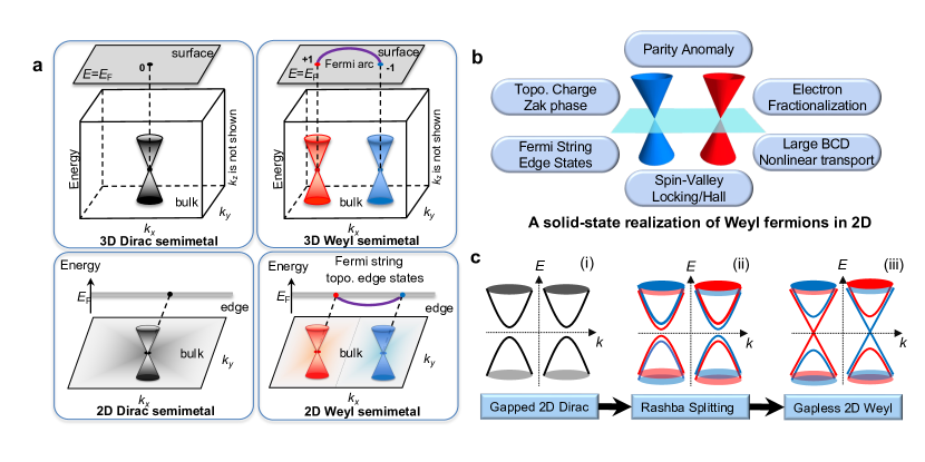
The discovery of Dirac materials, which feature massless states near the Fermi level, has driven the rise of the topological era in condensed matter physics. In particular, graphene, a two-dimensional (2D) Dirac semimetal, has enabled the exploration of relativistic physics in tabletop experiments[1, 2, 3]. The fundamental works on graphene set the foundation for future research ranging from topological insulators, valleytronics, to twistronics[4, 5, 6, 7, 8, 9]. The subsequent generalization from 2D to 3D platforms prompted the discovery of bulk Dirac semimetals. This generalization has shed light on the behaviors of higher dimensional massless carriers, tilted Dirac cones, and protected surface states[10, 11, 12, 13, 14, 15]. The discovery of Weyl semimetals, which host spin-split massless 3D quasiparticles, is particularly exciting since it is the first experimental realization of the Weyl fermion which was proposed long ago in the context of particle physics[16, 17, 18, 19, 15]. The chiral nodal points and 2D Fermi arc surface states of 3D Weyl semimetals bring about exotic properties such as chiral anomaly, unusual optical conductivity and nonlocal transport[20, 21, 22, 23, 24, 25, 26, 27, 28, 29, 30]. Generalization of a 3D Weyl fermion state to 2D gives a new topological state of matter, 2D Weyl semimetals that feature a spin-polarized linear band dispersion and a nodal Fermi surface. A simplistic illustration of Dirac and Weyl semimetals is presented in Fig. 1a highlighting the exotic states enabled by reducing the dimensionality from 3D to 2D.
The 2D Weyl semimetal state was discussed in Haldane’s seminal work as a critical phase in the model of quantum anomalous Hall effects [31]. The gapless linear dispersion without spin degeneracy establishes a solid-state realization of Weyl fermions in 2D space. The 2D Weyl fermion states, which correspond to linear bands around Weyl nodes at zero energy, are predicted to exhibit the parity anomaly in (2+1)-D (space–time) quantum field theory [32, 33, 34, 35] and electron fractionalization with zero modes of charge /2 [36]. The fractional zero modes are similar to those in the 1D systems by Jackiw and Rebbi [37] and by Su, Schrieffer and Hegger [38], and in -wave superconductors by Reed and Green [39]. The parity anomaly and charge fractionalization are only accessible in 2D Weyl semimetals rather than 2D Dirac semimetals for the quantum numbers would be “doubled” in spin degenerate states [36]. Despite the absence of a band gap, a 2D Weyl semimetal is characterized by a topological invariant, the winding number of the Weyl cone. The winding number can be obtained by integrating the Berry phase along a loop encircling each Weyl node,
| (1) |
where is the berry connection of the occupied valence bands [40]. The winding number of can be considered as the topological charge of 2D Weyl semimetals, which guarantees the existence of topologically protected edge states [41, 42]. These topological edge states take the form of Fermi strings (open strings) connecting the projection of bulk Weyl nodes at Fermi level in the edge Brillouin zone as shown Fig. 1a. The Fermi string edge states are the 1D analog of Fermi arc surface states in 3D Weyl semimetals. In this sense, 2D Weyl semimetals present a new example of bulk-boundary correspondence in a topological phase. Besides the exotic relativistic and topological properties, the spin and valley degrees of freedom are intrinsically entangled in 2D Weyl semimetals due to the spin polarization of massless electronic states. This unique spin-valley locking behavior of 2D Weyl semimetals gives rise to prominent spin Hall effects and valley Hall effects [43]. In addition, the spin-polarized Weyl cones cannot occur around time-reversal invariant momentum (TRIM) points in nonmagnetic 2D materials. Generally, the nodal points are located at generic points with reduced local symmetry, leading to a large asymmetry in the band dispersion. The asymmetric 2D Weyl cones give rise to a dramatic change of Berry curvature dipole (BCD) around the Fermi level, for the Berry curvature density diverges at the nodal point of linear bands [44, 45] (see Supplementary Information). Therefore, 2D Weyl semimetals provide an ideal platform for studying various nonlinear transport phenomena [44]. Those highly unusual properties (sketched in Fig. 1b) have inspired a myriad of recent theoretical works on 2D Weyl semimetals [46, 47, 42, 48, 49]. So far, however, experimental realization of topological 2D Weyl semimetals has remained elusive.
In this work, we report the discovery of a 2D Weyl semimetal in epitaxial bismuthene (a single atomic layer of bismuth stabilized in phosphorene structure[50, 51]). The 2D Weyl fermion states are achieved through an experimental procedure as shown in Fig. 1c. The first step is to find a 2D Dirac material with a narrow SOC gap such as silicene, antimonene, and bismuthene (Fig. 1ci)[52, 53, 54, 55, 56, 40]. After a suitable material is found, a perturbation is then applied to break space-inversion symmetry (Fig. 1cii). Such perturbations is commonly found in epitaxial films due to the electric potential from the substrate surface. Like a Rashba system, this perturbation induces spin splitting in the spin-degenerate bands and narrows down the band gap. The spin-split band structure is energetically favored compared to the spin-degenerate case since the energy gain in the down-moving occupied band is larger than the energy cost in the up-moving occupied bands (see Supplementary Information). In other words, the system tends to relax towards a configuration with a larger spin splitting and a narrower gap. With a sufficiently strong substrate perturbation, the band gap can be eliminated, resulting in a Weyl band structure (Fig. 1ciii). Using spin- and angle-resolved photoemission spectroscopy (spin-ARPES) and scanning tunneling spectroscopy (STS), we systematically study the electronic structure and spin texture of bismuthene (Bi monolayer in phosphorene structure) grown on SnS and SnSe substrates. The ARPES results demonstrate the spin-polarized gapless Weyl fermion states. Furthermore, the tunneling spectrum shows an enhanced local density of states at the edge of bismuthene, consistent with the calculated edge spectrum with Fermi string states. The experimental results unambiguously establish epitaxial bismuthene on SnS(Se) as an ideal 2D Weyl semimetal.
II The material base for hosting 2D Weyl fermion states
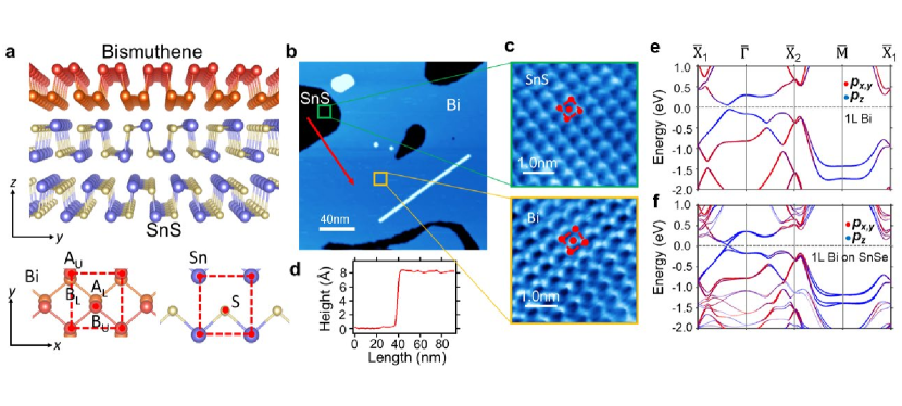
Bi, a group-Va pnictogen atom, typically forms three covalent bonds with its neighbors. In the 2D limit, two allotropic structural phases, the orthorhombic phosphorene-like phase [56] and the hexagonal honeycomb-like phase [57], are allowed by this requirement. The two phases are referred to as - and -phases, respectively, in the literature. Here we focus on the phosphorene-like -bismuthene (bismuthene for short in the following discussion). In our experiment, bismuthene thin films were grown with molecular beam epitaxy (MBE). The SnS(Se) was chosen as the substrate as it is van der Waals semiconductor and the (001) surface of SnS(Se) has a similar lattice structure as bismuthene. Figure 2a schematically shows the lattice structure of the sample. Bi atoms form a single-layer phosphorene structure on the (001) surface of SnS(Se). The Bi atoms have strong -hybridization character and thus the three BiBi bonds are close to a tetrahedral configuration. This leads to two atomic sublayers (marked with red and orange colours.) The lattice of bismuthene belongs to the space group (No. 53). The unit cell has a four-atom basis, which are labeled as A, A, B, and B (see the top view in Fig. 2a), where U and L refer to the upper and lower sublayer, respectively. The (001)-surface of SnS(Se) has a similar lattice as bismuthene but with S(Se) on A sites and Sn on B sites. The difference in electronegativity of Sn and S(Se) results in an in-plane dipole electric field, which causes an energy shift of A sites relative to B sites on average. In addition, the surface potential of SnS(Se) leads to an electric field perpendicular to the surface and causes a potential difference between the two Bi sublayers. Both the dipole field and the vertical field of the substrate surface break the space-inversion symmetry and give rise to spin splitting in the bands of bismuthene. We performed scanning-tunneling-microscope (STM) measurements to map the surface topography of the Bi sample grown on SnS(Se). The result is shown in Fig. 2b. The observed flat and uniform surface indicates the high structural quality of bismuthene. The red squares marked in the zoom-in STM images (Fig. 2c) demonstrate the surface unit cell of bismuthene and SnS. We found the in-plane lattice constants (, ) are (, ) for bismuthene, (, ) for SnS surface, and (, ) for SnSe surface, respectively. The apparent height of bismuthene (including the thickness of bimuthene and the spacing between bismuthene and SnS(001) surface) is 8.0Å, which can be seen from the height profile (Fig. 2d) taken along the red arrow marked in Fig. 2b.
III Band structure of the 2D Weyl semimetal
Here we present the first-principles band structures and angle-resolved photoemission spectroscopy (ARPES) spectra to demonstrate the existence of the 2D Weyl states in the epitaxial bismuthene films. The calculated band structure of free-standing bismuthene is shown in Fig. 2e. The only prominent band feature near the Fermi level is a gapped Dirac cone located at a generic point between and . The Dirac bands are dominated by orbitals of Bi atoms. The effective model around the Dirac point can be written as
| (2) |
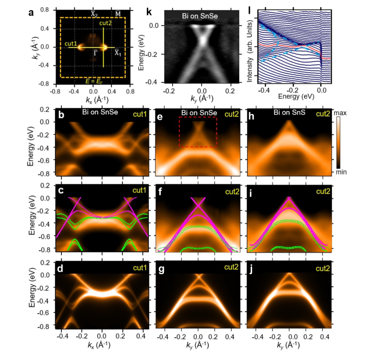
where (, ) are measured from the Dirac nodes at (, 0), (,,) are Pauli matrices with respect to the basis of (the orbitals on the two sublattices A and B), (,,) are the spin matrices, causes a tilting of the Weyl cone in direction and is crucial for generating a non-zero Berry curvature dipole (BCD) [44], is the effective spin-orbit coupling, represents the chirality of the Dirac nodes located at (, 0), and are Fermi velocity along and directions, respectively. m/s, m/s, m/s, meV according to the first-principles results. The energy gap induced by spin-orbit coupling is eV. Every band is doubly degenerate with respect to the spin degree of freedom since the lattice of bimuthene is centrosymmetric. The calculated band structure of bismuthene on SnSe is presented in Fig. 2f. The presence of SnSe substrate breaks space-inversion symmetry and causes spin splitting in the bands of bismuthene. Particularly, a linear band crossing formed in the same way as the 2D Weyl cone described in Fig. 1c. The states from SnSe can be found only below -0.9 eV and above 0.4 eV, because SnSe is a semiconductor with a gap of 1.3 eV. The 2D Weyl fermion states near the Fermi level are predominantly constructed by Bi orbitals and thus spatially confined in the epitaxial Bi layer, making the system an intrinsic 2D system.
With the inclusion of the substrate, the low-energy effective Hamiltonian is
| (3) | |||||
| (4) |
where describes the perturbation induced by the in-plane dipole field of the SnSe surface, and and are the Rashba couplings induced by the vertical electric field from the SnSe surface. The energy gap at the band crossing is
| (5) |
The quantity reflects the strength of substrate effects on the bands of bismuthene. The band gap vanishes when (see Supplementary Information). Remarkably, the gapless band dispersion is found in the first-principles band calculation. The calculated 2D Weyl band structure is confirmed by our ARPES measurements. The ARPES results taken from the bismuthene/SnSe sample are plotted in Fig. 3. The Fermi surface (Fig. 3a) contains two circular electron pockets in the direction of . We note that a similar pair of electron pockets shows up in the direction of but with much lower intensity. This extra pair of pockets is due to the existence of Bi domains rotated by in the MBE sample. The ARPES spectra for bismuthene on SnSe taken along the lines of “cut1” and “cut2” (marked in Fig. 3a) are plotted in Figs. 3b-g. In the ARPES spectra, we found the band dispersion along “cut1” (“cut2”) as well as that from a rotated Bi domain. This can be better seen in Figs. 3c,f with overlay of calculated bands on top of the ARPES spectra. The magenta lines are bands along “cut1” (“cut2”) while the green lines are bands along a direction perpendicular to “cut1” (“cut2”). Only the gapless Weyl cones stay close to the Fermi level, which means the transport and optical properties of this system are entirely determined by the low-energy Weyl fermion states. No apparent gap was found at the nodal point, as evidenced by the second derivative spectrum (Fig. 3k) and the map of energy distribution curves (Fig. 3l). We also notice that one linear band of Weyl cone is much dimmer than the other in the spectrum of “cut1”. This can be attributed to the photoemission matrix element effects. Figures 3d, g shows the calculated spectra with the inclusion of the photoemission matrix elements, which agrees well with the ARPES result. The bismuthene/SnSe sample is electron-doped as the nodal point lies 0.1 eV below the Fermi level. The shift of the Fermi level can be attributed to the electron transfer from the SnSe substrate to the epitaxial bismuthene. We also performed ARPES measurements on bismuthene grown on SnS, and the results are plotted in Figs. 3h-j. Compared with bismuthene/SnSe, the Fermi level of bimuthene/SnS is slightly lower (due to the difference in electronegativity of Sn and S) and lies right at the Weyl node. Therefore, bismuthene/SnS is a perfect 2D Weyl semimetal with charge neutrality. Considering the different surface conditions of SnSe and SnS, the observation of Weyl cones in both sample configurations indicate the robustness of the 2D Weyl fermion states against weak perturbations.
IV Spin texture of the 2D Weyl cone
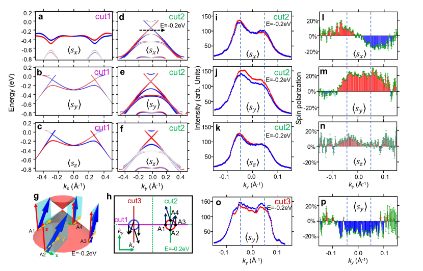
The defining character of Weyl fermion states is the spin polarization of the relativistic electronic states. According to Eq. 3, the dipole term () together with the SOC term cause the spin polarized in the direction while the vertical-field terms ( and ) give rise to an in-plane spin polarization (see the Supplementary Information for detailed discussions). As a result, a canted spin texture is expected for the Weyl cone. The two valleys of Weyl fermion states possess opposite spin polarizations because the two valleys are partners under the time-reversal symmetry. This is indeed what we found in the first-principles calculations and spin-resolved ARPES measurements as shown in Fig. 4. The calculated spin polarization of bands along “cut1” and “cut2” (marked in Fig. 4h) are shown in Figs. 4a-f. Along “cut1”, the Weyl bands near the fermi level carries nonzero and components. The absence of component is due to the fact that the direction corresponds to a glide line of the lattice (see Supplementary Information). By contrast, all three spin components show up in the bands along ”cut2”. The two linear bands of the Weyl cone in “cut2” have the same sign in the components but opposite signs in the component. The spin orientation of the states “A1”-“A4” at the lower Weyl cone is schematically plotted in Figs. 4g,h, which demonstrates the canted spin texture of the Weyl fermion states. To verify the spin texture of the Weyl fermion states, we performed spin-resolved ARPES measurements on bismuthene/SnSe. Spin-resolved momentum distribution curves (MDC) taken at eV below the Weyl node (along a line marked by the dashed arrow in Fig. 4d) are shown in Figs. 4i-k. The blue and red dotted lines are photoemission intensity recorded in the “spin-up” and “spin-down” channels for the corresponding spin component, respectively. The spin polarization (defined as , where the effective Sherman function = 0.275 for our spin detectors) is shown in Figs. 4l-n[58, 59]. The observed spin polarization of and is in good agreement with the theoretical results. The observed is less than the calculated value, which can be attributed to the existence of rotated Bi domains (see Supplementary Information). Nonetheless, the two branches of the Weyl cone have the same sign in the observed , which is consistent with the theoretical result in Fig. 4f. The measured spin polarization of states from the other valley along cut 3 shown in Figs. 4o,p provides a full view of the spin texture of the 2D Weyl semimetal. Our spin-ARPES results unambiguously confirm the canted spin texture and linear band dispersion of the Weyl cone in the epitaxial bismuthene.
V Bulk-boundary correspondence
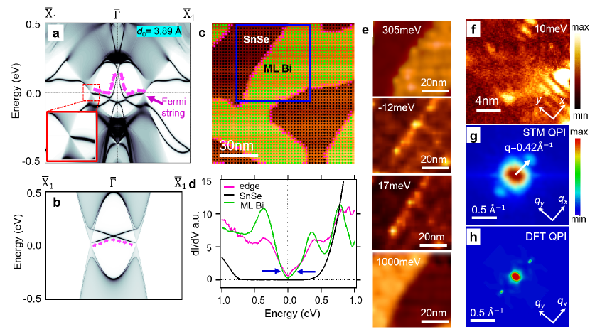
To show the unique bulk-boundary correspondence of 2D Weyl semimetals, we calculated the bands of a semi-infinite bismuthene/SnSe heterostructure with an open boundary in the (010) direction. The result is plotted in Fig. 5a. The Fermi string edge band directly connect the two bulk Weyl nodes as required by the band topology of the 2D Weyl cone. This Fermi string band is topologically protected and thus is robust against perturbations as shown in Supplementary Information. The connection of the ESBs to the bulk bands is schematically shown in Fig. 5b. Besides the Fermi string band, extra in-gap edge state bands exist between the two Weyl nodes. The existence of those extra edge state bands can be attributed to the fact that the 2D Weyl semimetal is at a critical point in connection to two topologically distinct insulator phases (see Supplementary Information for detailed discussion). The Fermi string edge band gives rise to an enhanced local density of states (LDOS) at the edge, especially, in a narrow energy window around the energy of bulk Weyl nodes. The LDOS can be directly probed by the differential conductivity dI/dV spectrum in scanning tunneling spectroscopy (STM) experiments. An STM topography of bismuthene on SnSe is shown in Fig. 5c. The surface of SnSe, the interior of bismuthene, and the edge of bismuthene are marked by the black, green, and magenta dots, respectively. We measured the averaged dI/dV spectrum at 4.6K from the three regions (black, green, and magenta), and the result is plotted in Fig. 5d. A large gap of1.3 eV is observed in SnSe, indicating the bulk Weyl states are entirely confined with the Bi overlayer. The spectral curve from the interior of bismuthene demonstrates a vanishing LDOS at the energy of Weyl nodes, , and linearity near , which is consistent with the linear band dispersion of Weyl cones. Remarkably, the edge dI/dV spectrum (magenta) shows a higher LDOS compared to the bulk spectrum (green) in a narrow energy window around marked by the two blue arrows. This enhanced LDOS can also be seen in the dI/dV maps taken near an edge (Fig. 5e). The edge is brighter than surfaces of SnSe and bismuthene at and 17 meV. A similar edge spectrum was observed in bismuthene/SnS samples (see Supplementary Information). The results are in accordance with the existence of topologically protected edge states near the Fermi level. Interestingly, the high-resolution dI/dV map reveals a unique plane wave-like pattern near the energy of Weyl nodes as shown in Fig. 5f. The Fourier transform of the dI/dV map gives the quasiparticle interference pattern (Fig. 5g), in which there is an oval contour at the center of the space accompanied by two small satellite contours. The distance between the satellite and the center of the oval is Å-1, which is exactly the separation between the two Weyl nodes in the 2D Brillouin as measured from ARPES results. Thus, the central oval contour in the QPI is from intravalley scatterings while the two satellites are induced by intervalley scatterings. The experimental QPI is consistent with the calculated result shown in Fig. 5h. The plane wave-like QPI with a single wavevector reflects the nodal Fermi surface of the 2D Weyl semimetal in epitaxial bismuthene.
VI Conclusion
The observation of gapless linear dispersion and spin texture of Weyl bands together with the enhanced edge density of states demonstrate epitaxial bismuthene/SnS(Se) as an ideal 2D Weyl semimetal with topological Fermi string edge states. This finding completes the family of solid-state Dirac and Weyl semimetals. The 2D Weyl semimetal in epitaxial bismuthene on SnS(Se) provides unique opportunities for exploring exotic relativistic and topological phenomena pertaining to Weyl fermions in 2D space.
VII Methods
VII.1 Growth of bismuthene on SnS and SnSe
Bi was deposited on the cleaved surface of SnS and SnSe crystals in an MBE-ARPES-STM ultrahigh vacuum (UHV) system. The SnS and SnSe crystals are n-type doped with Br. The base pressure was lower than mbar. High-purity Bi was evaporated from a standard Knudsen cell with a flux of 0.3 Å/min. The temperature of the substrate was kept at during the growth. The substrate temperature is critical for growing smooth Bi monolayer in the phosphorene structure.
VII.2 Scanning tunneling microscopy measurement
An in-situ Aarhus-150 STM was used to characterize the surface topography and the lattice parameters of the -Sb films. The topography was measured at room temperature with the base pressure lower than mbar. The bias voltage and the tunneling current were set to be 1.5 V and 0.01 nA for the surface topography measurement, 5 mV and 0.15 nA for the zoom-in atom-resolved STM measurement. The dI/dV spectrum, dI/dV mapping, and the STM QPI were produced by an Omicron LT-Nanoprobe system at 4.6K. The sample was transferred through a ultra-high vacuum (UHV) suitcase with pressure below mbar. The tunneling current is set to be 200 pA during the dI/dV measurement.
VII.3 Spin- and Angle-resolved photoemission spectroscopy measurements
Spin and angle resolved photoemission spectroscopy measurements were performed in a lab-based system coupled to the molecular beam epitaxy system, using a Scienta DA30L hemispherical analyzer with a base pressure of 510-11 mbar and a base temperature of 8 K. Samples were illuminated with linearly polarized light using an Oxide 11 eV laser system. The light polarization was set perpendicular to both the sample and the slits of the detector. For electronic dispersion measurements, a pass energy of 2 eV and 0.3 mm slit was used for a total energy resolution 2.5 meV and momentum resolution 0.01 . Dual VLEED ferrums that utilize exchange scattering are coupled to the electron analyzer and used to determine the spin , , and polarizations of the measured electrons. For spin resolved measurements a pass energy of 10 eV and a 1 mm 2 mm spin aperture was used yielding a total energy resolution 50 meV and momentum resolution 0.033 .
VII.4 First-principles calculation
First-principles calculations with Density Function Theory (DFT) were performed by using the Vienna ab Initio Simulation Package (VASP) package [60]. The Perdew-Burke-Ernzerhof (PBE) [61] exchange-correlation functional was used. The experimental lattice parameter was applied for bismuthene; the lattice parameter of SnSe(S) was modified to match the covered Bi. The spin-orbit coupling (SOC) was included self-consistently in the calculations of electronic structures with a Monkhorst-Pack 11111 -point mesh. The vacuum thickness was greater than 20 Å to ensure the separation of the slabs. Atomic relaxation was used until the residual forces were less than 0.01 eV/Å.
We constructed a tight-binding Hamiltonian for Bi/SnSe(S), where the tight-binding model matrix elements were calculated by projecting onto the Wannier orbitals[62, 63, 64], which used the VASP2WANNIER90 interface. The Bi orbitals, Sn orbitals, and Se orbitals were used to construct the Wannier functions without performing the maximizing localization. The edge state electronic structure was calculated by the Green’s function technique, which computes the spectral weight near the edge of a semi-infinite system. To simulate the photoemission matrix element effects in the ARPES spectra, we consider a non-trivial structure factor in ab initio calculations [65, 66]. To simulate this effect, we construct a unitary matrix :
where k is the momentum vector, is the real space coordinates of th atom in the original Bi/SnSe(S) unit cell. We simulate the unfolding band structures of Bi/SnSe via applying this unitary matrix to the tight-binding Hamiltonian, .
The quasiparticle interference pattern was calculated based on the Green’s function method by using spin-dependent scattering probability (SSP) method [67, 68], which can be written as
where is the total spectral density and is the spin density, in which is Green’s function of the system and are the Pauli matrices for spin.
References
- [1] K. S. Novoselov, A. K. Geim, S. V. Morozov, D. Jiang, M. I. Katsnelson, I. V. Grigorieva, S. V. Dubonos, and A. A. Firsov, “Two-dimensional gas of massless Dirac fermions in graphene,” Nature, vol. 438, no. 7065, pp. 197–200, 2005.
- [2] Y. Zhang, Y.-W. Tan, H. L. Stormer, and P. Kim, “Experimental observation of the quantum Hall effect and Berry’s phase in graphene,” Nature, vol. 438, no. 7065, pp. 201–204, 2005.
- [3] A. H. Castro Neto, F. Guinea, N. M. R. Peres, K. S. Novoselov, and A. K. Geim, “The electronic properties of graphene,” Reviews of Modern Physics, vol. 81, no. 1, pp. 109–162, 2009.
- [4] M. Z. Hasan and C. L. Kane, “Colloquium : Topological insulators,” Rev. Mod. Phys., vol. 82, pp. 3045–3067, Nov 2010.
- [5] X.-L. Qi and S.-C. Zhang, “Topological insulators and superconductors,” Rev. Mod. Phys., vol. 83, pp. 1057–1110, Oct 2011.
- [6] J. Li, R.-X. Zhang, Z. Yin, J. Zhang, K. Watanabe, T. Taniguchi, C. Liu, and J. Zhu, “A valley valve and electron beam splitter,” Science, vol. 362, no. 6419, pp. 1149–1152, 2018.
- [7] R. Ribeiro-Palau, C. Zhang, K. Watanabe, T. Taniguchi, J. Hone, and C. R. Dean, “Twistable electronics with dynamically rotatable heterostructures,” Science, vol. 361, no. 6403, pp. 690–693, 2018.
- [8] Y. Cao, V. Fatemi, A. Demir, S. Fang, S. L. Tomarken, J. Y. Luo, J. D. Sanchez-Yamagishi, K. Watanabe, T. Taniguchi, E. Kaxiras, R. C. Ashoori, and P. Jarillo-Herrero, “Correlated insulator behaviour at half-filling in magic-angle graphene superlattices,” Nature, vol. 556, no. 7699, pp. 80–84, 2018.
- [9] Y. Cao, V. Fatemi, S. Fang, K. Watanabe, T. Taniguchi, E. Kaxiras, and P. Jarillo-Herrero, “Unconventional superconductivity in magic-angle graphene superlattices,” Nature, vol. 556, no. 7699, pp. 43–50, 2018.
- [10] Z. K. Liu, B. Zhou, Y. Zhang, Z. J. Wang, H. M. Weng, D. Prabhakaran, S.-K. Mo, Z. X. Shen, Z. Fang, X. Dai, Z. Hussain, and Y. L. Chen, “Discovery of a Three-Dimensional Topological Dirac Semimetal, Na3Bi,” Science, vol. 343, no. 6173, pp. 864–867, 2014.
- [11] S.-Y. Xu, C. Liu, S. K. Kushwaha, R. Sankar, J. W. Krizan, I. Belopolski, M. Neupane, G. Bian, N. Alidoust, T.-R. Chang, H.-T. Jeng, C.-Y. Huang, W.-F. Tsai, H. Lin, P. P. Shibayev, F.-C. Chou, R. J. Cava, and M. Z. Hasan, “Observation of fermi arc surface states in a topological metal,” Science, vol. 347, no. 6219, pp. 294–298, 2015.
- [12] S. Borisenko, Q. Gibson, D. Evtushinsky, V. Zabolotnyy, B. Büchner, and R. J. Cava, “Experimental realization of a three-dimensional dirac semimetal,” Phys. Rev. Lett., vol. 113, p. 027603, Jul 2014.
- [13] M. Yan, H. Huang, K. Zhang, E. Wang, W. Yao, K. Deng, G. Wan, H. Zhang, M. Arita, H. Yang, Z. Sun, H. Yao, Y. Wu, S. Fan, W. Duan, and S. Zhou, “Lorentz-violating type-II Dirac fermions in transition metal dichalcogenide PtTe2,” Nature Communications, vol. 8, no. 1, p. 257, 2017.
- [14] J. Xiong, S. K. Kushwaha, T. Liang, J. W. Krizan, M. Hirschberger, W. Wang, R. J. Cava, and N. P. Ong, “Evidence for the chiral anomaly in the dirac semimetal na¡sub¿3¡/sub¿bi,” Science, vol. 350, no. 6259, pp. 413–416, 2015.
- [15] N. P. Armitage, E. J. Mele, and A. Vishwanath, “Weyl and dirac semimetals in three-dimensional solids,” Rev. Mod. Phys., vol. 90, p. 015001, Jan 2018.
- [16] X. Wan, A. M. Turner, A. Vishwanath, and S. Y. Savrasov, “Topological semimetal and fermi-arc surface states in the electronic structure of pyrochlore iridates,” Phys. Rev. B, vol. 83, p. 205101, May 2011.
- [17] S.-Y. Xu, I. Belopolski, N. Alidoust, M. Neupane, G. Bian, C. Zhang, R. Sankar, G. Chang, Z. Yuan, C.-C. Lee, S.-M. Huang, H. Zheng, J. Ma, D. S. Sanchez, B. Wang, A. Bansil, F. Chou, P. P. Shibayev, H. Lin, S. Jia, and M. Z. Hasan, “Discovery of a weyl fermion semimetal and topological fermi arcs,” Science, vol. 349, no. 6248, pp. 613–617, 2015.
- [18] B. Q. Lv, H. M. Weng, B. B. Fu, X. P. Wang, H. Miao, J. Ma, P. Richard, X. C. Huang, L. X. Zhao, G. F. Chen, Z. Fang, X. Dai, T. Qian, and H. Ding, “Experimental discovery of weyl semimetal taas,” Phys. Rev. X, vol. 5, p. 031013, Jul 2015.
- [19] A. A. Soluyanov, D. Gresch, Z. Wang, Q. Wu, M. Troyer, X. Dai, and B. A. Bernevig, “Type-II Weyl semimetals.,” Nature, vol. 527, no. 7579, pp. 495–8, 2015.
- [20] D. T. Son and B. Z. Spivak, “Chiral anomaly and classical negative magnetoresistance of weyl metals,” Phys. Rev. B, vol. 88, p. 104412, Sep 2013.
- [21] X. Huang, L. Zhao, Y. Long, P. Wang, D. Chen, Z. Yang, H. Liang, M. Xue, H. Weng, Z. Fang, X. Dai, and G. Chen, “Observation of the chiral-anomaly-induced negative magnetoresistance in 3d weyl semimetal taas,” Phys. Rev. X, vol. 5, p. 031023, Aug 2015.
- [22] C.-L. Zhang, S.-Y. Xu, I. Belopolski, Z. Yuan, Z. Lin, B. Tong, G. Bian, N. Alidoust, C.-C. Lee, S.-M. Huang, T.-R. Chang, G. Chang, C.-H. Hsu, H.-T. Jeng, M. Neupane, D. Sanchez, H. Zheng, J. Wang, H. Lin, C. Zhang, H.-Z. Lu, S.-Q. Shen, T. Neupert, M. Hasan, and S. Jia, “Signatures of the Adler-Bell-Jackiw chiral anomaly in a Weyl fermion semimetal,” Nature Communications, vol. 7, 2016.
- [23] C.-X. Liu, P. Ye, and X.-L. Qi, “Chiral gauge field and axial anomaly in a weyl semimetal,” Phys. Rev. B, vol. 87, p. 235306, Jun 2013.
- [24] H. Wei, S.-P. Chao, and V. Aji, “Excitonic phases from weyl semimetals,” Phys. Rev. Lett., vol. 109, p. 196403, Nov 2012.
- [25] P. E. C. Ashby and J. P. Carbotte, “Magneto-optical conductivity of weyl semimetals,” Phys. Rev. B, vol. 87, p. 245131, Jun 2013.
- [26] S. Jia, S.-Y. Xu, and M. Z. Hasan, “Weyl semimetals, Fermi arcs and chiral anomalies,” Nature Materials, vol. 15, no. 11, pp. 1140–1144, 2016.
- [27] A. A. Zyuzin and A. A. Burkov, “Topological response in weyl semimetals and the chiral anomaly,” Phys. Rev. B, vol. 86, p. 115133, Sep 2012.
- [28] S. A. Parameswaran, T. Grover, D. A. Abanin, D. A. Pesin, and A. Vishwanath, “Probing the chiral anomaly with nonlocal transport in three-dimensional topological semimetals,” Phys. Rev. X, vol. 4, p. 031035, Sep 2014.
- [29] E. V. Gorbar, V. A. Miransky, I. A. Shovkovy, and P. O. Sukhachov, “Nonlocal transport in weyl semimetals in the hydrodynamic regime,” Phys. Rev. B, vol. 98, p. 035121, Jul 2018.
- [30] M. Z. Hasan, G. Chang, I. Belopolski, G. Bian, S.-Y. Xu, and J.-X. Yin, “Weyl, Dirac and high-fold chiral fermions in topological quantum materials,” Nature Reviews Materials, vol. 0123456789, 2021.
- [31] F. D. M. Haldane, “Model for a quantum hall effect without landau levels: Condensed-matter realization of the ”parity anomaly”,” Phys. Rev. Lett., vol. 61, pp. 2015–2018, Oct 1988.
- [32] R. Jackiw, “Fractional charge and zero modes for planar systems in a magnetic field,” Phys. Rev. D, vol. 29, pp. 2375–2377, May 1984.
- [33] E. Fradkin, E. Dagotto, and D. Boyanovsky, “Physical realization of the parity anomaly in condensed matter physics,” Phys. Rev. Lett., vol. 57, pp. 2967–2970, Dec 1986.
- [34] G. W. Semenoff, “Condensed-matter simulation of a three-dimensional anomaly,” Phys. Rev. Lett., vol. 53, pp. 2449–2452, Dec 1984.
- [35] M. Mogi, Y. Okamura, M. Kawamura, R. Yoshimi, K. Yasuda, A. Tsukazaki, K. S. Takahashi, T. Morimoto, N. Nagaosa, M. Kawasaki, Y. Takahashi, and Y. Tokura, “Experimental signature of the parity anomaly in a semi-magnetic topological insulator,” Nature Physics, vol. 18, no. 4, pp. 390–394, 2022.
- [36] C.-Y. Hou, C. Chamon, and C. Mudry, “Electron fractionalization in two-dimensional graphenelike structures,” Phys. Rev. Lett., vol. 98, p. 186809, May 2007.
- [37] R. Jackiw and C. Rebbi, “Solitons with fermion number ½,” Phys. Rev. D, vol. 13, pp. 3398–3409, Jun 1976.
- [38] W. P. Su, J. R. Schrieffer, and A. J. Heeger, “Solitons in polyacetylene,” Phys. Rev. Lett., vol. 42, pp. 1698–1701, Jun 1979.
- [39] N. Read and D. Green, “Paired states of fermions in two dimensions with breaking of parity and time-reversal symmetries and the fractional quantum hall effect,” Phys. Rev. B, vol. 61, pp. 10267–10297, Apr 2000.
- [40] Y. Lu, D. Zhou, G. Chang, S. Guan, W. Chen, Y. Jiang, J. Jiang, X.-s. Wang, S. A. Yang, Y. P. Feng, Y. Kawazoe, and H. Lin, “Multiple unpinned Dirac points in group-Va single-layers with phosphorene structure,” npj Computational Materials, vol. 2, no. 1, p. 16011, 2016.
- [41] G. Bian, T.-R. Chang, R. Sankar, S.-Y. Xu, H. Zheng, T. Neupert, C.-K. Chiu, S.-M. Huang, G. Chang, I. Belopolski, D. S. Sanchez, M. Neupane, N. Alidoust, C. Liu, B. Wang, C.-C. Lee, H.-T. Jeng, C. Zhang, Z. Yuan, S. Jia, A. Bansil, F. Chou, H. Lin, and M. Z. Hasan, “Topological nodal-line fermions in spin-orbit metal PbTaSe2,” Nature Communications, vol. 7, no. 1, p. 10556, 2016.
- [42] J. D. Mella and L. E. F. F. Torres, “Robustness of spin-polarized edge states in a two-dimensional topological semimetal without inversion symmetry,” Phys. Rev. B, vol. 105, p. 075403, Feb 2022.
- [43] W.-F. Tsai, C.-Y. Huang, T.-R. Chang, H. Lin, H.-T. Jeng, and A. Bansil, “Gated silicene as a tunable source of nearly 100electrons,” Nature Communications, vol. 4, no. 1, p. 1500, 2013.
- [44] I. Sodemann and L. Fu, “Quantum nonlinear hall effect induced by berry curvature dipole in time-reversal invariant materials,” Phys. Rev. Lett., vol. 115, p. 216806, Nov 2015.
- [45] Z. Z. Du, H.-Z. Lu, and X. C. Xie, “Nonlinear Hall effects,” Nature Reviews Physics, vol. 3, no. 11, pp. 744–752, 2021.
- [46] X. Zhao, F. Ma, P.-J. Guo, and Z.-Y. Lu, “Two-dimensional quadratic double weyl semimetal,” Phys. Rev. Res., vol. 4, p. 043183, Dec 2022.
- [47] A. Panigrahi, V. Juričić, and B. Roy, “Projected topological branes,” Communications Physics, vol. 5, no. 1, p. 230, 2022.
- [48] Z.-R. Liu, L.-H. Hu, C.-Z. Chen, B. Zhou, and D.-H. Xu, “Topological excitonic corner states and nodal phase in bilayer quantum spin hall insulators,” Phys. Rev. B, vol. 103, p. L201115, May 2021.
- [49] H. Huan, Y. Xue, B. Zhao, H. Bao, L. Liu, and Z. Yang, “Tunable weyl half-semimetals in two-dimensional iron-based materials ,” Phys. Rev. B, vol. 106, p. 125404, Sep 2022.
- [50] H. Liu, A. T. Neal, Z. Zhu, Z. Luo, X. Xu, D. Tománek, and P. D. Ye, “Phosphorene: An Unexplored 2D Semiconductor with a High Hole Mobility,” ACS Nano, vol. 8, pp. 4033–4041, apr 2014.
- [51] L. Li, Y. Yu, G. J. Ye, Q. Ge, X. Ou, H. Wu, D. Feng, X. H. Chen, and Y. Zhang, “Black phosphorus field-effect transistors,” Nat Nano, vol. 9, pp. 372–377, may 2014.
- [52] C.-C. Liu, W. Feng, and Y. Yao, “Quantum spin hall effect in silicene and two-dimensional germanium,” Phys. Rev. Lett., vol. 107, p. 076802, Aug 2011.
- [53] L. Chen, C.-C. Liu, B. Feng, X. He, P. Cheng, Z. Ding, S. Meng, Y. Yao, and K. Wu, “Evidence for dirac fermions in a honeycomb lattice based on silicon,” Phys. Rev. Lett., vol. 109, p. 056804, Aug 2012.
- [54] Q. Lu, J. Cook, X. Zhang, K. Y. Chen, M. Snyder, D. T. Nguyen, P. V. S. Reddy, B. Qin, S. Zhan, L.-D. Zhao, P. J. Kowalczyk, S. A. Brown, T.-C. Chiang, S. A. Yang, T.-R. Chang, and G. Bian, “Realization of unpinned two-dimensional dirac states in antimony atomic layers,” Nature Communications, vol. 13, no. 1, p. 4603, 2022.
- [55] F. Reis, G. Li, L. Dudy, M. Bauernfeind, S. Glass, W. Hanke, R. Thomale, J. Schäfer, and R. Claessen, “Bismuthene on a sic substrate: A candidate for a high-temperature quantum spin hall material,” Science, vol. 357, no. 6348, pp. 287–290, 2017.
- [56] P. J. Kowalczyk, S. A. Brown, T. Maerkl, Q. Lu, C.-K. Chiu, Y. Liu, S. A. Yang, X. Wang, I. Zasada, F. Genuzio, T. O. Menteş, A. Locatelli, T.-C. Chiang, and G. Bian, “Realization of Symmetry-Enforced Two-Dimensional Dirac Fermions in Nonsymmorphic -Bismuthene,” ACS Nano, vol. 14, pp. 1888–1894, feb 2020.
- [57] F. Reis, G. Li, L. Dudy, M. Bauernfeind, S. Glass, W. Hanke, R. Thomale, J. Schäfer, and R. Claessen, “Bismuthene on a sic substrate: A candidate for a high-temperature quantum spin hall material,” Science, vol. 357, no. 6348, pp. 287–290, 2017.
- [58] R. Bertacco, D. Onofrio, and F. Ciccacci, “A novel electron spin-polarization detector with very large analyzing power,” Review of Scientific Instruments, vol. 70, no. 9, pp. 3572–3576, 1999.
- [59] T. Okuda, Y. Takeichi, Y. Maeda, A. Harasawa, I. Matsuda, T. Kinoshita, and A. Kakizaki, “A new spin-polarized photoemission spectrometer with very high efficiency and energy resolution,” Review of Scientific Instruments, vol. 79, no. 12, p. 123117, 2008.
- [60] G. Kresse and J. Furthmüller, “Efficient iterative schemes for ab initio total-energy calculations using a plane-wave basis set,” Phys. Rev. B, vol. 54, pp. 11169–11186, Oct 1996.
- [61] J. P. Perdew, K. Burke, and M. Ernzerhof, “Generalized gradient approximation made simple,” Phys. Rev. Lett., vol. 77, pp. 3865–3868, Oct 1996.
- [62] N. Marzari and D. Vanderbilt, “Maximally localized generalized wannier functions for composite energy bands,” Phys. Rev. B, vol. 56, pp. 12847–12865, Nov 1997.
- [63] I. Souza, N. Marzari, and D. Vanderbilt, “Maximally localized wannier functions for entangled energy bands,” Phys. Rev. B, vol. 65, p. 035109, Dec 2001.
- [64] A. A. Mostofi, J. R. Yates, Y.-S. Lee, I. Souza, D. Vanderbilt, and N. Marzari, “wannier90: A tool for obtaining maximally-localised wannier functions,” Computer Physics Communications, vol. 178, no. 9, pp. 685–699, 2008.
- [65] C.-C. Lee, M. Fukuda, Y.-T. Lee, and T. Ozaki, “Realization of intrinsically broken dirac cones in graphene via the momentum-resolved electronic band structure,” Journal of Physics: Condensed Matter, vol. 30, p. 295502, jun 2018.
- [66] F. Bisti, V. A. Rogalev, M. Karolak, S. Paul, A. Gupta, T. Schmitt, G. Güntherodt, V. Eyert, G. Sangiovanni, G. Profeta, and V. N. Strocov, “Weakly-correlated nature of ferromagnetism in nonsymmorphic revealed by bulk-sensitive soft-x-ray arpes,” Phys. Rev. X, vol. 7, p. 041067, Dec 2017.
- [67] S. Kourtis, J. Li, Z. Wang, A. Yazdani, and B. A. Bernevig, “Universal signatures of fermi arcs in quasiparticle interference on the surface of weyl semimetals,” Phys. Rev. B, vol. 93, p. 041109, Jan 2016.
- [68] H. Inoue, A. Gyenis, Z. Wang, J. Li, S. W. Oh, S. Jiang, N. Ni, B. A. Bernevig, and A. Yazdani, “Quasiparticle interference of the fermi arcs and surface-bulk connectivity of a weyl semimetal,” Science, vol. 351, no. 6278, pp. 1184–1187, 2016.