Signatures of electric field and layer separation effects on the spin-valley physics of MoSe/WSe heterobilayers: from energy bands to dipolar excitons
Abstract
Multilayered van der Waals heterostructures based on transition metal dichalcogenides are suitable platforms to study interlayer (dipolar) excitons, in which electrons and holes are localized in different layers. Interestingly, these excitonic complexes exhibit pronounced valley Zeeman signatures. However, it remains largely unexplored how their spin-valley physics can be further altered due to external parameters, such as electric field and interlayer separation. Here, we perform a systematic analysis of the spin-valley physics in MoSe/WSe heterobilayers under the influence of an external electric field and changes of the interlayer separation. Particularly, we analyze the spin () and orbital () degrees of freedom, as well as the symmetry properties of the relevant band edges (at K, Q, and points) of high-symmetry stackings at 0°(R-type) and 60°(H-type) angles, the important building blocks present in moiré or atomically reconstructed structures. We reveal distinct hybridization signatures on the spin and the orbital degrees of freedom of low-energy bands due to the wave function mixing between the layers, which are stacking-dependent and can be further modified by electric field and interlayer distance variation. We found that H-type stackings favor large changes in the g-factors as a function of the electric field, e. g. from to in the valence bands of the H stacking, because of the opposite orientation of and of the individual monolayers. For the low-energy dipolar excitons (direct and indirect in -space), we quantify the electric dipole moments and polarizabilities, reflecting the layer delocalization of the constituent bands. Furthermore, our results show that direct dipolar excitons carry a robust valley Zeeman effect nearly independent of the electric field but tunable by the interlayer distance, which can be experimentally accessible via applied external pressure. For the momentum-indirect dipolar excitons, our symmetry analysis indicates that phonon-mediated optical processes can easily take place. Particularly for the indirect excitons with conduction bands at the Q point for H-type stackings, we found marked variations of the valley Zeeman () as a function of the electric field that notably stand out from the other dipolar exciton species. Our analysis suggest that stronger signatures of the coupled spin-valley physics are favored in H-type stackings, which can be experimentally investigated in samples with twist angle close to 60°. In summary, our study provides fundamental microscopic insights into the spin-valley physics of van der Waals heterostructures that are relevant to understand the valley Zeeman splitting of dipolar excitonic complexes and also intralayer excitons.
I Introduction
Transition metal dichalcogenides (TMDCs) monolayers host a plethora of fascinating physical properties. For instance, these materials are direct band gap semiconductors with strong spin-orbit coupling (SOC)Mak et al. (2010); Splendiani et al. (2010); Kuc et al. (2011); Kumar and Ahluwalia (2012); Xiao et al. (2012) and display robust signatures of excitonic and valley contrasting physicsMak et al. (2012, 2014); Qiu et al. (2013); Xu et al. (2014); Chernikov et al. (2014); Stier et al. (2016); Schaibley et al. (2016); Raja et al. (2017); Wang et al. (2018). Furthermore, the van der Waals nature of TMDC materials facilitates the vertical stacking and integration of different layers, the key ingredient driving the burgeoning research field of van der Waals heterostructuresGeim and Grigorieva (2013); Song and Gabor (2018); Sierra et al. (2021); Ciarrocchi et al. (2022). These novel heterostructures offer a fantastic playground to investigate emergent physical phenomena and effects of proximity interaction, certainly not limited to TMDCsTran et al. (2019); Seyler et al. (2019); Leisgang et al. (2020); Lin et al. (2021) but also encompassing other attractive materials, such as grapheneGmitra and Fabian (2015); Gmitra et al. (2016); Avsar et al. (2017); Luo et al. (2017); Raja et al. (2017); Faria Junior et al. (2023), boron nitrideCadiz et al. (2017); Goryca et al. (2019); Yankowitz et al. (2019), ferromagnetic CrX3 (X=I,Br)Zollner et al. (2019a, 2023); Zhong et al. (2017); Ciorciaro et al. (2020); Choi et al. (2022) and many others.
Particularly for the TMDC-based van der Waals heterostructures, one relevant system with great interest is the MoSe/WSe heterobilayer. In these systems, the type-II band alignment favors the appearance of interlayer excitons, also known as dipolar excitons, with electrons and holes localized in different layersChaves et al. (2018); Gillen and Maultzsch (2018); Torun et al. (2018). Interestingly, dipolar excitons exhibit long recombination timesRivera et al. (2015); Miller et al. (2017); Nagler et al. (2017a), robust out-of-plane electric dipole momentsCiarrocchi et al. (2019); Baek et al. (2020); Shanks et al. (2021); Barré et al. (2022); Shanks et al. (2022), and giant valley Zeeman signatures that are dependent on the twist angle and atomic registryNagler et al. (2017b); Seyler et al. (2019); Baek et al. (2020); Mahdikhanysarvejahany et al. (2021); Holler et al. (2022); Smirnov et al. (2022); Li et al. (2022). These are attractive features that could be exploited in exciton-based opto-spintronics devicesSierra et al. (2021); Ciarrocchi et al. (2022), such as dipolar excitons quantum emittersBaek et al. (2020) and diode transistorsShanks et al. (2022). Furthermore, these MoSe/WSe are suitable platforms to study the optical signatures of moiré superlatticesTran et al. (2019); Seyler et al. (2019); Choi et al. (2021); Förg et al. (2021) and atomic reconstructionEnaldiev et al. (2020); Holler et al. (2020); Parzefall et al. (2021); Zhao et al. (2022). From a fundamental perspective, there is still some debate on the energy bands that constitute these dipolar excitons. A few reports suggest momentum-indirect dipolar excitons originating from valence bands at the K point and conduction bands at the Q pointMiller et al. (2017); Hanbicki et al. (2018); Sigl et al. (2020), despite the strong evidence of momentum-direct dipolar excitons with conduction and valence bands located at the K pointNagler et al. (2017b); Seyler et al. (2019); Wang et al. (2020); Delhomme et al. (2020); Mahdikhanysarvejahany et al. (2021); Holler et al. (2022); Smirnov et al. (2022); Li et al. (2022) with a distinct valley Zeeman signature of . Interestingly, it has recently been shown that these different dipolar exciton species exhibit different electric dipole momentsBarré et al. (2022), thus providing a possible alternative to properly distinguish them under applied electric fields. In order to fully exploit the functionalities of dipolar excitons in van der Waals heterostructures, it is particularly important to understand their spin-valley physics and how it depends on external parameters, such as applied electric fieldsRamasubramaniam et al. (2011); Chaves et al. (2018) and fluctuations of the interlayer distancePlankl et al. (2021).
In this manuscript, we employ first-principles calculations to study the spin-valley physics of MoSe/WSe heterostructures, focusing on the high-symmetry stackings with 0°(R-type) and 60°(H-type) twist angle under the influence of external electric fields and variations of the interlayer distance. We perform a systematic analysis of the spin () and orbital () angular momenta, g-factors, and symmetry properties of the relevant band edges (at K, Q, and points) and reveal that different stackings imprint distinct hybridization signatures on the spin-valley physics of these low-energy bands. We follow the successful framework to compute the valley Zeeman splitting in TMDC materialsWoźniak et al. (2020); Deilmann et al. (2020); Förste et al. (2020); Xuan and Quek (2020), in which atomistic and “valley” contributions are correctly taken into account via the orbital angular momentum of the Bloch function. We extend our analysis to investigate direct- and indirect-in-momentum dipolar (interlayer) excitons, revealing that different exciton species present distinct electric dipole moments and polarizabilities, and g-factors. Particularly, direct dipolar excitons at the K-valley hold a robust valley Zeeman splitting nearly independent of the electric field, whereas the momentum-indirect dipolar excitons, with conduction bands at the Q point, show a clear dependence of the valley Zeeman splitting for positive values of applied electric fields (with variations of ). The dipolar exciton g-factors can also be affected by varying the interlayer distance, which could be experimentally probed under external pressure. Because of the opposite orientation of and of the individual monolayers, our results reveal that changes in the valley Zeeman due to electric field or interlayer distance are more pronounced in H-type systems, such as the g-factor variation from to in the valence bands of the H stacking. These pronounced valley Zeeman signatures should be experimentally accessible in samples with a twist angle close to 60, which give rise to moiré or atomic reconstructed domains dominated by the high-symmetry H-type stackings.
This manuscript is organized as follows: In Section II we discuss the electronic structure and symmetry properties of the studied R- and H-type high-symmetry stackings. In Section III, we explore the spin-valley physics of the relevant band edges and how they are affected by an applied electric field and variations of the interlayer distance. In Section IV, we focus on the direct and indirect, in -space, dipolar excitons originated from the low-energy band edges. We discuss their selection rules based on the symmetry analysis and first-principles calculations, their valley Zeeman signatures (effective g-factors), and how the effect of external electric fields and variations of the interlayer distance impact the optical selection rules and valley Zeeman physics. Finally, in Section V, we summarize our findings and place our study on the broader context of the growing research field of valleytronics in multilayered van der Waals heterostructures.
II General features of the MoSe2/WSe2 high-symmetry stackings
We focus on artificially stacked MoSe/WSe heterostructures with relative angles of 0° (R-type) and 60° (H-type). Certainly, when the individual MoSe and WSe layers are stacked together, the angle is not precisely 0° or 60° and the small misalignment can give rise to moiré superlattices or atomic reconstructionTran et al. (2019); Seyler et al. (2019); Choi et al. (2021); Enaldiev et al. (2020); Förg et al. (2021); Holler et al. (2020); Parzefall et al. (2021); Zhao et al. (2022) with length scales of tens of nm. However, either in the moiré or in the atomic reconstruction perspective, there are distinct contributions from well defined high-symmetry stackings that dominate the observed propertiesYu et al. (2015, 2017); Seyler et al. (2019); Woźniak et al. (2020); Nieken et al. (2022), such as the dipolar excitons selection rules and g-factors. Furthermore, these high-symmetry stackings also serve as the building blocks for the effective modelling of interlayer moiré excitonsYu et al. (2015, 2017); Wu et al. (2017); Yu et al. (2018); Wu et al. (2018); Ruiz-Tijerina et al. (2020); Erkensten et al. (2021).
The side view of the considered high-symmetry stackings (R, R, R, H, H and H) are shown as insets in Figs. 1a-f and we follow the labeling of Refs. Tran et al. (2019); Woźniak et al. (2020). To clarify, the stacking label X indicates the twist angle X = R (0°) or X = H (60°) and relative shifts between bottom (subscript a) and top (superscript b) layer, with a,b = h (hollow), M (metal), and X (chalcogen). For instance, the R stacking indicates a structure with 0° with the chalcogen atom of the top layer positioned on top of the hollow position of the bottom layer. To construct the heterostructure, we start with the values of in-plane lattice parameter () and thickness () of the individual monolayers given by , for MoSe, , for WSe, taken from Ref. Kormányos et al. (2015). For the MoSe/WSe heterostructures, we consider an average lattice parameter of leading to an average strain of . We also correct the monolayer thickness due to strainZollner et al. (2019b), leading to and for MoSe and WSe, respectively. A vacuum region of is considered for all cases. The equilibrium interlayer distances, , are given in Table 1 and are consistent with several reports in the literatureNayak et al. (2017); Gillen and Maultzsch (2018); Torun et al. (2018); Xu et al. (2018); Tran et al. (2019); Woźniak et al. (2020); Gillen (2021). We also present in Table 1 the effective distance between Mo and W atoms. We performed our first-principles calculations based on the density functional theory (DFT) as implemented in the WIEN2kBlaha et al. (2020) code, with details given in Appendix A.
| R | R | R | H | H | H | |
|---|---|---|---|---|---|---|
| d (Å) | 3.7237 | 3.0803 | 3.0869 | 3.0923 | 3.6885 | 3.1833 |
| Mo-W (Å) | 7.0612 | 6.6922 | 6.6985 | 6.7037 | 7.2775 | 6.5208 |
The layer-resolved band structures for all the calculated R- and H-type structures are shown in Figs. 1a-f. We are particularly interested in the band edges that can host dipolar excitons (K, Q, and points) as depicted in Fig. 1g, and how they are affected by external electric fields and changes of the interlayer distance, schematically shown in Fig 1h. The conduction and top valence bands at the K point are highly layer-localized and maintain the same order regardless of the stacking (bands , , , and ). On the other hand, the ordering of the lowest valence bands depend on the particular stacking (we therefore just identify them as and , specifying the majority layer composition when necessary). The energy bands outside of the K point often show a higher interlayer hybridization, as is the case of the low-energy conduction bands at the Q point () and the top valence band at the point (). Because of the different twist angle (0°or 60°) between the layers, the relative spin degree of freedom is certainly affected, as indicated by the spin-resolved band structure shown in Fig. 2.
| R | R | R | H | H | H | |
|---|---|---|---|---|---|---|
In terms of symmetry, the R- and H-type structures considered belong to the (P3m1) point group. In reciprocal space, the symmetry group of the point is also the group and is reduced to its subgroups for other -points. We find the group for the K point, the group for the Q point, and the group for the M point. It is also relevant to identify the double-group (with SOC) irreducible representations (irreps) for the relevant energy bands shown in Fig. 1g. These irreps are useful building blocks to study the allowed optical selection rules (direct and phonon-mediated), and possible (intra- and/or inter-valley) scattering mechanisms, as already studied in the monolayer casesSong and Dery (2013); Dery and Song (2015); Gilardoni et al. (2021); Blundo et al. (2022); Smirnov et al. (2022). Furthermore, irreps are crucial to build effective models within the k.p frameworkDresselhaus (1955); Kane (1966, 1957); Dresselhaus et al. (2007); Lew Yan Voon and Willatzen (2009); Kormányos et al. (2015), in which additional symmetry-breaking terms can be easily incorporated. Specifically for the K point, the irreps of the energy bands are given in Table 2. Since the and irreps are complex, the irreps at K can be found by taking the complex conjugate , . The top valence band at the point (2-fold degenerate) belongs to the (real) irrep of the group and the lower conduction bands at the Q point both belong to the (real) irrep of the group. To clarify our notation, we identify the irreps by their reciprocal space point, i. e., Ki irreps belong to the K point, irreps for the point and Qi irreps for the Q point. We also emphasize that the irreps are obtained using the full wave function calculated within DFT, as implemented in WIEN2kBlaha et al. (2020). All the irreps and symmetry groups discussed here follow the character tables of Ref. Koster et al. (1963).
III Spin-valley physics at the band edges
III.1 Pristine heterostructures
| MoSe | WSe | |||
| R | R | R | H | H | H | |||||||
In this section we explore the spin and orbital degrees of freedom for the relevant band edges (indicated in Fig. 1g) at zero electric field and at the equilibrium interlayer distance. We follow the recent first-principles developments to compute the orbital angular momenta in monolayer TMDCsWoźniak et al. (2020); Deilmann et al. (2020); Förste et al. (2020); Xuan and Quek (2020), which has also been successfully applied to investigate a variety of more complex TMDC-based systems and van der Waals heterostructuresXuan and Quek (2021); Gillen (2021); Heißenbüttel et al. (2021); Förg et al. (2021); Covre et al. (2022); Blundo et al. (2022); Faria Junior et al. (2022); Raiber et al. (2022); Amit et al. (2022); Hötger et al. (2022); Gobato et al. (2022); Zhao et al. (2022); Faria Junior et al. (2023). We do not aim to provide a detailed description of the methodology here, but briefly summarize the main points. An external magnetic field in the out-of-plane () direction (same orientation as the electric field in Fig. 1h) modifies the energy levels as
| (1) |
in which the g-factor, , of the Bloch band (labeled by and ) is written in terms of the spin and orbital angular momenta, given by
| (2) |
in which is the Pauli matrix for the spin components along , (), is the momentum operator, is the energy of the Bloch band and is the free electron mass. In the expression of the spin angular momentum, we have used for the electron spin g-factor. The summation-over-bands that characterizes requires a sufficiently large number of bands (500) to achieve convergence, which is properly taken into account in our DFT calculations (see details in Appendix A). These MoSe/WSe heterostructures have been investigated in Refs. Woźniak et al. (2020); Xuan and Quek (2020); Gillen (2021); Förg et al. (2021); Zhao et al. (2022) but here we extend our analysis to incorporate more bands and later investigate the dependence of electric field and interlayer distance. We emphasize here that the electronic and spin properties calculated with the DFT also provide a reliable benchmark to further studies since WIEN2kBlaha et al. (2020) is one of the most accurate DFT codes availableLejaeghere et al. (2016)) and particularly suitable to study spin-physics of 2D materials and van der Waals heterostructuresGmitra et al. (2009); Konschuh et al. (2010); Gmitra and Fabian (2015); Gmitra et al. (2016); Kurpas et al. (2016, 2019); Faria Junior et al. (2019, 2022, 2023).
Our calculated values of and for the monolayers are collected in Table 3 and the results for the R- and H-type stackings are shown in Table 4. For the monolayer cases we used the same in-plane lattice parameters and thicknesses as used in the heterostructure so that we can directly compare the monolayer values of and to the heterostructure. The amount of strain of for the in-plane lattice parameter has a very small influence on the spin-valley physics of individual monolayer TMDCsZollner et al. (2019b); Faria Junior et al. (2022), with contributions on the order of from the unstrained values. Therefore, any changes of are clear signatures of interlayer hybridization. For the heterostructure bands at the K point, , and , we observe the typical sign changes from R to H stackings because of the opposite K/K ( twist) and K/-K ( twist) alignmentSeyler et al. (2019); Woźniak et al. (2020). For the conduction bands, we observe deviations of on the order of when compared to the monolayer case, consistent with a higher localization of conduction bandsFaria Junior et al. (2023). We therefore would expect larger changes arising in the valence bands, which is indeed the case, particularly for the bands, and for the and bands of the H stacking. Furthermore, the effects of band mixing in the R stacking are less pronounced because at zero field and at the equilibrium distance, the values of have the same sign and similar magnitude, whereas in the H stacking has opposite sign and any admixture of the energy bands can significantly alter . For the highly delocalized bands at and Q points, we found values of and that are in between the values of individual MoSe and WSemonolayers, but still with , thus making spin the dominant degree of freedom, as in the monolayer caseFaria Junior et al. (2022). The g-factor values, , can be found by adding and (we also present graphically in the Sections III.2 and III.3, as function of the electric field and interlayer distance).
III.2 Electric field dependence
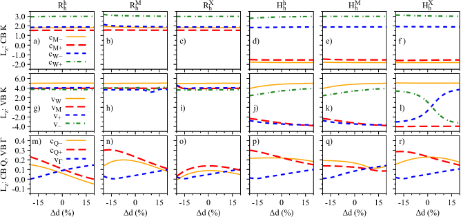
We now investigate the effect of external electric fields on the band edges of the R- and H-type stackings. In Fig. 3 we show the energy dependence of the relevant energy bands (see Fig. 1g) as function of the electric field with the color code of the K bands representing the layer-decomposition in the top row and the spin degree of freedom in the bottom row. Due to the particular symmetry of the energy bands (orbital and spin characters), the electric field can induce crossings or anti-crossings. The anti-crossings, visible in the top row of Fig. 3 when the color code deviates from red (WSe layer) or blue (MoSe layer), indicate regions with strong interlayer hybridization. Furthermore, these anti-crossings can either mix or preserve the spin degrees of freedom, depending on the stacking and bands involved. For instance, for the H stacking there is an anti-crossing between and (mainly localized at the WSe layer) that preserves spin. On the other hand, the anti-crossing of the R stacking between and (mainly localized at the WSe layer) also acts on the spin degree of freedom. We point out that the conduction bands at the Q point, shown by short dashed lines, do not present any crossing when the energy levels get closer as the values of electric field increase, as shown in the insets of Figs. 3g-l. The crossing of conduction bands takes place when electric field values are smaller than V/nm.
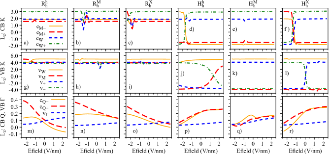
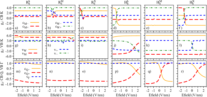
The electric field dependence of the quantities , , and that encode the essence of spin-valley physics is summarized in Figs. 4, 5 and 6, respectively. The most important feature revealed by our calculations is that , , and are strongly mixed around the anti-crossing regions shown in Fig. 3. In other words, spin and orbital degrees of freedom provide a clear quantitative signature for the strength of the interlayer coupling in these van der Waals heterostructures. Let us discuss in detail the case of H stacking, which shows the most prominent anti-crossing region for the valence bands and . The orbital and spin analysis in Fig. 3 reveal that and mix on the orbital level while the spin remains unchanged. Indeed, by inspecting Fig. 4j, we confirm that is unchanged for the interval of applied electric field. On the other hand, Fig. 5j shows that the values of are drastically modified as the electric field swipes through the anti-crossing region, with the strongest mixing happening at V/nm. In fact, already at zero electric field (as shown in Table 4) we clearly observe the hybridization effect taking place in the values of , suggesting that small values of applied electric field are enough to tune this hybridization even more. We point out that there are anti-crossing signatures also taking place in the conduction band. However, it seems that such feature has not been observed experimentally due to the range of electric field values appliedCiarrocchi et al. (2019); Baek et al. (2020); Barré et al. (2022). Additionally, the electric field introduces a strong change of the spin character in the conduction bands at the Q point due to their anti-crossing (insets of Figs. 3g-l), an interesting feature that can be investigated in low-energy interlayer excitonsBarré et al. (2022), which we discuss in further detail in Section IV.3. We note that the field-driven Rashba SOC is naturally incorporated within our first principles calculations. However, the electric field is just too weak to effectively remove spins from their out-of-plane direction.
Our detailed first-principles calculations reveal that the H stacking is the most suitable structure to investigate this interlayer hybridization signatures in the coupled spin-valley degrees of freedom. Surprisingly, this is the most stable structure for twist angles and the most relevant stacking for small twist angles, either having in mind a moiré or an atomically reconstructed sample, which facilitates the experimental accessibility to these effects. Furthermore, the opposite orientation of spin and orbital angular momenta from the opposite K-valleys in the individual monolayers favors g-factor variations from negative to positive values, for example, from to in the conduction band (Fig. 6d), from to in the valence band (Fig. 6j) and from to for conduction bands at the Q point (Fig. 6p).
III.3 Interlayer distance variation
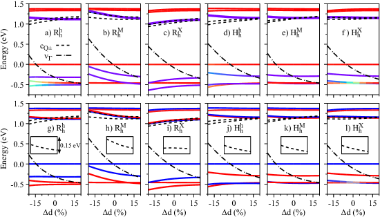
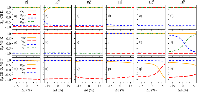
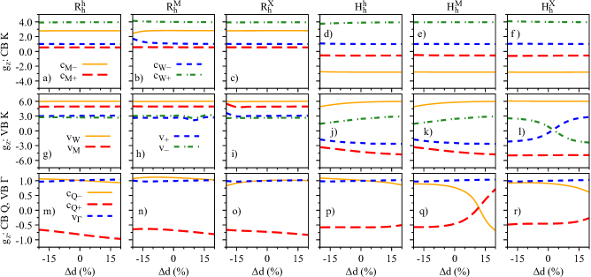
In this section we investigate the consequences of varying the equilibrium interlayer distance. This can be particularly relevant in the context of fluctuations introduced by the mechanical exfoliation and stamping procedures in TMDC heterostructuresNagler et al. (2017b); Plankl et al. (2021); Parzefall et al. (2021), which creates regions with good and bad interlayer contact. Additionally, changes in the interlayer distance can provide insights into the effects of external out-of-plane pressure, which can be currently investigated in available experimental setups, such as the recently reported studies on graphene/WSe2Fülöp et al. (2021), multilayered TMDCsOliva et al. (2022), and WSe/MoWSe heterostructuresKoo et al. (2023). On a more abstract and theoretical level, artificially varying the interlayer distance provides an additional knob to modify the interlayer hybridizationKunstmann et al. (2018) and analyze its impact on the spin and orbital angular momenta.
The influence of the interlayer distance variation on the energy levels, spin angular momenta, orbital angular momenta, and g-factors is presented in Figs. 7, 8, 9, and 10, respectively. We restrict ourselves to fluctuations of of the equilibrium interlayer distances given in Table 1. Overall, the same reasoning we discussed from the electric field effect applies to the interlayer distance variations. Nonetheless, we highlight a few points to strengthen the discussions and understanding presented in the previous Section III.2. There is a strong orbital mixing region visible in the lower valence bands with same spins in the R stacking case (Figs. 7a and 7g), but with a negligible signature in the (Fig. 9g) since the monolayer values of are all positive and close to each other. On the other hand, these hybridization effects are much stronger in the valence band of the H stacking case (Figs. 7f and 7l), with strong signatures in the values of and (Figs. 8l and 9l). We also mention that in the H stacking, the most favorable for the 60°case, the values of the valence band (particularly ) can be effectively altered by reducing the interlayer distance (also seen in the H stacking).
IV Low-energy dipolar excitons
In this section we investigate the fundamental ingredients that characterize the low-energy dipolar excitons, namely, the electric dipole moment, polarizability, dipole matrix elements and effective g-factors, based on the robust DFT calculations we presented in Sections II and III. External factors that can alter the energetic landscape of such dipolar excitons, and consequently their photoluminescence or reflectance spectra, are beyond the scope of the present manuscript. Regarding the spin-valley physics and g-factors, previous studies focusing on intralayer excitons in monolayer TMDCs show that DFT calculations indeed provide a remarkable agreement to experimental data for pristineRobert et al. (2021); Zinkiewicz et al. (2021) and strainedFaria Junior et al. (2022); Covre et al. (2022); Blundo et al. (2022) cases. These intralayer excitons have larger conduction-to-valence band dipole matrix elements, larger electron-hole exchange contributions, and weaker dielectric screening when compared to interlayer excitons. Therefore, if DFT is indeed capturing the relevant spin-valley properties of intralayer excitons, it will be sufficient enough to provide a reliable description of the spin-valley properties in dipolar excitons. In fact, DFT studies on interlayer exciton g-factorsWoźniak et al. (2020); Förste et al. (2020); Xuan and Quek (2020) are indeed capable of providing reliable comparison with experiments.
IV.1 Symmetry-based selection rules
Starting from the symmetry perspective, we can use the irreps computed in Section II to characterize the optical selection rules of the possible interlayer excitons. Let us first discuss the selection rules of direct excitons at the K points, in order to compare with and validate our DFT calculations in the next Section IV.3. Direct optical transitions are characterized by the matrix element mediated by the momentum operator
| (3) |
in which is the irrep of the initial (final) state and is the irrep of the momentum operator for a specific polarization (). The components of the momentum operator for circularly and linearly polarized light in the group transforms as
| (4) |
Combining Eq. 4 with the irreps of valence and conduction bands given in Table 2, we can compute the optical selection rules for K-K dipolar excitons. The results are shown in Table 5 and agree with previous symmetry-based and DFT calculationsYu et al. (2017); Wu et al. (2018); Woźniak et al. (2020). It is also possible to verify that the intralayer optical selection rules are nicely preserved. For instance, transitions from to provide , whereas transitions from to provide for R-type stackings and for H-type stackings. One important point to discuss here is related to the so-called spin-dark optical transitions (sometimes also refereed to as spin-flip or spin-singlet transitions), for instance, as the transition in the H stacking. The orientation of , given in Tables 3 and 4, is not a indicative of allowed or forbidden optical transitions. In fact, if we increase the number digits after the decimal point in Tables 3 and 4. This is already evident in the monolayer case due to the existence of the dark excitonsRobert et al. (2017); Molas et al. (2019); Zinkiewicz et al. (2020). The main point here is that SOC always introduces a mixing of spins (even in grapheneKurpas et al. (2019)) and that the momentum matrix element does not flip spin (more discussions about spin-mixing and optical transitions for spin-dark states in monolayer TMDCs can be found in Ref.Faria Junior et al. (2022)). Furthermore, some of the interlayer optical transitions presented in Table 5 have the same structure as the dark/grey excitons in monolayersRobert et al. (2017); Molas et al. (2019); Zinkiewicz et al. (2020), i. e., one transition with polarization and the other with . This feature actually explains the energy splitting of 0.1 meV experimentally observed at zero magnetic field by Li and coauthorsLi et al. (2022) in atomically reconstructed MoSe/WSe heterobilayers, akin to the dark-grey exciton splitting of 0.5 meV in pristine W-based monolayersRobert et al. (2017); Molas et al. (2019); Robert et al. (2017).
| R | ||
|---|---|---|
| R | ||
| R | ||
| H | ||
| H | ||
| H |
For optical transitions involving momentum-indirect dipolar excitons, i. e., transitions involving valence and conduction bands at different points, a phonon is required to ensure momentum conservation. The optical transition matrix element mediated by phonons is written asInui et al. (2012)
| (5) |
in which takes into account the electron-phonon coupling and transforms as the irrep . It is beyond the scope of this manuscript to provide deeper insights into the strength of the electron-phonon coupling but rather discuss qualitatively the possible symmetry-allowed mechanisms involving the momentum-indirect dipolar excitons.
| R | ||
|---|---|---|
| R | ||
| R | ||
| H | ||
| H | ||
| H |
For indirect excitons with electrons and holes in opposite K valleys (-K and K, sharing the same group), the direct product provides the output shown in Table 6. Notice that the output is always restricted to the irreps , , and . Phonons in the group would span all the irreps of the simple group, namely , , and . Combining the results given in Table 6 and performing a direct product with all possible phonon modes, we obtain
| (6) |
which always provides , , and . These irreps also encode the light polarization, as given in Eq. 4. What our results suggest is that any type of phonon with momentum K can, in principle, mediate the optical recombination of dipolar excitons with electrons and holes residing in opposite K valleys. Perhaps some of these processes are not favored due to off-resonant conditions and weak electron-phonon coupling, but could be effectively triggered once phonon energies are brought into resonance, such as the case of the 24T anomalyNagler et al. (2017b); Delhomme et al. (2020); Smirnov et al. (2022). Certainly, these phonon processes are intimately dependent on the strength of the electron-phonon couplings and how those couplings are translated for the final excitonic state (based on the particular conduction and valence bands constituents).
| R,R,R | H,H,H | |
|---|---|---|
| R | R | R | H | H | H | |
|---|---|---|---|---|---|---|
To investigate indirect dipolar excitons, with holes at the point and electrons at the K valley which do not have the same symmetry group, we must describe both conduction and valence band states in the same footing using compatibility relationsDresselhaus et al. (2007). It is more convenient to go from a higher symmetry group to a lower symmetry group then the other way around. With this in mind, we mapped point states to the K valley and present the direct product in Table 7. The same argument discussed in the case of electrons and holes at opposite valleys apply here, and multiple phonons with momentum K could trigger the optical recombination of such -K excitons.
Finally, we discuss the indirect excitons involving conduction bands at the Q point and holes at either or K points. Since the symmetry group contains a single irrep in the simple group, it means that all electronic states, phonon modes and operators are mapped into this irrep. Consequently, multiple phonon mediated processes are allowed. We note that Q-K transitions have been recently observedBarré et al. (2022), supporting the idea that some of these symmetry-allowed phonons discussed here are indeed favoring the optical recombination.
IV.2 Effective g-factors
Combining the band g-factors studied in Section III with the optical selection rules discussed in Section IV.1, we investigate here the effective g-factors of the relevant dipolar excitons. Since the momentum-indirect excitons require a phonon to mediate the optical emission, we can only determine unambiguously the sign of the g-factors for direct interlayer excitons, while for the other dipolar states we restrict ourselves to the magnitude of the g-factors. The dipolar exciton g-factors can be written as
| (7) |
in which and represent the conduction and valence band g-factors, and the sign contemplates the two possibilities of time-reversal partners. For example, interlayer excitons with the valence band and the conduction bands could be generated with and at the K point (direct in momentum), as indicated in Fig.1g or, with in the K point and in the K point (indirect in momentum).
The calculated g-factor values for the studied dipolar excitons are shown in Table 8. The largest absolute values stem from the KK dipolar excitons ( at K and at K in H-type, at -K and at K in R-type) since they involve the energy bands with largest g-factors. Some dipolar excitons show very similar g-factors, such as the values related to and excitons in H-type stackings. We also observed g-factors with values and even [], mainly originating from the valence bands at the point These different g-factors originated from different stackings and distinct dipolar exciton species could be observed in the cross-over region between deep and shallow moiré potentials as a function of the twist angle or temperature, however, no systematic experimental study has been realized to explore such conditions. We emphasize that our calculated values are in excellent agreement with previously reported theoretical studiesWoźniak et al. (2020); Xuan and Quek (2020); Gillen (2021); Zhao et al. (2022), and lie within the available experimental values, which range from -15 to -17 in H-type stackingsNagler et al. (2017b); Seyler et al. (2019); Wang et al. (2020); Delhomme et al. (2020); Mahdikhanysarvejahany et al. (2021); Förg et al. (2021); Holler et al. (2022); Smirnov et al. (2022); Li et al. (2022), and from 5 to 8 in R-type stackingsSeyler et al. (2019); Ciarrocchi et al. (2019); Joe et al. (2021); Mahdikhanysarvejahany et al. (2021); Holler et al. (2022); Smirnov et al. (2022); Li et al. (2022); Qian et al. (2023).
IV.3 Electric field dependence
We now turn to the behavior of the different dipolar excitons as a function of the electric field. Motivated by the experimentally accessible regimeCiarrocchi et al. (2019); Baek et al. (2020); Shanks et al. (2021); Barré et al. (2022); Shanks et al. (2022), in which there is no indication of any crossings in the top valence band or lower conduction bands, we restrict ourselves to electric field values V/nm, ensuring that the conduction band of MoSe is always below the conduction band of WSe. For positive values of electric field, there are no visible band crossings, so we can extend our analysis towards electric field values of V/nm. In fact, some experimental studies that investigate dipolar excitons under electric field also show an asymmetric rangeCiarrocchi et al. (2019); Baek et al. (2020); Barré et al. (2022), supporting the electric field values we consider here.
The energy dependence of the dipolar excitons under external electric fields can be directly inferred from the dependence of the energy bands, because the effective mass are barely affected by the electric field (changes on the order of ) and the dielectric environment remains unchanged. Therefore, the energy variation of the dipolar excitons with respect to the electric field can be extracted directly from the DFT calculationsPlankl et al. (2021) and modelled by the following dependenceRoch et al. (2018); Chakraborty et al. (2019)
| (8) |
in which is the electric dipole moment (in meV nm/V), is the polarizability (in meV nm2/V2), and is the electric field in V/nm.
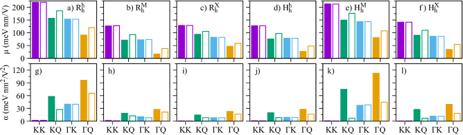
Our calculated values of the electric dipole moment and polarizabilities, fitted in the range of 0.7 to 0.7 V/nm, are presented in Fig. 11. Overall, our results reveal that the values of () decrease (increase) as we go from momentum-direct to momentum-indirect dipolar excitons (KK KQ K Q), reflecting the degree of layer delocalization of the bands involved ( Q K, as shown in Fig. 1a-f). These delocalization features have already been observed in the magnitude of interlayer excitons of WSe homobilayer structuresAltaiary et al. (2022); Huang et al. (2022) and there is one report on MoSe/WSe heterobilayersBarré et al. (2022). Our results also show that the spin-split conduction bands have negligible effect on and of KK and K excitons, whereas the conduction bands provide different signatures since they have different delocalization over the two layers. Particularly for the KK dipolar excitons, we note that the calculated values of are quite small ( meV nm2/V2) and the two possible excitons, stemming from , are nearly indistinguishable under the electric field dependence. However, they would have different emission energies (due to the SOC splitting of ) and distinct g-factor signatures. We note that our calculated values of for KK and KQ dipolar excitons, and particularly that are consistent with recent GW + Bethe-Salpeter calculations and experiments in MoSe/WSe heterobilayersBarré et al. (2022).
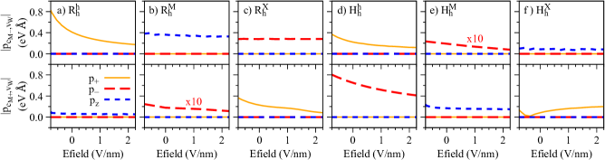
To validate the symmetry-based selection rules of direct interlayer excitons discussed in Section IV.1, we present the dipole matrix elements computed within DFT in Fig. 12. All the nonzero values match exactly the symmetry-based arguments discussed in Section IV.4. Generally, the dipole matrix elements decrease for increasing values of the electric field, with the exception of the that slightly increases for increasing electric field, reflecting the impact of the atomic registry on the wave functions of van der Waals heterostacks. Furthermore, the spin-dark optical transitions discussed in terms of symmetry in Section IV.1 are also present here. The momentum operator that enters the dipole matrix element (Eq. 4) does not flip spin and therefore this transition is optically bright only if the 2-component spinors are mixed, which is indeed the case in our first-principles calculations with SOC. Our calculated values of the dipole matrix elements, along with their respective polarization, can be readily used to generate massive Dirac models for the dipolar excitons via the first order perturbation within the k.p formalism, allowing the investigation of spin-dependent physics beyond the parabolic approximationWu et al. (2018); Erkensten et al. (2021).
Based on the calculated values of the energy dependence and dipole matrix elements with respect to the electric field, we can evaluate the radiative lifetime for direct dipolar excitons, given byGlazov et al. (2014, 2015)
| (9) |
with being high-frequency dielectric constant of the environment, is the speed of light, is the reduced Plank constant, is the electron charge, is the exciton energy, and is the exciton envelope function evaluated at the origin. The relevant quantities that depend on the electric field, , are the exciton energy, (see Eq. 1) and the dipole matrix element, (see Fig. 12). Typical interlayer excitons exhibit lifetimes reaching almost 100 ns at very low temperatures and a few ns at room temperatureRivera et al. (2015); Miller et al. (2017); Nagler et al. (2017a), with roughly one order of magnitude fluctuation when comparing different samples. To understand the isolated impact of the electric field on the radiative lifetime of the direct dipolar excitons, we consider the quantity
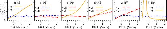
| (10) |
and display its calculated values in Fig. 13 as function of the electric field. The calculated ratio varies in general in the range of 0.5 to 4.5, except for the case H that shows a drastic increase of the radiative lifetime because the dipole matrix element decreases to nearly zero in Fig. 12f. Particularly for the high-symmetry stacking H, which is the most favorable one for 60° samples, both direct dipolar excitons (singlet and triplet) exhibit an increase in the radiative lifetime as the electric field increases, which can be accessed experimentally in current devices.
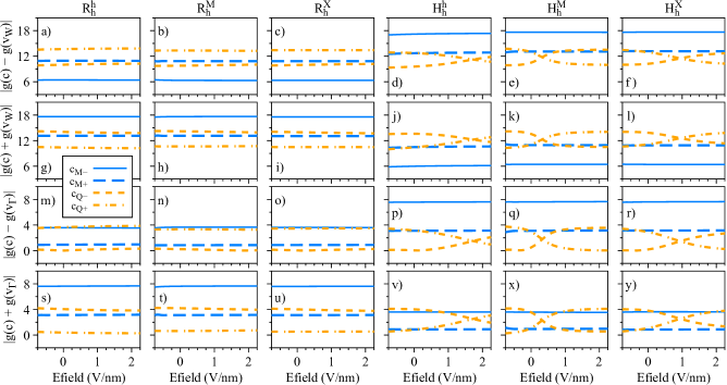
Let us now discuss electric field effects on the valley Zeeman physics of the dipolar excitons (schematically shown in Fig. 1g). The effective g-factors calculated via Eq. 7 as a function of the electric field are shown in Fig. 14 for all the considered R- and H-type stackings. Our results reveal that these dipolar excitons have a very robust valley Zeeman, barely changing under external electric field. The only exception are the dipolar excitons involving Q bands in the H-type stackings. Because of the g-factor crossing between and bands (see Figs. 6p,q,r) stemming from spin mixing effects (see Figs. 4p,q,r and Figs. 5p,q,r), the valley Zeeman of these indirect dipolar excitons is consequently affected and exhibits pronounced changes for increasing electric fields (see Figs. 14d-f,j-l,p-r,v-y). Therefore, without significant band hybridization the dipolar excitons retain their valley Zeeman signatures over a large range of applied electric field values, which can be particularly relevant for electrically-driven opto-spintronics applicationsSierra et al. (2021). In fact, our results reveal very fundamental and general features about the valley Zeeman mixing of excitonic states (including dipolar excitons) in 2D materials and van der Waals heterostructures, in this case, stemming from the band hybridization between different layers. Clear signatures of the valley Zeeman mixing on the excitonic states are still rather limited, but have been already observed experimentally in a few systems, namely, strained WS2 monolayersBlundo et al. (2022), defect-mediated excitons in MoS2 monolayersAmit et al. (2022); Hötger et al. (2022), WS2/graphene heterostructuresFaria Junior et al. (2023) and electrically-controlled trilayer MoSe2 structuresFeng et al. (2022).
IV.4 Interlayer distance variation
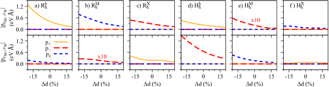
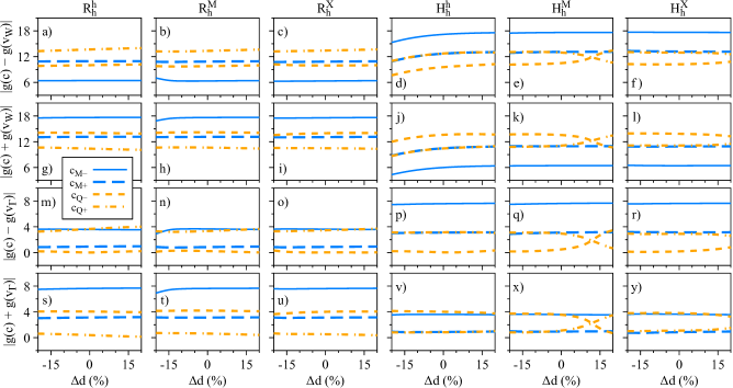
In this section we focus on the effect of the interlayer distance variation. Our calculated values of the dipole matrix elements and the g-factors are presented in Fig. 15 and Fig. 16, respectively, and follow the same convention as discussed in the case of the electric field (Figs. 12 and 14). Particularly, we found a strong decrease of the dipole matrix elements as the interlayer distance increases, consequently making the dipolar excitons less optically active. These findings provide support to the idea that weakly coupled heterobilayers (with an interlayer separation larger than the equilibrium distance), with perhaps additional electric field displacements due to asymmetric bottom and top environments, may exhibit highly quenched optical emission of dipolar excitonsPlankl et al. (2021); Parzefall et al. (2021). Furthermore, since the dipole matrix elements behave in a similar fashion as the electric field we expect similar behavior for the quantity . Another interesting aspect, visible in the H stacking, is the decrease of the valley Zeeman originating from the top valence band at the K point, , as the interlayer distance decreases (Figs. 16d,j). We believe this feature can be experimentally probed using external pressureFülöp et al. (2021); Oliva et al. (2022), which effectively decreases the interlayer distance. For the H stacking, we also observe the signatures of Q-band mixing and reversal of the g-factor values as the interlayer distance increases.
V Concluding remarks
In summary, we performed detailed first-principles calculations on the spin-valley physics of MoSe/WSe heterobilayers under the effect of out-of-plane electric fields and as a function of the interlayer separation. Specifically, we investigated the spin and orbital degrees of freedom, g-factors, and symmetry properties of the relevant band edges (located at the K, Q and points) of high-symmetry stackings with 0°(R-type) and 60°(H-type) twist angles. These R- and H-type stackings are the fundamental building blocks present in moiré and atomically reconstructed supercells, experimentally observed in samples with small twist angles. Our calculations reveal distinct hybridization signatures of the spin and orbital degrees of freedom as a function of the electric field and interlayer separation, depending on the energy band and on the stacking configuration. With this crucial knowledge of the spin-valley physics of the band edges, we expanded our analysis to the low-energy dipolar (interlayer) excitons, either direct or indirect in -space. We found that these different dipolar exciton species present distinct electric dipole moments, polarizabilities, and valley Zeeman signatures (g-factors) due to the particular mixing of the spin and orbital angular momenta from their constituent energy bands. We also perform a symmetry analysis to discuss the phonon modes that could mediate the optical recombination of momentum-indirect dipolar excitons. Regarding the valley Zeeman signatures of the interlayer excitonic states, our calculations reveal that direct dipolar excitons at the K-valley carry a robust valley Zeeman effect nearly independent of the electric field. On the other hand, the momentum-indirect dipolar excitons in the H-type stackings, with valence band at the K valleys and conduction bands at the Q valleys, show a pronounced dependence of the valley Zeeman for positive values of applied electric fields. This peculiar g-factor dependence is unambiguously related to the spin-mixing of conduction bands at the Q point, which is absent in the R-type stackings. The valley Zeeman physics of the investigated dipolar excitons can also be affected by varying the interlayer distance, which could be experimentally probed under external pressure. As in the case of external electric fields, the interlayer variation effects in the valley Zeeman signatures are more pronounced in H-type stackings and are more likely to be observed in samples with twist angle close to 60.
Although the intralayer excitons were not in the scope of the present manuscript, these quasiparticles are still optically active and easily recognized in the photoluminescence or reflectivity spectra of MoSe/WSe heterobilayersRivera et al. (2015); Nagler et al. (2017b); Gobato et al. (2022). Particularly, our g-factor calculations for the band edges (Fig. 6) suggest that intralayer excitons could also provide valuable information on the interlayer hybridization via the valley Zeeman as a function of the electric field. Gated devices based of MoSe/WSe heterostructures are within experimental reachCiarrocchi et al. (2019); Shanks et al. (2022); Ciarrocchi et al. (2022) and could be used to test our hypothesis. We note that, in order to properly evaluate the intralayer exciton physics, it would be desirable to go beyond DFT calculations and employ the GW + Bethe-Salpeter formalismDeilmann and Thygesen (2018); Deilmann et al. (2020); Barré et al. (2022); Amit et al. (2022), which is beyond the scope of this work. Nonetheless, since these intralayer excitons are also quite localized in -spaceChernikov et al. (2014); Wang et al. (2018); Faria Junior et al. (2023), the spin and orbital angular momenta of the Bloch bands should account for the majority of the hybridization effects.
We emphasize that the theoretical approach employed here in our study is quite robust and provides quantitative microscopic insights into the spin-valley physics of these van der Waals heterobilayers. This framework can certainly be extended to more complex multilayered van der Waals heterostructures that also host dipolar excitons, for instance, large-angle twisted MoSe2/WS2McDonnell et al. (2020); Volmer et al. (2022), homobilayersDeilmann and Thygesen (2018); Lin et al. (2021), trilayer hetero- and homo-structuresLi et al. (2021); Feng et al. (2022); Zhang et al. (2022), and MoSe2/WS2 heterobilayersAlexeev et al. (2019); Tang et al. (2020); Gobato et al. (2022).
Acknowledgements.
We thank Yaroslav Zhumagulov and Christian Schüller for helpful discussions and Sivan Refaely-Abramson for valuable insights into interlayer excitons. The authors acknowledge the financial support of the Deutsche Forschungsgemeinschaft (DFG, German Research Foundation) SFB 1277 (Project-ID 314695032, projects B07 and B11), SPP 2244 (Project No. 443416183) and of the European Union Horizon 2020 Research and Innovation Program under Contract No. 881603 (Graphene Flagship).Appendix A: Computational details
The DFT are performed using the WIEN2k codeBlaha et al. (2020), which implements a full potential all-electron scheme with augmented plane wave plus local orbitals (APW+lo) method. The crystal structures of monolayers and the heterostructure are generated using the atomic simulation environment (ASE) python packageBahn and Jacobsen (2002). We used the Perdew-Burke-Ernzerhof exchange-correlation functionalPerdew et al. (1996), a Monkhorst-Pack k-grid of 1515 and a self-consistent convergence criteria of 10-6 e for the charge and 10-6 Ry for the energy. For the heterostructures, van der Waals corrections3Grimme et al. (2010) are taken into account in the self-consistent cycle. The core–valence energy separation is chosen as Ry, the atomic spheres are expanded in orbital quantum numbers up to 10 and the plane-wave cutoff multiplied by the smallest atomic radii is set to 9. For the inclusion of SOC, core electrons are considered fully relativistically whereas valence electrons are treated in a second variational stepSingh and Nordstrom (2006), with the scalar-relativistic wave functions calculated in an energy window of -10 to 8 Ry. This upper energy limit provides a sufficiently large number of bands ( 1500) to guarantee the proper convergence of the orbital angular momentum, as shown in Refs. Woźniak et al. (2020); Förste et al. (2020); Faria Junior et al. (2022). The applied out-of-plane electric field is included as a zig-zag potential added to the exchange-correlation functionalStahn et al. (2001) with 40 Fourier coefficients. The structural parameters are discussed in Section II.
References
- Mak et al. (2010) K. F. Mak, C. Lee, J. Hone, J. Shan, and T. F. Heinz, Phys. Rev. Lett. 105, 136805 (2010).
- Splendiani et al. (2010) A. Splendiani, L. Sun, Y. Zhang, T. Li, J. Kim, C.-Y. Chim, G. Galli, and F. Wang, Nano Lett. 10, 1271 (2010).
- Kuc et al. (2011) A. Kuc, N. Zibouche, and T. Heine, Phys. Rev. B 83, 245213 (2011).
- Kumar and Ahluwalia (2012) A. Kumar and P. Ahluwalia, The European Physical Journal B 85, 186 (2012).
- Xiao et al. (2012) D. Xiao, G.-B. Liu, W. Feng, X. Xu, and W. Yao, Phys. Rev. Lett. 108, 196802 (2012).
- Mak et al. (2012) K. F. Mak, K. He, J. Shan, and T. F. Heinz, Nature Nanotechnology 7, 494 (2012).
- Mak et al. (2014) K. F. Mak, K. L. McGill, J. Park, and P. L. McEuen, Science 344, 1489 (2014).
- Qiu et al. (2013) D. Y. Qiu, F. H. da Jornada, and S. G. Louie, Physical Review Letters 111, 216805 (2013).
- Xu et al. (2014) X. Xu, W. Yao, D. Xiao, and T. F. Heinz, Nature Physics 10, 343 (2014).
- Chernikov et al. (2014) A. Chernikov, T. C. Berkelbach, H. M. Hill, A. Rigosi, Y. Li, O. B. Aslan, D. R. Reichman, M. S. Hybertsen, and T. F. Heinz, Phys. Rev. Lett. 113, 076802 (2014).
- Stier et al. (2016) A. V. Stier, K. M. McCreary, B. T. Jonker, J. Kono, and S. A. Crooker, Nature Commun. 7, 10643 (2016).
- Schaibley et al. (2016) J. R. Schaibley, H. Yu, G. Clark, P. Rivera, J. S. Ross, K. L. Seyler, W. Yao, and X. Xu, Nature Reviews Materials 1, 16055 (2016).
- Raja et al. (2017) A. Raja, A. Chaves, J. Yu, G. Arefe, H. M. Hill, A. F. Rigosi, T. C. Berkelbach, P. Nagler, C. Schüller, T. Korn, C. Nuckolls, J. Hone, L. E. Brus, T. F. Heinz, D. R. Reichman, and A. Chernikov, Nature Commun. 8, 15251 (2017).
- Wang et al. (2018) G. Wang, A. Chernikov, M. M. Glazov, T. F. Heinz, X. Marie, T. Amand, and B. Urbaszek, Rev. Mod. Phys. 90, 021001 (2018).
- Geim and Grigorieva (2013) A. K. Geim and I. V. Grigorieva, Nature 499, 419 (2013).
- Song and Gabor (2018) J. C. W. Song and N. M. Gabor, Nature Nanotechnology 13, 986 (2018).
- Sierra et al. (2021) J. F. Sierra, J. Fabian, R. K. Kawakami, S. Roche, and S. O. Valenzuela, Nature Nanotechnology 16, 856 (2021).
- Ciarrocchi et al. (2022) A. Ciarrocchi, F. Tagarelli, A. Avsar, and A. Kis, Nature Reviews Materials 7, 449 (2022).
- Tran et al. (2019) K. Tran, G. Moody, F. Wu, X. Lu, J. Choi, K. Kim, A. Rai, D. A. Sanchez, J. Quan, A. Singh, et al., Nature 567, 71 (2019).
- Seyler et al. (2019) K. L. Seyler, P. Rivera, H. Yu, N. P. Wilson, E. L. Ray, D. G. Mandrus, J. Yan, W. Yao, and X. Xu, Nature 567, 66 (2019).
- Leisgang et al. (2020) N. Leisgang, S. Shree, I. Paradisanos, L. Sponfeldner, C. Robert, D. Lagarde, A. Balocchi, K. Watanabe, T. Taniguchi, X. Marie, R. J. Warburton, I. C. Gerber, and B. Urbaszek, Nature Nanotechnology 15, 901 (2020).
- Lin et al. (2021) K.-Q. Lin, P. E. Faria Junior, J. M. Bauer, B. Peng, B. Monserrat, M. Gmitra, J. Fabian, S. Bange, and J. M. Lupton, Nature Commun. 12, 1553 (2021).
- Gmitra and Fabian (2015) M. Gmitra and J. Fabian, Physical Review B 92, 155403 (2015).
- Gmitra et al. (2016) M. Gmitra, D. Kochan, P. Högl, and J. Fabian, Physical Review B 93, 155104 (2016).
- Avsar et al. (2017) A. Avsar, D. Unuchek, J. Liu, O. L. Sanchez, K. Watanabe, T. Taniguchi, B. Özyilmaz, and A. Kis, ACS Nano 11, 11678 (2017).
- Luo et al. (2017) Y. K. Luo, J. Xu, T. Zhu, G. Wu, E. J. McCormick, W. Zhan, M. R. Neupane, and R. K. Kawakami, Nano Lett. 17, 3877 (2017).
- Faria Junior et al. (2023) P. E. Faria Junior, T. Naimer, K. M. McCreary, B. T. Jonker, J. J. Finley, S. Crooker, J. Fabian, and A. V. Stier, arXiv preprint arXiv:2301.12234 (2023), 10.48550/arXiv:2301.12234.
- Cadiz et al. (2017) F. Cadiz, E. Courtade, C. Robert, G. Wang, Y. Shen, H. Cai, T. Taniguchi, K. Watanabe, H. Carrere, D. Lagarde, M. Manca, T. Amand, P. Renucci, S. Tongay, X. Marie, and B. Urbaszek, Phys. Rev. X 7, 021026 (2017).
- Goryca et al. (2019) M. Goryca, J. Li, A. V. Stier, T. Taniguchi, K. Watanabe, E. Courtade, S. Shree, C. Robert, B. Urbaszek, X. Marie, and S. A. Crooker, Nature Commun. 10, 4172 (2019).
- Yankowitz et al. (2019) M. Yankowitz, Q. Ma, P. Jarillo-Herrero, and B. J. LeRoy, Nature Reviews Physics 1, 112 (2019).
- Zollner et al. (2019a) K. Zollner, P. E. Faria Junior, and J. Fabian, Phys. Rev. B 100, 085128 (2019a).
- Zollner et al. (2023) K. Zollner, P. E. Faria Junior, and J. Fabian, Phys. Rev. B 107, 035112 (2023).
- Zhong et al. (2017) D. Zhong, K. L. Seyler, X. Linpeng, R. Cheng, N. Sivadas, B. Huang, E. Schmidgall, T. Taniguchi, K. Watanabe, M. A. McGuire, W. Yao, D. Xiao, K.-M. C. Fu, and X. Xu, Sci. Adv. 3, e1603113 (2017).
- Ciorciaro et al. (2020) L. Ciorciaro, M. Kroner, K. Watanabe, T. Taniguchi, and A. Imamoglu, Physical Review Letters 124, 197401 (2020).
- Choi et al. (2022) J. Choi, C. Lane, J.-X. Zhu, and S. A. Crooker, Nature Materials (2022), 10.1038/s41563-022-01424-w.
- Chaves et al. (2018) A. Chaves, J. G. Azadani, V. O. Özçelik, R. Grassi, and T. Low, Phys. Rev. B 98, 121302 (2018).
- Gillen and Maultzsch (2018) R. Gillen and J. Maultzsch, Phys. Rev. B 97, 165306 (2018).
- Torun et al. (2018) E. Torun, H. P. C. Miranda, A. Molina-Sánchez, and L. Wirtz, Phys. Rev. B 97, 245427 (2018).
- Rivera et al. (2015) P. Rivera, J. R. Schaibley, A. M. Jones, J. S. Ross, S. Wu, G. Aivazian, P. Klement, K. Seyler, G. Clark, N. J. Ghimire, J. Yan, D. G. Mandrus, W. Yao, and X. Xu, Nature Commun. 6, 6242 (2015).
- Miller et al. (2017) B. Miller, A. Steinhoff, B. Pano, J. Klein, F. Jahnke, A. Holleitner, and U. Wurstbauer, Nano Letters 17, 5229 (2017).
- Nagler et al. (2017a) P. Nagler, G. Plechinger, M. V. Ballottin, A. Mitioglu, S. Meier, N. Paradiso, C. Strunk, A. Chernikov, P. C. M. Christianen, C. Schüller, and T. Korn, 2D Materials 4, 025112 (2017a).
- Ciarrocchi et al. (2019) A. Ciarrocchi, D. Unuchek, A. Avsar, K. Watanabe, T. Taniguchi, and A. Kis, Nature Photonics 13, 131 (2019).
- Baek et al. (2020) H. Baek, M. Brotons-Gisbert, Z. X. Koong, A. Campbell, M. Rambach, K. Watanabe, T. Taniguchi, and B. D. Gerardot, Science Advances 6, eaba8526 (2020).
- Shanks et al. (2021) D. N. Shanks, F. Mahdikhanysarvejahany, C. Muccianti, A. Alfrey, M. R. Koehler, D. G. Mandrus, T. Taniguchi, K. Watanabe, H. Yu, B. J. LeRoy, and J. R. Schaibley, Nano Letters 21, 5641 (2021).
- Barré et al. (2022) E. Barré, O. Karni, E. Liu, A. L. O’Beirne, X. Chen, H. B. Ribeiro, L. Yu, B. Kim, K. Watanabe, T. Taniguchi, K. Barmak, C. H. Lui, S. Refaely-Abramson, F. H. da Jornada, and T. F. Heinz, Science 376, 406 (2022).
- Shanks et al. (2022) D. N. Shanks, F. Mahdikhanysarvejahany, T. G. Stanfill, M. R. Koehler, D. G. Mandrus, T. Taniguchi, K. Watanabe, B. J. LeRoy, and J. R. Schaibley, Nano Letters 22, 6599 (2022).
- Nagler et al. (2017b) P. Nagler, M. V. Ballottin, A. A. Mitioglu, F. Mooshammer, N. Paradiso, C. Strunk, R. Huber, A. Chernikov, P. C. M. Christianen, C. Schüller, and T. Korn, Nature Commun. 8, 1551 (2017b).
- Mahdikhanysarvejahany et al. (2021) F. Mahdikhanysarvejahany, D. N. Shanks, C. Muccianti, B. H. Badada, I. Idi, A. Alfrey, S. Raglow, M. R. Koehler, D. G. Mandrus, T. Taniguchi, K. Watanabe, O. L. A. Monti, H. Yu, B. J. LeRoy, and J. R. Schaibley, npj 2D Materials and Applications 5, 67 (2021).
- Holler et al. (2022) J. Holler, M. Selig, M. Kempf, J. Zipfel, P. Nagler, M. Katzer, F. Katsch, M. V. Ballottin, A. A. Mitioglu, A. Chernikov, P. C. M. Christianen, C. Schüller, A. Knorr, and T. Korn, Phys. Rev. B 105, 085303 (2022).
- Smirnov et al. (2022) D. S. Smirnov, J. Holler, M. Kempf, J. Zipfel, P. Nagler, M. V. Ballottin, A. A. Mitioglu, A. Chernikov, P. C. M. Christianen, C. Schüller, and T. Korn, 2D Materials 9, 045016 (2022).
- Li et al. (2022) Z. Li, F. Tabataba-Vakili, S. Zhao, A. Rupp, I. Bilgin, Z. Herdegen, B. März, K. Watanabe, T. Taniguchi, G. R. Schleder, A. S. Baimuratov, E. Kaxiras, K. Müller-Caspary, and A. Högele, arXiv preprint arXiv:2212.07686 (2022), 10.48550/arXiv:2212.07686.
- Choi et al. (2021) J. Choi, M. Florian, A. Steinhoff, D. Erben, K. Tran, D. S. Kim, L. Sun, J. Quan, R. Claassen, S. Majumder, J. A. Hollingsworth, T. Taniguchi, K. Watanabe, K. Ueno, A. Singh, G. Moody, F. Jahnke, and X. Li, Phys. Rev. Lett. 126, 047401 (2021).
- Förg et al. (2021) M. Förg, A. S. Baimuratov, S. Y. Kruchinin, I. A. Vovk, J. Scherzer, J. Förste, V. Funk, K. Watanabe, T. Taniguchi, and A. Högele, Nature Commun. 12, 1656 (2021).
- Enaldiev et al. (2020) V. V. Enaldiev, V. Zólyomi, C. Yelgel, S. J. Magorrian, and V. I. Fal’ko, Phys. Rev. Lett. 124, 206101 (2020).
- Holler et al. (2020) J. Holler, S. Meier, M. Kempf, P. Nagler, K. Watanabe, T. Taniguchi, T. Korn, and C. Schüller, Applied Physics Letters 117, 013104 (2020).
- Parzefall et al. (2021) P. Parzefall, J. Holler, M. Scheuck, A. Beer, K.-Q. Lin, B. Peng, B. Monserrat, P. Nagler, M. Kempf, T. Korn, et al., 2D Materials 8, 035030 (2021).
- Zhao et al. (2022) S. Zhao, X. Huang, Z. Li, A. Rupp, J. Göser, I. A. Vovk, S. Y. Kruchinin, K. Watanabe, T. Taniguchi, I. Bilgin, A. S. Baimuratov, and A. Högele, arXiv preprint arXiv:2202.11139 (2022), 10.48550/arXiv:2202.11139.
- Hanbicki et al. (2018) A. T. Hanbicki, H.-J. Chuang, M. R. Rosenberger, C. S. Hellberg, S. V. Sivaram, K. M. McCreary, I. I. Mazin, and B. T. Jonker, ACS Nano 12, 4719 (2018).
- Sigl et al. (2020) L. Sigl, F. Sigger, F. Kronowetter, J. Kiemle, J. Klein, K. Watanabe, T. Taniguchi, J. J. Finley, U. Wurstbauer, and A. W. Holleitner, Phys. Rev. Res. 2, 042044 (2020).
- Wang et al. (2020) T. Wang, S. Miao, Z. Li, Y. Meng, Z. Lu, Z. Lian, M. Blei, T. Taniguchi, K. Watanabe, S. Tongay, D. Smirnov, and S.-F. Shi, Nano Letters 20, 694 (2020).
- Delhomme et al. (2020) A. Delhomme, D. Vaclavkova, A. Slobodeniuk, M. Orlita, M. Potemski, D. M. Basko, K. Watanabe, T. Taniguchi, D. Mauro, C. Barreteau, E. Giannini, A. F. Morpurgo, N. Ubrig, and C. Faugeras, 2D Materials 7, 041002 (2020).
- Ramasubramaniam et al. (2011) A. Ramasubramaniam, D. Naveh, and E. Towe, Phys. Rev. B 84, 205325 (2011).
- Plankl et al. (2021) M. Plankl, P. E. Faria Junior, F. Mooshammer, T. Siday, M. Zizlsperger, F. Sandner, F. Schiegl, S. Maier, M. A. Huber, M. Gmitra, J. Fabian, J. L. Boland, T. L. Cocker, and R. Huber, Nature Photonics 15, 594 (2021).
- Woźniak et al. (2020) T. Woźniak, P. E. Faria Junior, G. Seifert, A. Chaves, and J. Kunstmann, Phys. Rev. B 101, 235408 (2020).
- Deilmann et al. (2020) T. Deilmann, P. Krüger, and M. Rohlfing, Phys. Rev. Lett. 124, 226402 (2020).
- Förste et al. (2020) J. Förste, N. V. Tepliakov, S. Y. Kruchinin, J. Lindlau, V. Funk, M. Förg, K. Watanabe, T. Taniguchi, A. S. Baimuratov, and A. Högele, Nature Commun. 11, 4539 (2020).
- Xuan and Quek (2020) F. Xuan and S. Y. Quek, Phys. Rev. Research 2, 033256 (2020).
- Yu et al. (2015) H. Yu, Y. Wang, Q. Tong, X. Xu, and W. Yao, Phys. Rev. Lett. 115, 187002 (2015).
- Yu et al. (2017) H. Yu, G.-B. Liu, J. Tang, X. Xu, and W. Yao, Science Advances 3 (2017), 10.1126/sciadv.1701696.
- Nieken et al. (2022) R. Nieken, A. Roche, F. Mahdikhanysarvejahany, T. Taniguchi, K. Watanabe, M. R. Koehler, D. G. Mandrus, J. Schaibley, and B. J. LeRoy, APL Materials 10, 031107 (2022).
- Wu et al. (2017) F. Wu, T. Lovorn, and A. H. MacDonald, Phys. Rev. Lett. 118, 147401 (2017).
- Yu et al. (2018) H. Yu, G.-B. Liu, and W. Yao, 2D Materials 5, 035021 (2018).
- Wu et al. (2018) F. Wu, T. Lovorn, and A. H. MacDonald, Phys. Rev. B 97, 035306 (2018).
- Ruiz-Tijerina et al. (2020) D. A. Ruiz-Tijerina, I. Soltero, and F. Mireles, Phys. Rev. B 102, 195403 (2020).
- Erkensten et al. (2021) D. Erkensten, S. Brem, and E. Malic, Phys. Rev. B 103, 045426 (2021).
- Kormányos et al. (2015) A. Kormányos, G. Burkard, M. Gmitra, J. Fabian, V. Zólyomi, N. D. Drummond, and V. Fal’ko, 2D Materials 2, 022001 (2015).
- Zollner et al. (2019b) K. Zollner, P. E. Faria Junior, and J. Fabian, Phys. Rev. B 100, 195126 (2019b).
- Nayak et al. (2017) P. K. Nayak, Y. Horbatenko, S. Ahn, G. Kim, J.-U. Lee, K. Y. Ma, A.-R. Jang, H. Lim, D. Kim, S. Ryu, et al., ACS Nano 11, 4041 (2017).
- Xu et al. (2018) K. Xu, Y. Xu, H. Zhang, B. Peng, H. Shao, G. Ni, J. Li, M. Yao, H. Lu, H. Zhu, and C. M. Soukoulis, Physical Chemistry Chemical Physics 20, 30351 (2018).
- Gillen (2021) R. Gillen, physica status solidi (b) 258, 2000614 (2021).
- Blaha et al. (2020) P. Blaha, K. Schwarz, F. Tran, R. Laskowski, G. K. Madsen, and L. D. Marks, The Journal of Chemical Physics 152, 074101 (2020).
- Song and Dery (2013) Y. Song and H. Dery, Phys. Rev. Lett. 111, 026601 (2013).
- Dery and Song (2015) H. Dery and Y. Song, Phys. Rev. B 92, 125431 (2015).
- Gilardoni et al. (2021) C. M. Gilardoni, F. Hendriks, C. H. van der Wal, and M. H. D. Guimarães, Phys. Rev. B 103, 115410 (2021).
- Blundo et al. (2022) E. Blundo, P. E. Faria Junior, A. Surrente, G. Pettinari, M. A. Prosnikov, K. Olkowska-Pucko, K. Zollner, T. Woźniak, A. Chaves, T. Kazimierczuk, M. Felici, A. Babiński, M. R. Molas, P. C. M. Christianen, J. Fabian, and A. Polimeni, Phys. Rev. Lett. 129, 067402 (2022).
- Dresselhaus (1955) G. Dresselhaus, Phys. Rev. 100, 580 (1955).
- Kane (1966) E. O. Kane, Physics of III-V compounds, Semiconductors and Semimetals, Vol. 1 (Academic Press, New York, 1966).
- Kane (1957) E. O. Kane, Journal of Physics and Chemistry of Solids 1, 249 (1957).
- Dresselhaus et al. (2007) M. S. Dresselhaus, G. Dresselhaus, and A. Jorio, Group theory: application to the physics of condensed matter (Springer Science & Business Media, 2007).
- Lew Yan Voon and Willatzen (2009) L. C. Lew Yan Voon and M. Willatzen, The k.p method: electronic properties of semiconductors (Springer, Berlin, 2009).
- Koster et al. (1963) G. F. Koster, J. O. Dimmock, R. G. Wheeler, and H. Statz, Properties of the thirty-two point groups, Vol. 24 (MIT press, 1963).
- Xuan and Quek (2021) F. Xuan and S. Y. Quek, npj Computational Materials 7, 198 (2021).
- Heißenbüttel et al. (2021) M.-C. Heißenbüttel, T. Deilmann, P. Krüger, and M. Rohlfing, Nano Letters 21, 5173 (2021).
- Covre et al. (2022) F. S. Covre, P. E. Faria Junior, V. O. Gordo, C. S. de Brito, Y. V. Zhumagulov, M. D. Teodoro, O. D. D. Couto, L. Misoguti, S. Pratavieira, M. B. Andrade, P. C. M. Christianen, J. Fabian, F. Withers, and Y. Galvão Gobato, Nanoscale 14, 5758 (2022).
- Faria Junior et al. (2022) P. E. Faria Junior, K. Zollner, T. Woźniak, M. Kurpas, M. Gmitra, and J. Fabian, New Journal of Physics 24, 083004 (2022).
- Raiber et al. (2022) S. Raiber, P. E. Faria Junior, D. Falter, S. Feldl, P. Marzena, K. Watanabe, T. Taniguchi, J. Fabian, and C. Schüller, Nature Communications 13, 4997 (2022).
- Amit et al. (2022) T. Amit, D. Hernangómez-Pérez, G. Cohen, D. Y. Qiu, and S. Refaely-Abramson, Phys. Rev. B 106, L161407 (2022).
- Hötger et al. (2022) A. Hötger, T. Amit, J. Klein, K. Barthelmi, T. Pelini, A. Delhomme, S. Rey, M. Potemski, C. Faugeras, G. Cohen, D. Hernangómez-Pérez, T. Taniguchi, K. Watanabe, C. Kastl, J. J. Finley, S. Refaely-Abramson, A. W. Holleitner, and A. V. Stier, arXiv preprint arXiv:2205.10286 (2022), 10.48550/arXiv:2205.10286.
- Gobato et al. (2022) Y. G. Gobato, C. S. de Brito, A. Chaves, M. A. Prosnikov, T. Woźniak, S. Guo, I. D. Barcelos, M. V. Milošević, F. Withers, and P. C. M. Christianen, Nano Letters 22, 8641 (2022).
- Lejaeghere et al. (2016) K. Lejaeghere, G. Bihlmayer, T. Björkman, P. Blaha, S. Blügel, V. Blum, D. Caliste, I. E. Castelli, S. J. Clark, A. D. Corso, S. de Gironcoli, T. Deutsch, J. K. Dewhurst, I. D. Marco, C. Draxl, M. Dułak, O. Eriksson, J. A. Flores-Livas, K. F. Garrity, L. Genovese, P. Giannozzi, M. Giantomassi, S. Goedecker, X. Gonze, O. Grånäs, E. K. U. Gross, A. Gulans, F. Gygi, D. R. Hamann, P. J. Hasnip, N. A. W. Holzwarth, D. Iuşan, D. B. Jochym, F. Jollet, D. Jones, G. Kresse, K. Koepernik, E. Küçükbenli, Y. O. Kvashnin, I. L. M. Locht, S. Lubeck, M. Marsman, N. Marzari, U. Nitzsche, L. Nordström, T. Ozaki, L. Paulatto, C. J. Pickard, W. Poelmans, M. I. J. Probert, K. Refson, M. Richter, G.-M. Rignanese, S. Saha, M. Scheffler, M. Schlipf, K. Schwarz, S. Sharma, F. Tavazza, P. Thunström, A. Tkatchenko, M. Torrent, D. Vanderbilt, M. J. van Setten, V. V. Speybroeck, J. M. Wills, J. R. Yates, G.-X. Zhang, and S. Cottenier, Science 351, aad3000 (2016).
- Gmitra et al. (2009) M. Gmitra, S. Konschuh, C. Ertler, C. Ambrosch-Draxl, and J. Fabian, Physical Review B 80, 235431 (2009).
- Konschuh et al. (2010) S. Konschuh, M. Gmitra, and J. Fabian, Physical Review B 82, 245412 (2010).
- Kurpas et al. (2016) M. Kurpas, M. Gmitra, and J. Fabian, Physical Review B 94, 155423 (2016).
- Kurpas et al. (2019) M. Kurpas, P. E. Faria Junior, M. Gmitra, and J. Fabian, Physical Review B 100, 125422 (2019).
- Faria Junior et al. (2019) P. E. Faria Junior, M. Kurpas, M. Gmitra, and J. Fabian, Physical Review B 100, 115203 (2019).
- Fülöp et al. (2021) B. Fülöp, A. Márffy, S. Zihlmann, M. Gmitra, E. Tóvári, B. Szentpéteri, M. Kedves, K. Watanabe, T. Taniguchi, J. Fabian, C. Schönenberger, P. Makk, and S. Csonka, npj 2D Materials and Applications 5, 82 (2021).
- Oliva et al. (2022) R. Oliva, T. Woźniak, P. E. Faria Junior, F. Dybala, J. Kopaczek, J. Fabian, P. Scharoch, and R. Kudrawiec, ACS Applied Materials & Interfaces 14, 19857 (2022).
- Koo et al. (2023) Y. Koo, H. Lee, T. Ivanova, A. Kefayati, V. Perebeinos, E. Khestanova, V. Kravtsov, and K.-D. Park, Light: Science & Applications 12, 59 (2023).
- Kunstmann et al. (2018) J. Kunstmann, F. Mooshammer, P. Nagler, A. Chaves, F. Stein, N. Paradiso, G. Plechinger, C. Strunk, C. Schüller, G. Seifert, D. R. Reichman, and T. Korn, Nature Physics 14, 801 (2018).
- Robert et al. (2021) C. Robert, H. Dery, L. Ren, D. Van Tuan, E. Courtade, M. Yang, B. Urbaszek, D. Lagarde, K. Watanabe, T. Taniguchi, T. Amand, and X. Marie, Phys. Rev. Lett. 126, 067403 (2021).
- Zinkiewicz et al. (2021) M. Zinkiewicz, T. Woźniak, T. Kazimierczuk, P. Kapuscinski, K. Oreszczuk, M. Grzeszczyk, M. Bartoš, K. Nogajewski, K. Watanabe, T. Taniguchi, C. Faugeras, P. Kossacki, M. Potemski, A. Babiński, and M. R. Molas, Nano Lett. 21, 2519 (2021).
- Robert et al. (2017) C. Robert, T. Amand, F. Cadiz, D. Lagarde, E. Courtade, M. Manca, T. Taniguchi, K. Watanabe, B. Urbaszek, and X. Marie, Phys. Rev. B 96, 155423 (2017).
- Molas et al. (2019) M. R. Molas, A. O. Slobodeniuk, T. Kazimierczuk, K. Nogajewski, M. Bartos, P. Kapuściński, K. Oreszczuk, K. Watanabe, T. Taniguchi, C. Faugeras, P. Kossacki, D. M. Basko, and M. Potemski, Phys. Rev. Lett. 123, 096803 (2019).
- Zinkiewicz et al. (2020) M. Zinkiewicz, A. Slobodeniuk, T. Kazimierczuk, P. Kapuściński, K. Oreszczuk, M. Grzeszczyk, M. Bartos, K. Nogajewski, K. Watanabe, T. Taniguchi, et al., Nanoscale 12, 18153 (2020).
- Inui et al. (2012) T. Inui, Y. Tanabe, and Y. Onodera, Group theory and its applications in physics, Vol. 78 (Springer Science & Business Media, 2012).
- Joe et al. (2021) A. Y. Joe, L. A. Jauregui, K. Pistunova, A. M. Mier Valdivia, Z. Lu, D. S. Wild, G. Scuri, K. De Greve, R. J. Gelly, Y. Zhou, J. Sung, A. Sushko, T. Taniguchi, K. Watanabe, D. Smirnov, M. D. Lukin, H. Park, and P. Kim, Phys. Rev. B 103, L161411 (2021).
- Qian et al. (2023) C. Qian, M. Troue, J. Figueiredo, P. Soubelet, V. Villafañe, J. Beierlein, S. Klembt, A. V. Stier, S. Höfling, A. W. Holleitner, and J. J. Finley, arXiv preprint arXiv:2302.07046 (2023), 10.48550/arXiv:2302.07046.
- Roch et al. (2018) J. G. Roch, N. Leisgang, G. Froehlicher, P. Makk, K. Watanabe, T. Taniguchi, C. Schönenberger, and R. J. Warburton, Nano Letters 18, 1070 (2018).
- Chakraborty et al. (2019) C. Chakraborty, A. Mukherjee, L. Qiu, and A. N. Vamivakas, Optical Materials Express 9, 1479 (2019).
- Altaiary et al. (2022) M. M. Altaiary, E. Liu, C.-T. Liang, F.-C. Hsiao, J. van Baren, T. Taniguchi, K. Watanabe, N. M. Gabor, Y.-C. Chang, and C. H. Lui, Nano Letters 22, 1829 (2022).
- Huang et al. (2022) Z. Huang, Y. Zhao, T. Bo, Y. Chu, J. Tian, L. Liu, Y. Yuan, F. Wu, J. Zhao, L. Xian, K. Watanabe, T. Taniguchi, R. Yang, D. Shi, L. Du, Z. Sun, S. Meng, W. Yang, and G. Zhang, Phys. Rev. B 105, L041409 (2022).
- Glazov et al. (2014) M. M. Glazov, T. Amand, X. Marie, D. Lagarde, L. Bouet, and B. Urbaszek, Phys. Rev. B 89, 201302 (2014).
- Glazov et al. (2015) M. M. Glazov, E. L. Ivchenko, G. Wang, T. Amand, X. Marie, B. Urbaszek, and B. Liu, physica status solidi (b) 252, 2349 (2015).
- Feng et al. (2022) S. Feng, A. Campbell, M. Brotons-Gisbert, H. Baek, K. Watanabe, T. Taniguchi, B. Urbaszek, I. C. Gerber, and B. D. Gerardot, arXiv preprint arXiv:2212.14338 (2022), 10.48550/arXiv:2212.14338.
- Deilmann and Thygesen (2018) T. Deilmann and K. S. Thygesen, Nano Letters 18, 2984 (2018).
- McDonnell et al. (2020) L. P. McDonnell, J. J. Viner, P. Rivera, A. Cammarata, H. S. Sen, X. Xu, and D. C. Smith, arXiv preprint arXiv:2009.07676 (2020), 10.48550/arXiv:2009.07676.
- Volmer et al. (2022) F. Volmer, M. Ersfeld, P. E. Faria Junior, L. Waldecker, B. Parashar, L. Rathmann, S. Dubey, I. Cojocariu, V. Feyer, K. Watanabe, T. Taniguchi, C. M. Schneider, L. Plucinski, C. Stampfer, J. Fabian, and B. Beschoten, arXiv preprint arXiv:2211.17210 (2022), 10.48550/arXiv:2211.17210.
- Li et al. (2021) W. Li, L. M. Devenica, J. Zhang, Y. Zhang, X. Lu, K. Watanabe, T. Taniguchi, A. Rubio, and A. Srivastava, arXiv preprint arXiv:2111.09440 (2021), 10.48550/arXiv:2111.09440.
- Zhang et al. (2022) Y. Zhang, C. Xiao, D. Ovchinnikov, J. Zhu, X. Wang, T. Taniguchi, K. Watanabe, J. Yan, W. Yao, and X. Xu, arXiv preprint arXiv:2212.14140 (2022), 10.48550/arXiv:2212.14140.
- Alexeev et al. (2019) E. M. Alexeev, D. A. Ruiz-Tijerina, M. Danovich, M. J. Hamer, D. J. Terry, P. K. Nayak, S. Ahn, S. Pak, J. Lee, J. I. Sohn, M. R. Molas, M. Koperski, K. Watanabe, T. Taniguchi, K. S. Novoselov, R. V. Gorbachev, H. S. Shin, V. I. Fal’ko, and A. I. Tartakovskii, Nature 567, 81 (2019).
- Tang et al. (2020) Y. Tang, J. Gu, S. Liu, K. Watanabe, T. Taniguchi, J. Hone, K. F. Mak, and J. Shan, Nature Nanotechnology 16, 52 (2020).
- Bahn and Jacobsen (2002) S. R. Bahn and K. W. Jacobsen, Comput. Sci. Eng. 4, 56 (2002).
- Perdew et al. (1996) J. P. Perdew, K. Burke, and M. Ernzerhof, Phys. Rev. Lett. 77, 3865 (1996).
- Grimme et al. (2010) S. Grimme, J. Antony, S. Ehrlich, and H. Krieg, The Journal of Chemical Physics 132, 154104 (2010).
- Singh and Nordstrom (2006) D. J. Singh and L. Nordstrom, Planewaves, Pseudopotentials, and the LAPW method (Springer Science & Business Media, 2006).
- Stahn et al. (2001) J. Stahn, U. Pietsch, P. Blaha, and K. Schwarz, Phys. Rev. B 63, 165205 (2001).