First Order Quantum Phase Transition in the Hybrid Metal-Mott Insulator Transition Metal Dichalcogenide 4Hb-TaS2
2 Department of Physics, Technion - Israel Institute of Technology, Haifa 32000, Israel.
3 Institute for Theoretical Physics, University of Cologne, 50937 Cologne, Germany.
† Corresponding authors: nurit.avraham@weizmann.ac.il, haim.beidenkopf@weizmann.ac.il)
Abstract
Coupling together distinct correlated and topologically non-trivial electronic phases of matter can potentially induce novel electronic orders and phase transitions among them. Transition metal dichalcogenide compounds serve as a bedrock for exploration of such hybrid systems. They host a variety of exotic electronic phases and their Van der Waals nature enables to admix them, either by exfoliation and stacking or by stoichiometric growth, and thereby induce novel correlated complexes. Here we investigate the compound 4Hb-TaS2 that interleaves the Mott-insulating state of 1T-TaS2 and the putative spin liquid it hosts together with the metallic state of 2H-TaS2 and the low temperature superconducting phase it harbors. We reveal a thermodynamic phase diagram that hosts a first order quantum phase transition between a correlated Kondo cluster state and a flat band state in which the Kondo cluster becomes depleted. We demonstrate that this intrinsic transition can be induced by an electric field and temperature as well as by manipulation of the interlayer coupling with the probe tip, hence allowing to reversibly toggle between the Kondo cluster and the flat band states. The phase transition is manifested by a discontinuous change of the complete electronic spectrum accompanied by hysteresis and low frequency noise. We find that the shape of the transition line in the phase diagram is determined by the local compressibility and the entropy of the two electronic states. Our findings set such heterogeneous structures as an exciting platform for systematic investigation and manipulation of Mott-metal transitions and strongly correlated phases and quantum phase transitions therein.
Summary sentence: Spectroscopic imaging of a first order quantum phase transition between a Kondo cluster and a depleted Mott state in 4Hb-TaS2
Main
The spatial localization of electrons amplifies their electronic interactions and hence gives rise to strongly correlated phases with exotic properties [1, 2]. One of the fundamental correlated states is the Mott-insulator where onsite Coulomb repulsion prevents double electron occupancy and gives rise to a charge arrest with no electron hopping [3]. The quenched kinetic energy of the Mott-insulator is a bedrock for exotic electronic phases, magnetic orders and spin liquids [4, 5]. Doping the Mott-insulator away from half filling induces additional correlated states with a rather universal, though still debated, phase diagram [6]. Upon doping, magnetically ordered phases transition into a pseudo-gapped state before high temperature superconductivity settles and vanishes at yet higher doping levels. An interesting route to enrich this phase diagram and access novel electronic orders is by coupling the Mott insulator to distinct electronic states. The coupling to a band insulator has been shown to induce an interface metallic layer that in some cases even exhibits superconductivity as in oxide interfaces [7, 8]. Even the coupling of two distinct Mott-insulators was shown to induce interface superconductivity [9], as well as, high temperature interface superconductivity, which can be manipulated by modifying the oxidization conditions and doping [10]. Here we investigate the response of coupling a Mott-insulator to a metallic layer. We show that this hybridization, where both the charge and the spin degrees of freedoms interact, gives rise to an electronic phase diagram that hosts a novel first order quantum phase transition distinguishing between two electronic states [11, 12].
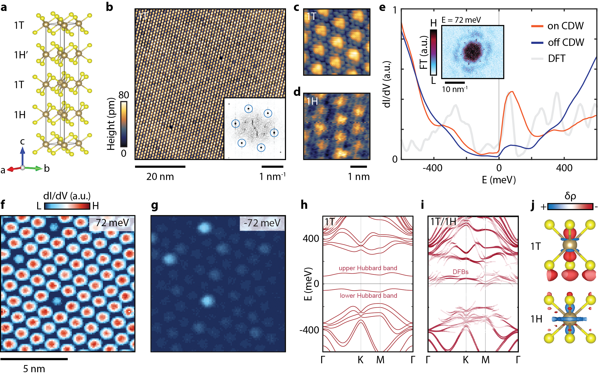
To that end we study the transition metal dichalcogenide (TMD) 4Hb-TaS2, which consists of alternating layers of 1T-TaS2 and 1H-TaS2. A monolayer of 1T-TaS2 is a prototypical Mott insulator and a candidate quantum spin liquid [13, 14, 15]. It hosts a triangular charge density wave (CDW) order under which clusters of 13 Ta atoms reconstruct in a star of David arrangement. This leads to the hybridization of 12 electronic states leaving a single unpaired electronic state per CDW site. Those unpaired states are believed to exhibit large onsite interaction, , compared to their hopping amplitudes and hence form a Mott insulator. Accordingly, the typical density of states (DOS) spectrum in 1T-TaS2 shows an energy gap of about 400 meV appearing symmetrically across the Fermi energy. The energy gap is bounded by two DOS peaks, signifying the lower and upper Hubbard bands. This gives rise to charge arrest and arguably to a spin liquid phase [14, 15], as no magnetic order has been identified in pure 1T samples down to the lowest measured temperatures [16]. There are conflicting indications, however, that in its bulk form hybridization of stacked CDW sites on neighboring 1T-TaS2 layers results in the formation of a band insulator rather than a correlated one [17, 18, 19, 20]. 1H-TaS2 is a metal and at low temperatures becomes a strongly spin-orbit coupled Ising superconductor [21]. The combination of 1T and 1H polytypes thus provides a rich playground to explore strongly correlated effects [11, 22]. This opportunity is readily available in single crystals of 4Hb-TaS2, whose crystal structure is shown in Fig.1a.
In the hybrid compound both the superconducting and the Mott states are profoundly altered. The 4Hb-TaS2 superconductivity was shown to onset concurrently with an increase in Muon spin relaxation [23], suggesting a chiral superconducting phase. More recent STM studies, visualized the existence of topological nodal superconductivity on the 1H surface termination of single crystals [24] possibly akin to similar observations in MBE grown 1H monolayers [25]. The fate of the Mott insulating state on the 1T layers has thus far remained ambiguous. Spectroscopic STM measurements on 4Hb-TaS2 single crystals have found that inter-layer hybridization results in shifting the Hubbard bands to above the Fermi energy [53]. In contrast, the dI/dV spectrum of MBE grown 1T/1H bilayers exhibits clear signatures of Kondo behaviour [27, 28] due to the screening of the localized spins on the CDW sites by the metallic 1H layer underneath [11], possibly constituting a Kondo lattice. A uniform Kondo lattice was also induced and manipulated by intercalating single crystals with Pb atoms [29].
Yet here, we report that both ground states - the Kondo states and the flat band - not only coexist in the 4Hb-TaS2 sample but can even be reversibly switched on demand through a discontinuous transition. On the majority of the CDW sites we observe the upward shift of the Hubbard bands in energy. We show in calculation that this is accompanied by a charge transfer from the 1T to the 1H layers, leading to the formation of a depleted doubly degenerate flat band (FB) above the Fermi energy. Yet, on about 12% of the CDW sites, charge transfer is prevented and the spectrum exhibits a sharp Kondo-like resonance. This results in a residual cluster of Kondo sites embedded among the surrounding flat band state. We show that this Kondo cluster state undergoes a reversible first-order quantum phase transition into the flat band state by variation of temperature and electric field as well as with the aid of the STM tip. We characterize the two ground states, the quantum phase transition that separates them and its evolution across the temperature, electric field and tip-sample interaction axes of the emergent electronic phase diagram. Below, we first characterize the two distinct ground states as they appear in the sample and then demonstrate the induced phase transition among them and investigate its thermodynamic quantum nature.
Results
Depleted Mott versus Kondo states
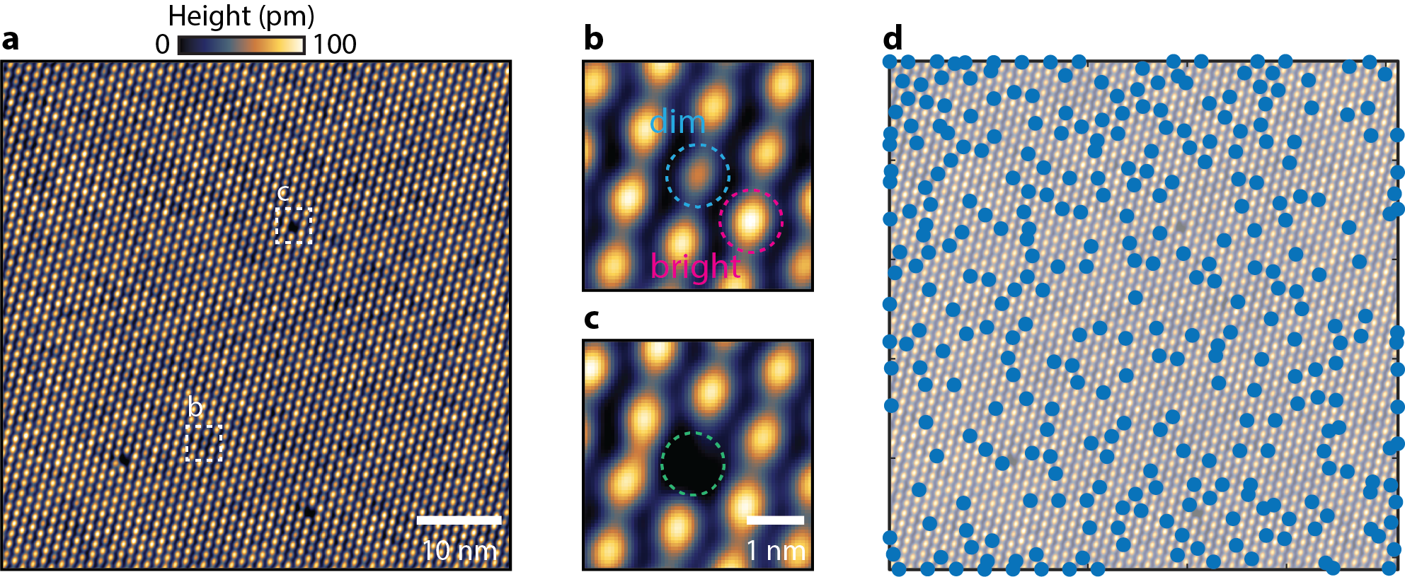
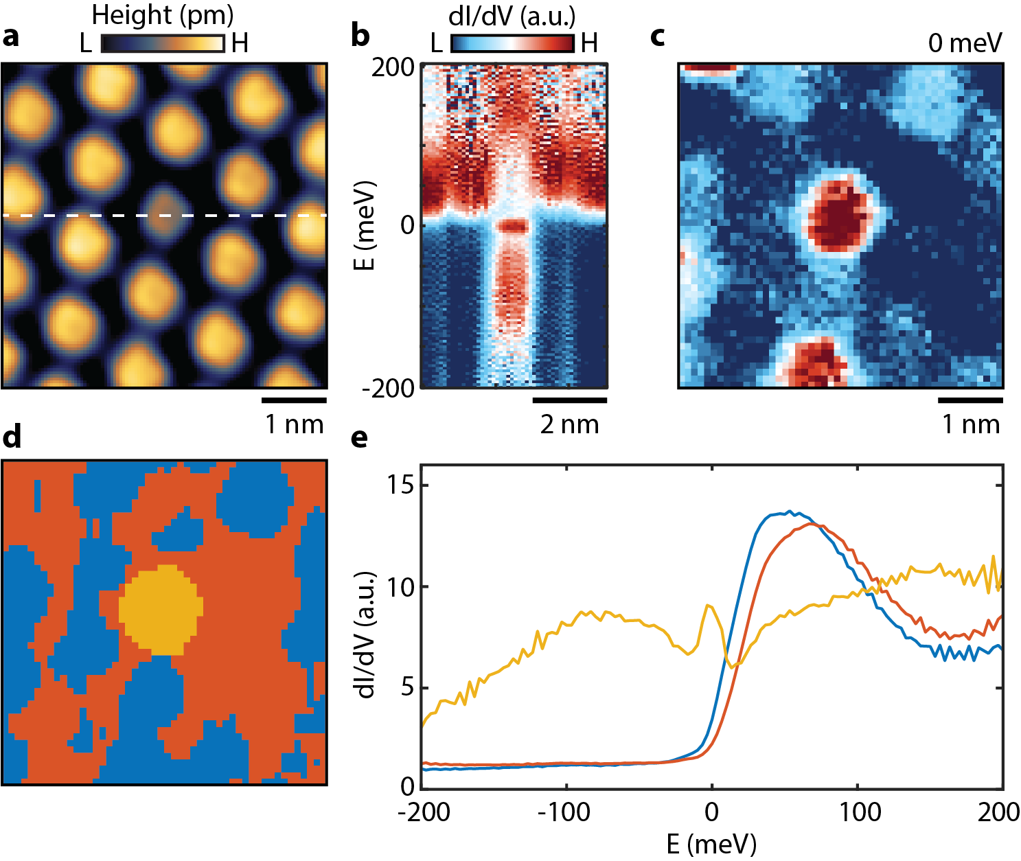
Large single crystals of 4Hb-TaS2 were grown with 1% selenium added to the mixture (see Methods). They were mechanically cleaved at room temperature in ultra-high vacuum conditions and cooled down immediately in a commercial Unisoku STM. The cleaving process randomly exposes distinct 1T and 1H surface terminations. A typical large-scale topography of the 1T layer termination is displayed in Fig. 1b. It shows a commensurate CDW pattern [30, 31] at K. The CDW pattern forms a triangular super-lattice as captured by the Fourier transformed topography (inset). The star of David arrangement, composed of 13 atoms, is clearly seen in the atomically resolved topography in Fig.1c (more details in SM section S1). Intriguingly, in the 4Hb-TaS2 polytype the CDW pattern characteristic to the 1T layer is embedded also onto the adjacent 1H-TaS2 layer (Fig.1d), indicating the mutual interaction between the two layers.
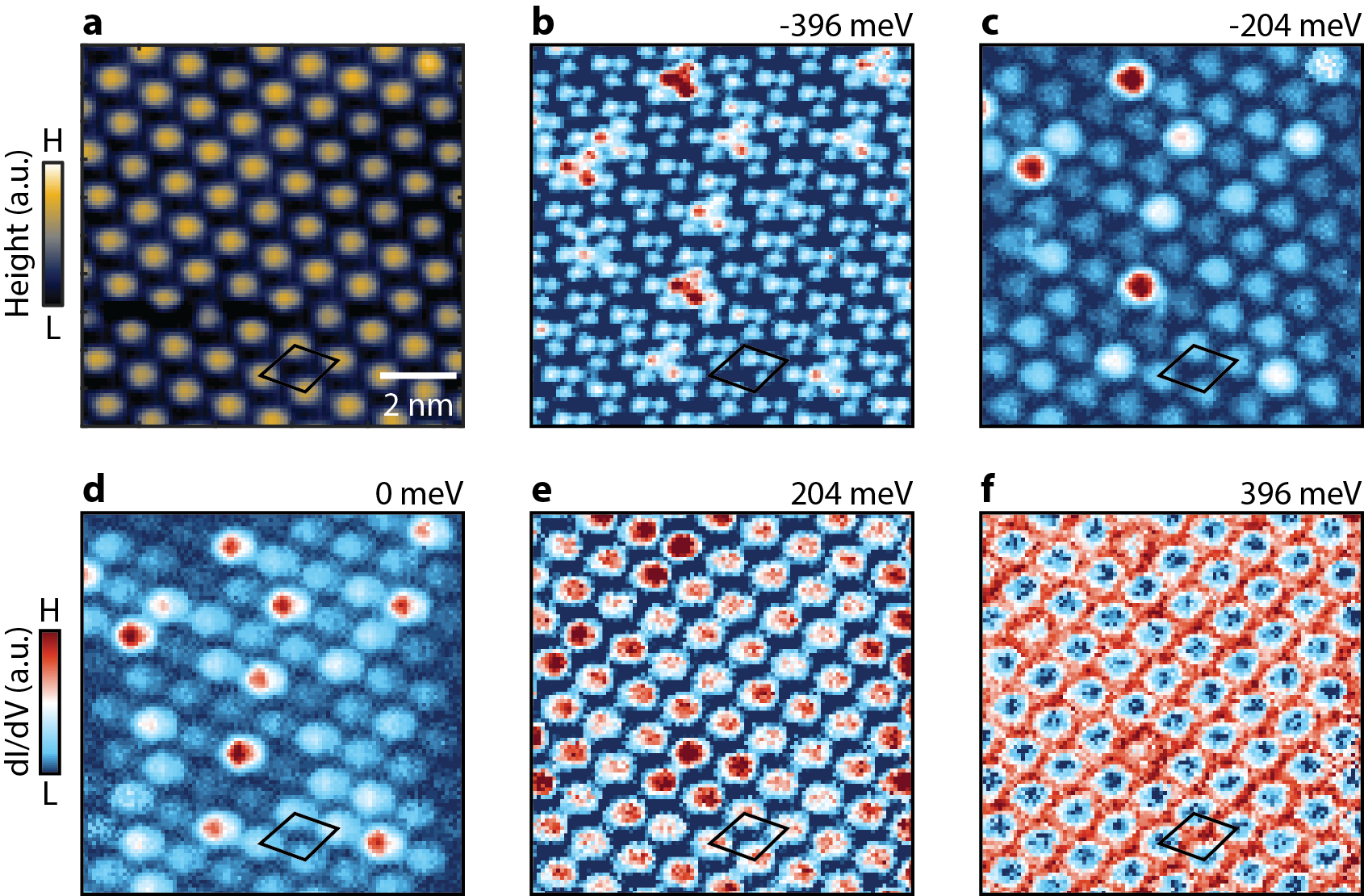
The differential conductance (dI/dV) spectrum of topmost 1T-layers of 4Hb-TaS2 samples look markedly different from the electron-hole symmetric Mott gap seen in pure 1T-TaS2 [32, 33, 34, 20, 35]. Instead, the common on-CDW dI/dV spectrum (Fig.1e, orange) displays an electron-hole asymmetric single pronounced peak that onsets sharply above the Fermi energy and reaches a maximum at about 75 meV. The DOS averaged over the network region, in between CDW sites (blue line), is highly suppressed signifying that the charge distribution remains fairly localized on the CDW sites. The spatial distribution of the DOS and its electron-hole asymmetry above and below the Fermi energy, are mapped in Fig.1f and g, respectively (the three distinct CDW sites that appear dim at positive bias and bright at negative bias will be discussed below).
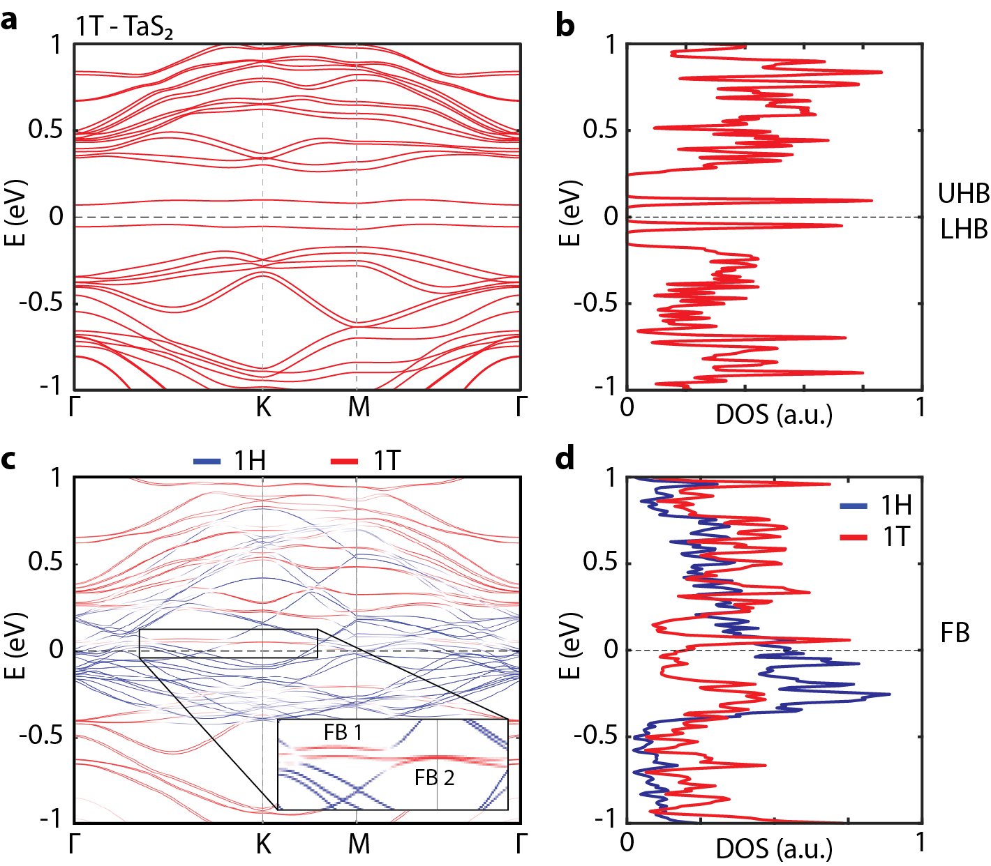
We performed ab initio calculations to resolve the exact origin of the spectrum we observe on the CDW sites. We model a 4Hb-TaS2 bilayer and compare it with the band structure of a 1T-TaS2 monolayer. In the parent 1T-layer, shown in Fig.1h, one finds the known half-filled Mott spectrum hosting two flat Hubbard bands residing symmetrically above and below the Fermi energy (more details in section S2). Upon introduction of an adjacent 1H-layer, the lower Hubbard band gets depleted and shifts in energy to above the Fermi level, giving rise to a pair of fully-depleted flat bands that reside above the Fermi energy. This is displayed in Fig.1i that shows the weight of the 1T/1H bilayer DOS projected on the 1T layer (the complementary projection to the 1H layer is in Fig.S2c). The corresponding integrated DOS shows a sharp peak above the Fermi energy that agrees with the peaked spectrum we measure on the 1T layer (Fig.1e, gray and orange lines, respectively).
This charge depletion from the lower Hubbard band associated with the 1T layer is achieved by charge transfer from the 1T layer to the metallic 1H-layer [36], as shown in Fig.1j. This charge transfer to the 1H layer is evidenced by the 1T characteristic charge modulation that we commonly observe on the 1H layer (Fig.1d). Intriguingly, the quasi-particle interference (QPI) pattern within the energy window of the flat bands (Fig.1e, inset, and in section S3) is symmetric about the CDW Bragg peaks, rather than the atomic ones, signifying the folding of the electronic wavefunction by the CDW superlattice. The measured signature of flat bands agree with previous measurements on single crystal 4Hb-TaS2 [53], but is markedly different from the Kondo spectrum found in artificial 1T/1H bilayers grown via MBE [27, 28] that we discuss next.
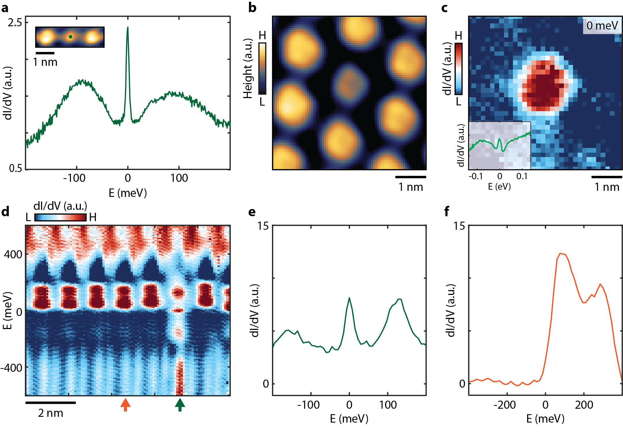
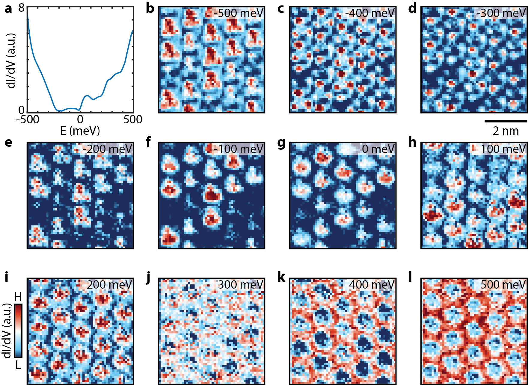
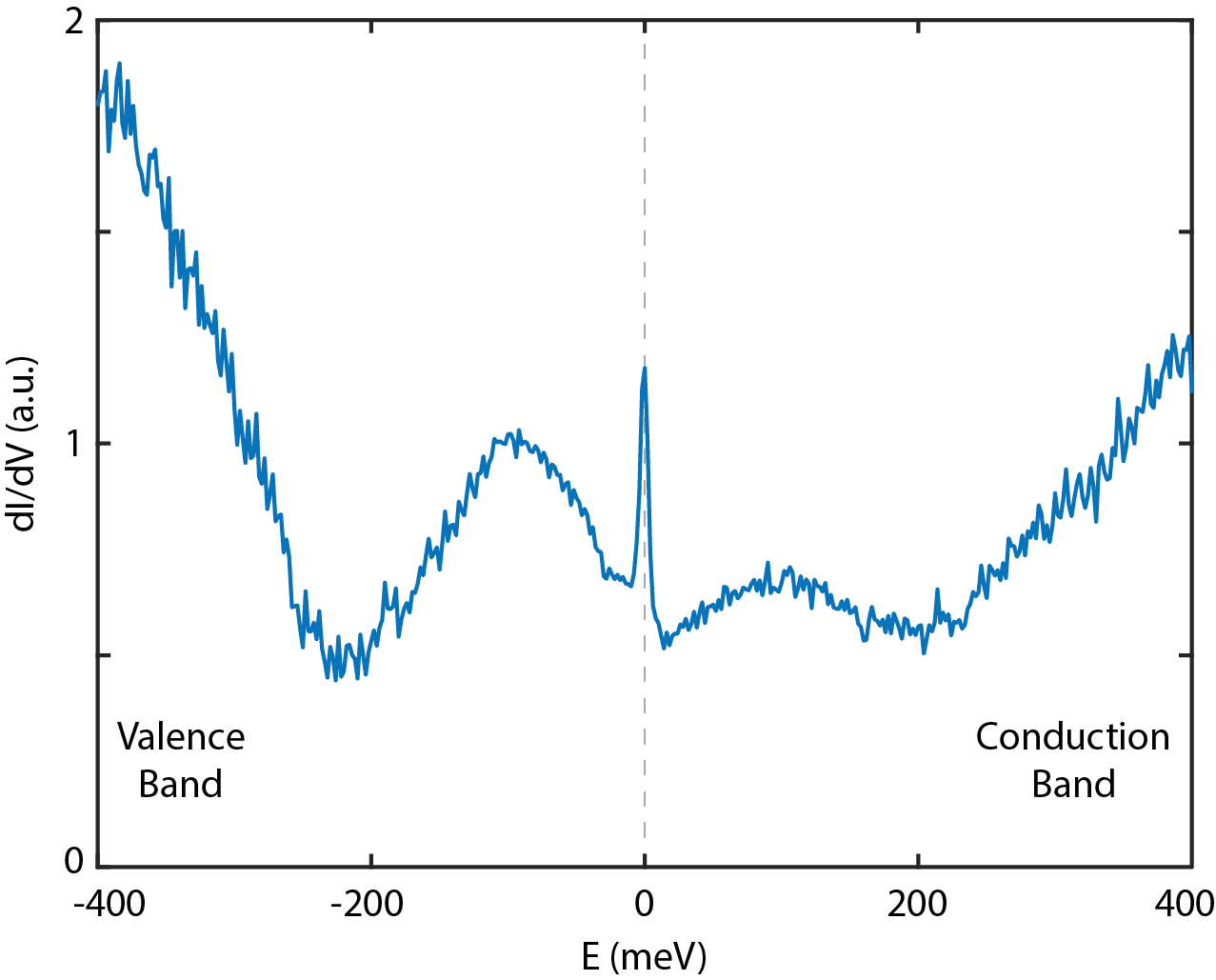
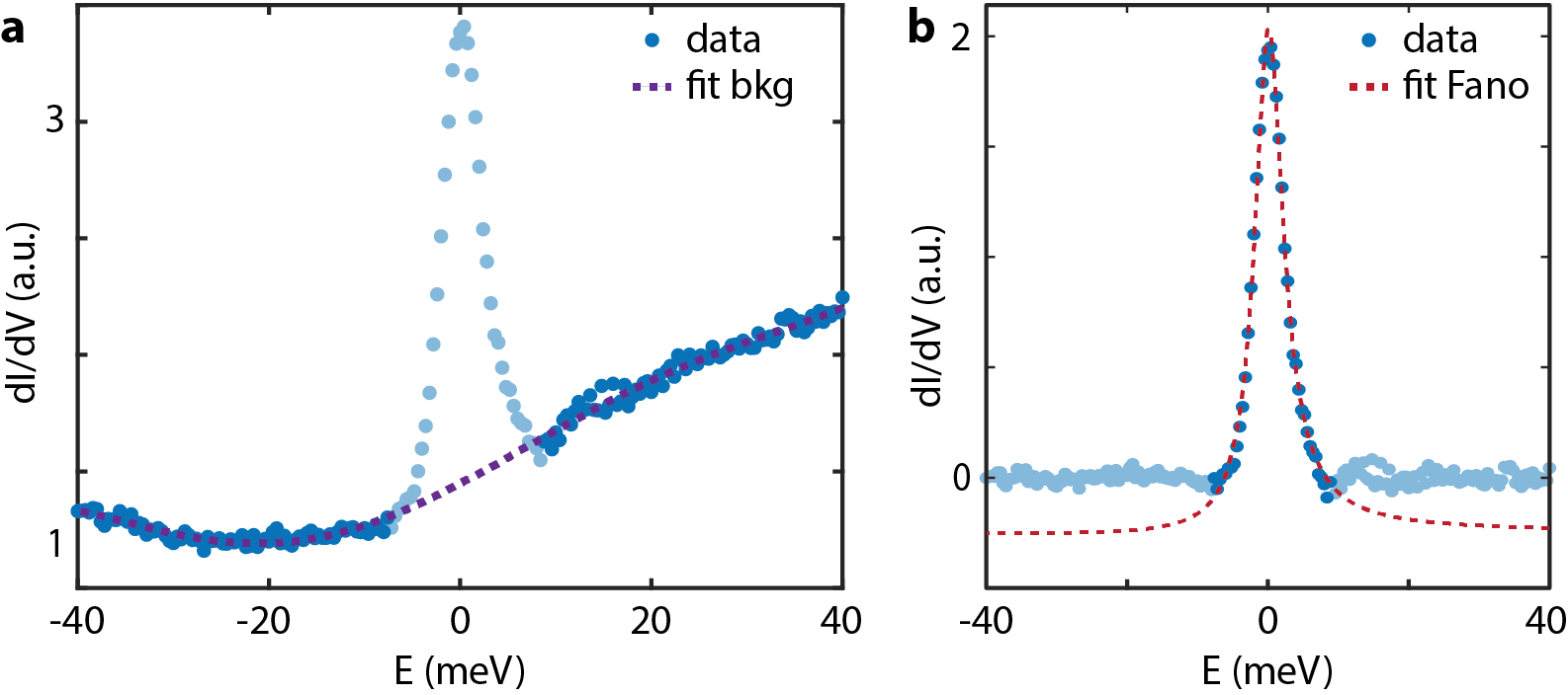
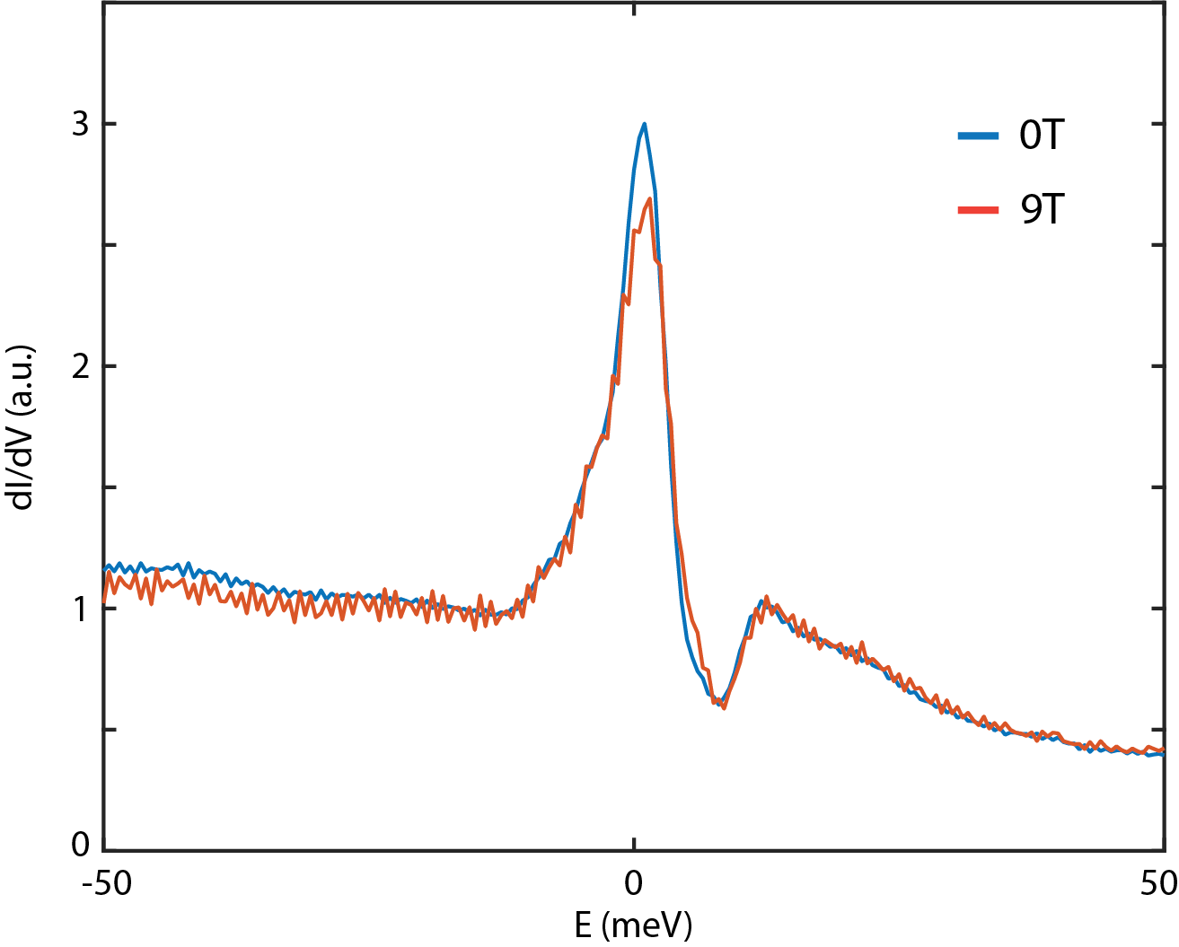
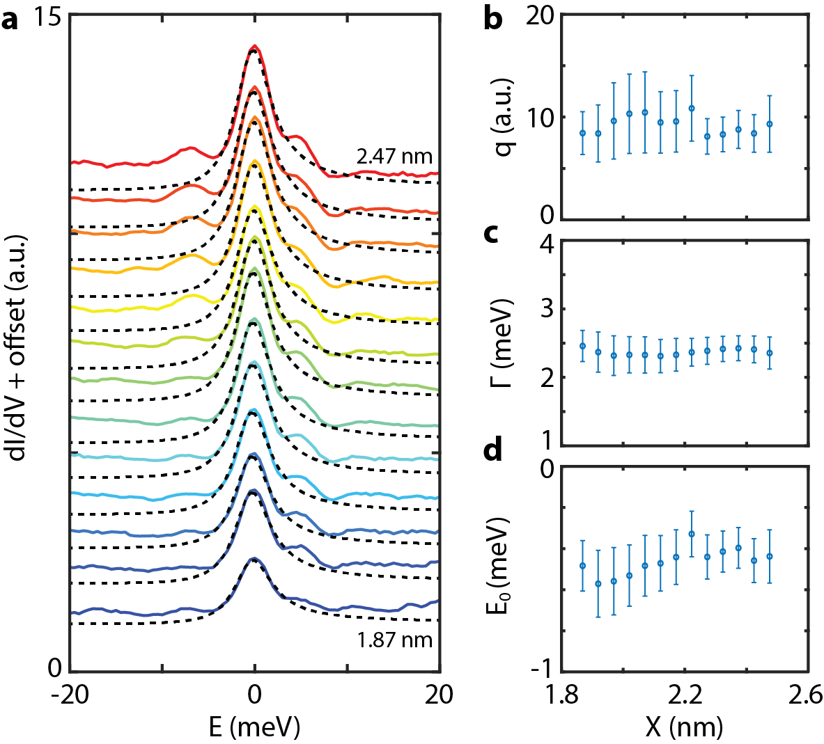
We now focus on a subset of the CDW sites that appear dim (shallower) in positive bias topography as shown in Fig.1b. Those dim sites constitute about 12% of all CDW sites (see SM S4). Their shallow appearance is not topographic but rather rooted in their electronic spectrum. While their exact chemical origin is still uncertain, it may be related to incorporation of Se that was added to the mixture. The local DOS spectrum characteristic of such dim CDW sites is shown in Fig.2a (see also Fig.S8). It displays a sharp zero bias conductance peak (ZBCP) in agreement with recent visualization of a Kondo response in MBE grown 1T/1H bilayers [28, 27]. There, however, it appeared uniform across all CDW sites, while our single crystals mostly host the flat band states and the Kondo spectrum appears only on a subset of sites forming a rather dense cluster. The width of the ZBCP, that reflects the width of the coupling to the metal, is on the order of a few meV (see Fig.S9) and somewhat varies between dim sites. The satellite peaks correspond to charge excitationswhose energy spacing, meV, captures the onsite repulsion and their width, meV, represents the coupling strength to nearby sites or to the metal. The ratio of the two scales, 1, puts those Kondo state close to the intriguing critical regime. We find no response of the Kondo spectrum to application of the maximal magnetic field of 9 T that we can reach (see Fig.S10). While this is quite atypical to isolated Kondo impurities [37], such robustness is rather common in Kondo lattices. In particular, it is consistent with observations made in the MBE grown 4Hb-TaS2 bilayers that host a regular Kondo lattice and showed splitting of the Kondo ZBCP only above a field of 10 T [27]. This suggests that the Kondo cluster that forms in our samples already exhibits Kondo lattice-like correlations.
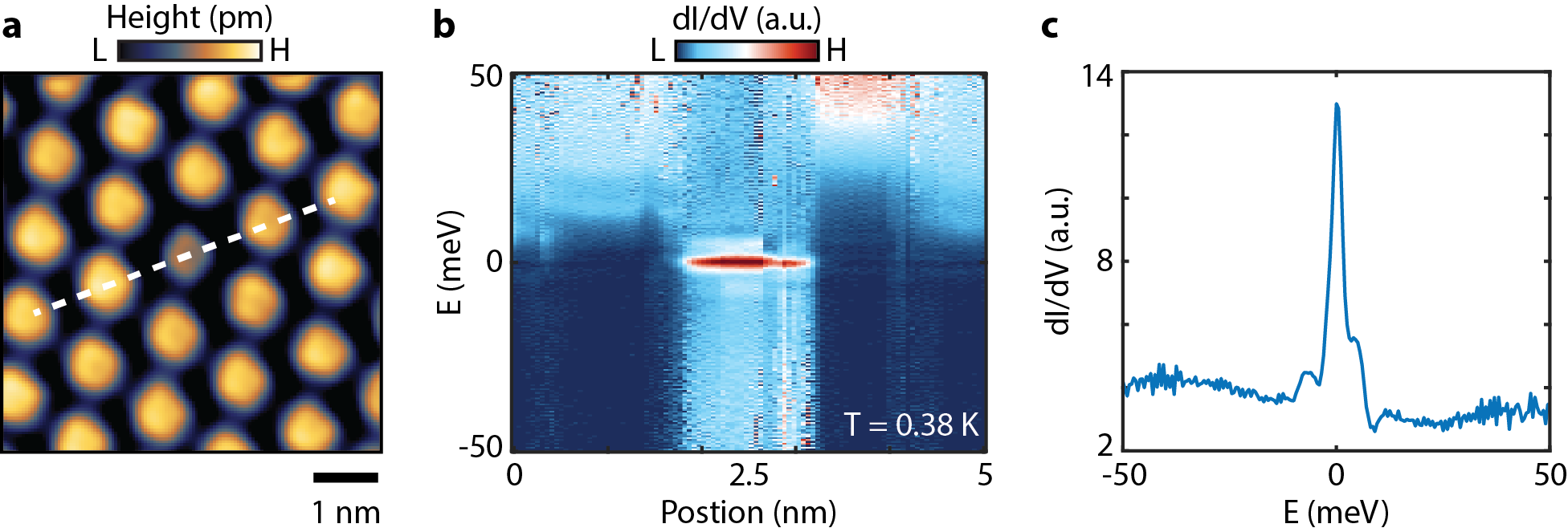
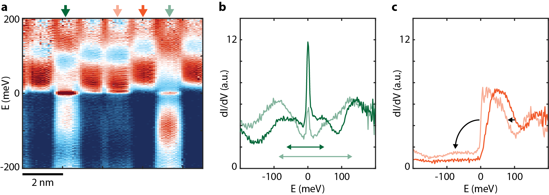
Spatial spectroscopic mapping over the topography shown in Fig.2b of a similar dim CDW site positioned at its center, given in Fig.2c, shows that the ZBCP (full spectrum shown in inset) is distributed across the dim CDW site rather than localized over a single atomic defect (see also section S8). Spatial mapping of the spectrum along a row of CDW sites, shown in Fig.2d (more in Fig.S11), shows the stark distinction between the symmetric Kondo spectrum with satellite peaks on a single dim site to the asymmetric depleted flat band (DFB) state we find on all neighboring sites (spectra shown explicitly in Fig.2e and f, respectively). Intriguingly, CDW sites adjacent to the dim one seem to be somewhat affected as their local spectrum slightly shifts in energy (see also S12) suggesting that the local dim site potential has a long range effect.
First order quantum phase transition in the voltage-temperature phase diagram
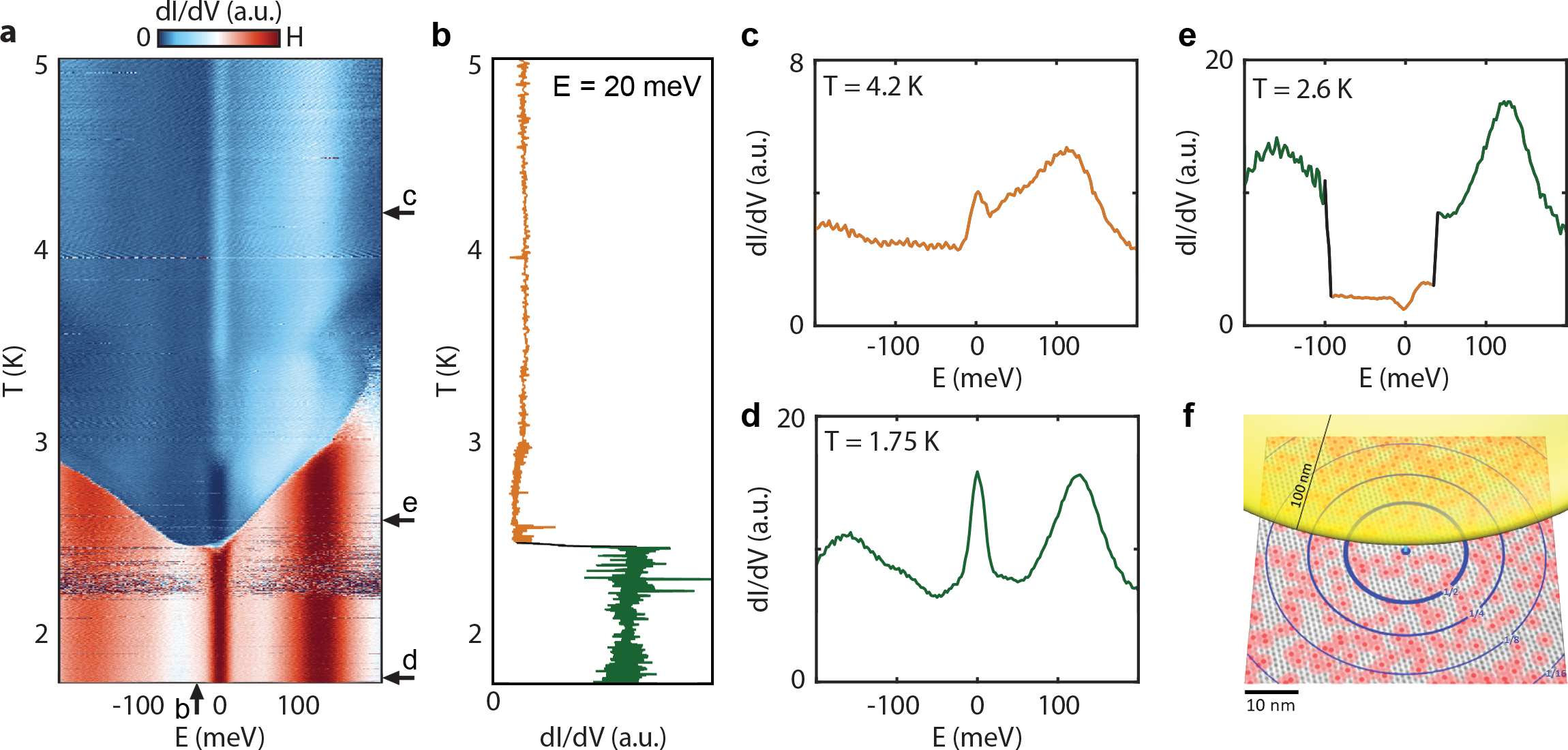
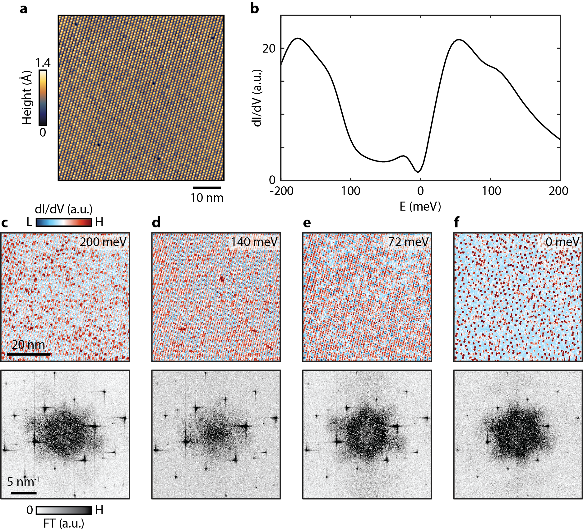
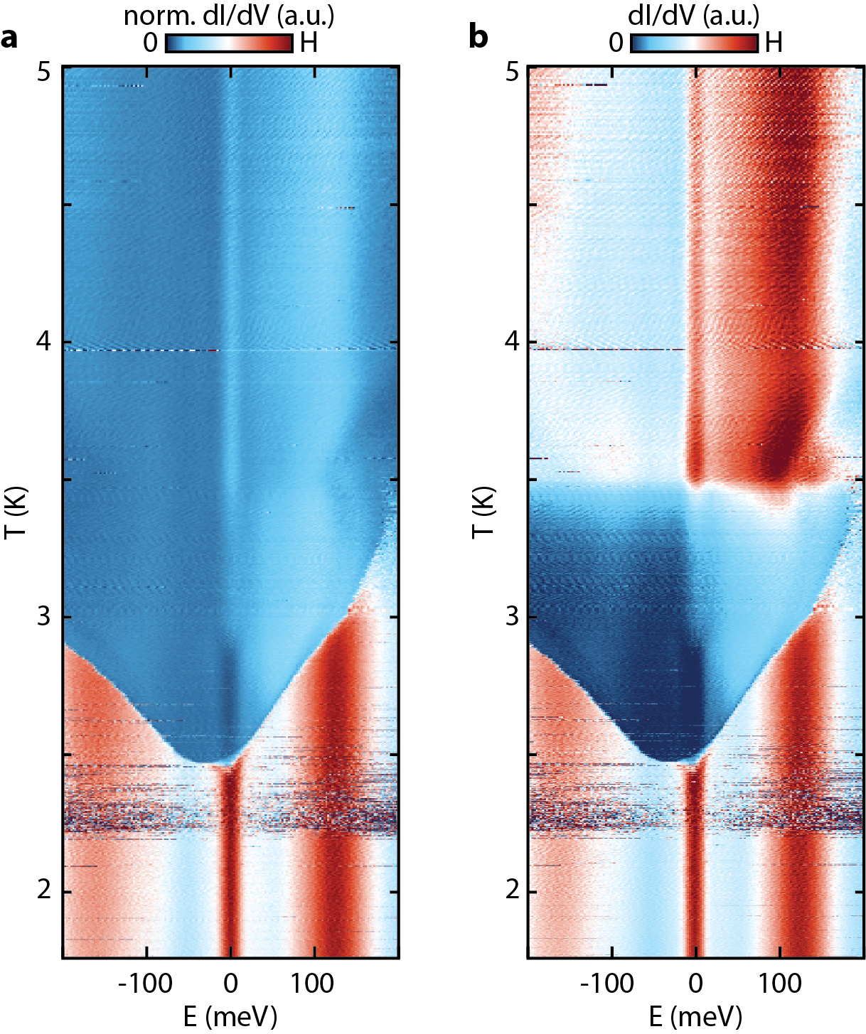
So far all the spectroscopic imaging was conducted at a fixed temperature. Next, we follow the evolution of the dI/dV spectrum on a dim CDW site with varying temperature and electric field and show that it undergoes an abrupt transition from a Kondo state into a flat band state. In Fig.3a we show the dI/dV spectrum measured while gradually raising the temperature. Remarkably, the electron-hole symmetric Kondo spectrum we measure at low temperatures switches to the electron-hole asymmetric flat band spectrum as the temperature is increased. A cut across temperature at a certain applied bias (marked by arrow) is shown in Fig.3b demonstrating the discontinuous character of the transition. At high temperatures, above 3 K, we find the electron-hole asymmetric spectrum of the flat band as shown in Fig.3c. At low temperatures, below 2.5 K, the electron-hole symmetric Kondo spectrum takes over, as shown in Fig.3d. The abrupt jump in the local DOS traced across temperature and electric field thus distinguishes the different electronic spectra of the different electronic ground states. It thus signifies a quantum phase transition line between the Kondo state, observed on dim sites and the flat band ground state associated with the bright sites.
As the mapping in Fig.3a shows the transition is not driven by temperature alone but by its combination with electric field. The latter is applied by the STM tip as the bias voltage is scanned. Indeed, voltage bias scans taken at a fixed temperature within the intermediate range of 2.5-3 K show two sharp discontinuous steps in dI/dV, occurring at positive and negative bias as demonstrated in Fig.3e. These sharp steps in dI/dV that gradually shift towards zero bias with decreasing temperatures both signify the transition from a Kondo state at high negative and positive bias to the flat band state at lower bias. The observation of a sharp transition between distinct dI/dV spectra whose associated temperature varies with applied electric field is remarkable. We could only resolve the evolution of the energy scale at which it occurs from 0 to 200 meV over a temperature window of 0.5 K across which the transition remains perfectly abrupt within the framework of a phase transition. Not all dim CDW sites exhibit such temperature-field driven transition among the parameter spaces we covered. Nevertheless, the occurrence of the phase transition on a subset of the sites allows us to uniquely investigate the nature of the quantum phase transition and its evolution across the mapped phase diagram.
We stress, that unlike the tip to sample tunneling that decays exponentially over a length scale of picometers the electric field the tip imparts is quasi-local as it decays as a power-law. Accordingly, the extended geometry of the STM tip, with a typical radius of curvature of 100 nm (sketched to scale in Fig.3f) should be considered [38]. The blue circles in Fig.3f mark radii at which the electric field between a half-sphere and a plane decays by consecutive multiples of 2 from its peak intensity at the center. It thus becomes evident that while we probe with tunneling the site immediately under the tip, its electrostatic coupling to the sample extends over hundreds of CDW sites.
We use the transition line to further characterize the thermodynamic nature of the first-order quantum phase transition and the competing energy scales involved in it. The transition line appears fairly symmetric across positive and negative bias in the mapped bias-temperature phase diagram. As discussed above, ab initio calculation suggests that the transition involves charge transfer between the localized 1T CDW sites and the 1H metal. This varies the strength of the electric dipole, , between the charge and the STM tip. The coupling energy of the electric field imparted by the STM tip, , to that dipole, , contributes to the free energy of the system and could have driven charge transfer. However, the linear coupling of the electric field to that electric dipole cannot account for the quadratic shape of the transition line seen in Fig.3a. This suggests that the phase transition is driven by the charging energy which is quadratic in the bias voltage, . Since the geometric capacitance is essentially fixed by the shape of the tip and the underlying metallic layer, the transition is rather driven by the contribution to the energy that arises from the difference in the local copmpressibility between the electronic phases on either side of the transition line. These energetic considerations compete with the entropic ones, , where corresponds to the phases on either side of the transition. The thermodynamic first order transition occurs at a voltage dependent temperature, , obtained from . Therefore, we conclude that the Kondo state that appears at lower temperatures is favored due to its higher compressibility relative to the flat band state that is favored by entropy at higher temperatures.
The higher compressibility of the Kondo spectrum naturally arises from the metallic ZBCP compared to the insulating depleted flat bands. The origin of excess entropy of the flat bands at high-temperature is more elusive. Most electronic phase transitions show exactly the opposite behavior: typically low-temperature phases have a reduced instead of an enhanced DOS at the Fermi energy. Thermodynamically, the high-temperature phase has to have a higher entropy compared to the low-temperature phase, while our spectroscopy of the depleted band reveals that the excess entropy cannot arise from electronic excitations in the top 1T layer. Most likely, the excess entropy therefore has its origin in fluctuating spin or charge degrees of freedom which arise when charge is transferred from the 1T to the 1H layer and the detailed nature of the hybridized state that forms as a result of it. It could also arise from the exact character of the microscopic origin of the dim sites, that we could not resolve with certainty.
Though subdominant relative to the compresibility, the charge transfer associated with the phase transition still induces an electric polarization which is reflected in the slight offset of the minimum of the quadratic transition line from zero bias. However, the small value we obtain for the offset of about 25 meV signifies that either the polarization is far smaller than what geometrical considerations suggest or that it is balanced off by a large entropy gain of (see section S14). The origin for the screening of the dipole or excess entropy is yet unresolved though in part it could be related to the relative orientation of the dipole and local electric field that enter the free energy as a vector product. Again, they may also arise from the detailed nature of the defect sites or the hybridized state that they form with the 1H metal that require further investigation.
Tip-induced quantum phase transition
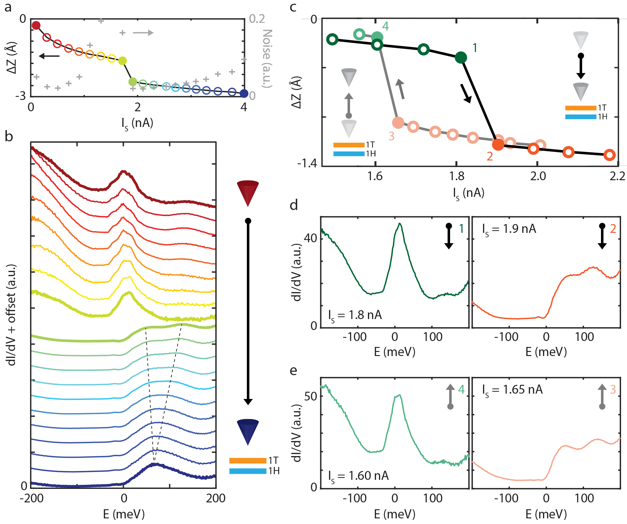
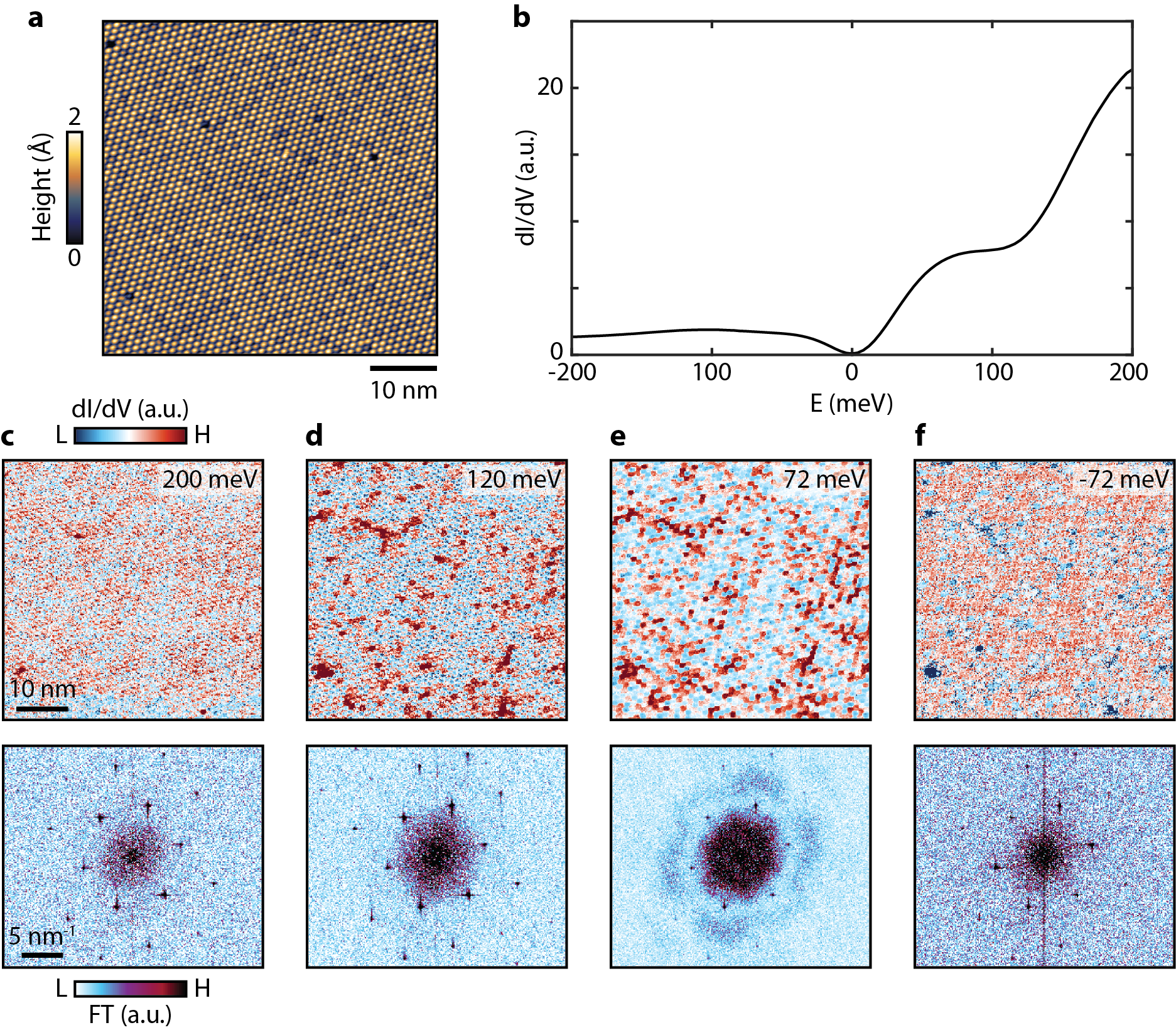
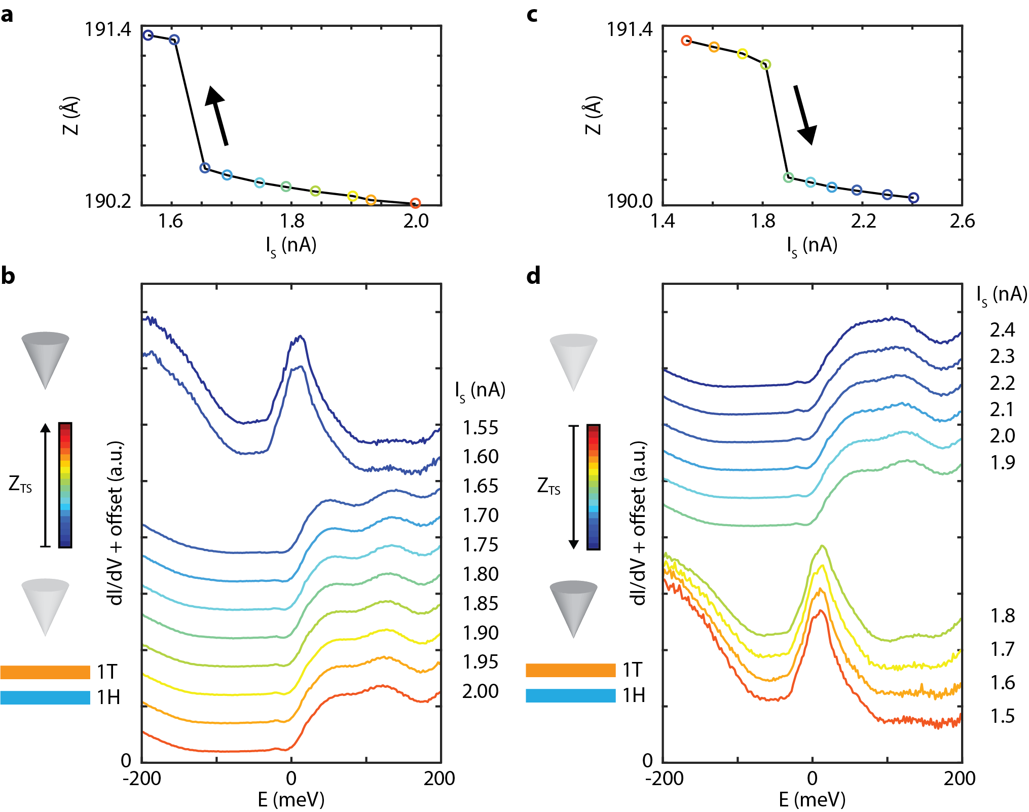
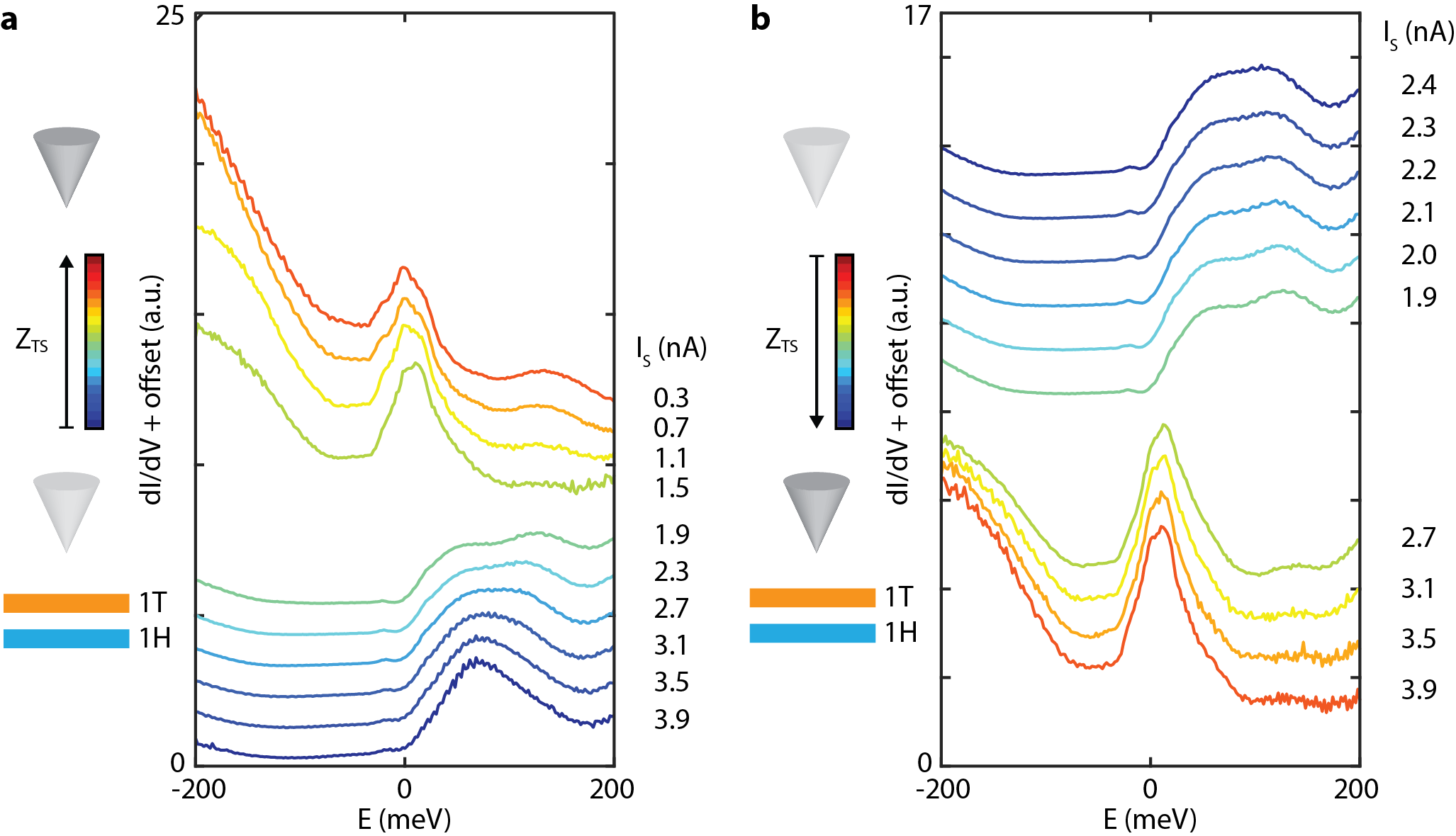
We next show that the quantum phase transition can be induced also by modifying the 1T-1H interlayer coupling via tuning of the distance between the sample and the STM tip and use it to further characterize its nature. In the temperature-bias scans we have discussed above the tip was used as a local electrode [39, 40, 41, 38]. Other than that, tip invasiveness did not play a role in inducing the transition as the tip position was kept mostly fixed (one exception happens when the phase transition line crosses the parking bias as discussed in section S19). More generally though, the STM tip may have different functionalities besides enabling spectroscopic imaging. For instance, it may provides an extra screening channel thus modifying local Coulomb potentials and it may interact with the sample via inter-atomic forces that may alter the inter-layer coupling of layered materials [42, 43]. We show that on certain dim sites the tip’s invasiveness too induces the reversible quantum phase transition between the Kondo and flat band states. the STM tip height above the sample is set not only by the surface topography but also by the integrated DOS from the Fermi energy up to the set bias voltage.
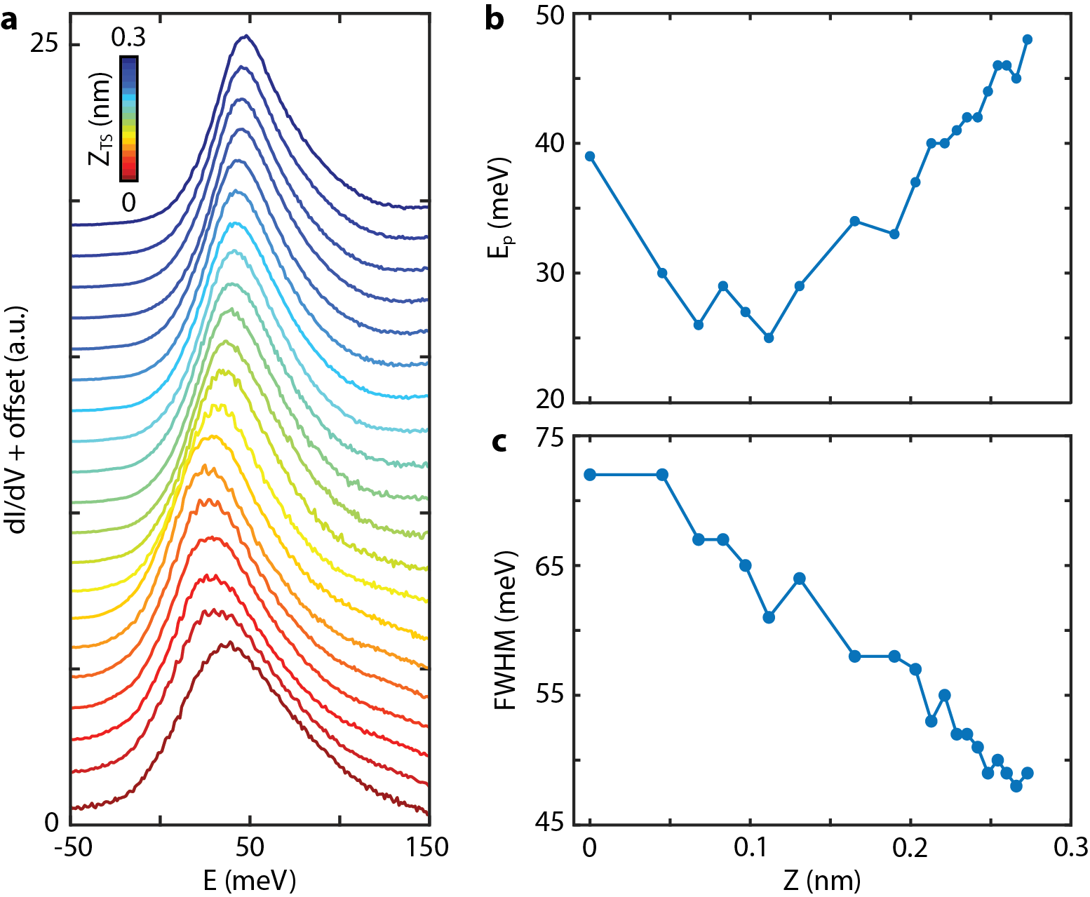
We position the tip at a certain height (on the order of a nanometer) above a dim CDW site by stabilizing a tunneling current, 0.2 nA, under a chosen bias voltage, 200 meV (corresponding to the solid red circle in Fig.4a). The spectrum measured at this initial height shows a Kondo type spectrum hosting a ZBCP (thick red line in Fig.4b) already at 4.2 K - indeed, we find variability at the local conditions at which the transition occours that we attribute to inhomogeneity. We then bring the tip closer to the sample by increasing the set current in steps of (Fig.4a) and monitor the evolving spectrum as the tip approaches the dim CDW site (Fig.4b). Over the initial approach of about 1.5 Angstroms we find no change in the Kondo spectrum. Then, over a single additional step of the spectrum switches abruptly from the symmetric Kondo-type to the asymmetric flat band type. The changing spectrum results in a slightly larger tip height repositioning step over the otherwise exponential background (Fig.4a). We use it as a convenient proxy for identifying the point of transition as it reflects a corresponding change in the spectrum (Fig.4b).
Just past the transition the doubly degenerate flat bands are slightly split in energy, as can be deduced from the double peak structure that characterizes the spectrum. As we continue to approach with the tip further towards the sample the two peaks gradually merge (tracked by dotted lines) into a single peak, resulting in an identical spectrum to the asymmetric degenerate flat band spectrum we commonly find on bright CDW sites (as in Fig.1e). This transition in response to the tip position is similar to the one we have demonstrated above in response to temperature and electric field induced by the tip. Bringing the tip closer amplifies the electric field it induced at a given bias voltage. However, in response to increasing electric field we have induced the opposite transition from a flat band to a Kondo spectrum (see Fig.3e). We thus conclude that the leading effect of bringing the tip closer to the sample is the increasing atomic forces between the two, which in turn affects the coupling between the vand der Waals 1T and 1H layers. Tip invasiveness thus adds a third axis to the temperature-bias phase diagram we have presented above (Fig.3a).
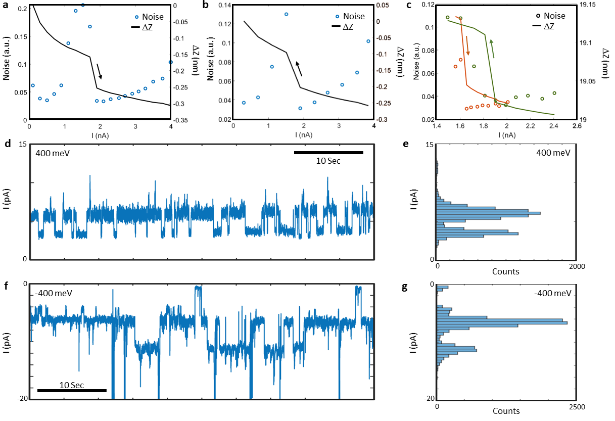
As the transition point is approached we also find a concurrent rise in the noise level of the tunneling dI/dV spectrum. It is seen directly in the individual spectra in Fig.4b and captured by the standard deviation in dI/dV about its mean value shown by plus symbols in Fig.4a. The noise increases sharply on the Kondo branch towards the transition point (regardless of direction of height scan, see section S15) and reduces back upon crossing the transition point. The noise spectrum captured here is of low-frequency with a cutoff of about 1 KHz. Intriguingly, the spectra acquired within the Kondo state appear noisier also in the temperature-bias mappings (see for instance Fig.3b). Seldomly we have also captured telegraphic noise over dim CDW sites with comparable typical switching time-scale of tens of milliseconds up to seconds (Fig.S16) that was absent on bright sites. Such low frequencies are far from being characteristic of single electron processes [44] which are typically on the order of terahertz. This suggests that spatial correlations are present on the Kondo side of the transition that thus involves a larger cluster rather than a single CDW site.
We further examine the sharp transition and its reversibility by taking finer steps about it through the approaching and retracting branches, shown in Fig.4c by dark and light lines, respectively (the corresponding dI/dV spectra are in Fig.S15). Even at such high resolution we still we find that the transition between the Kondo and the flat band spectra occurs abruptly. Remarkably though, the transition height shows a clear hysteresis loop between approaching and retracting branches (Fig.4d and e). These observations too indicate that the Kondo and flat band spectra do not evolve continuously from one to another, but are rather distinguished by a first-order quantum phase transition. It is triggered by the charge transfer back and forth from the 1T-layer to the metallic reservoir of the 1H-layer that can be induced reproducibly by the STM tip (see Fig.S17) as well as by temperature and bias. Not all CDW sites that host Kondo states allow such tip manipulation within the parameter space we have tested. Nevertheless, the sites on which such tunability is realized enable us to uniquely investigate the interplay between the two electronic states. The origin of the hysteresis may involve the tip control as the abrupt change in the spectrum is accompanied with an abrupt repositioning of the tip height. No similar response was detected when repeating such tip approach protocols on bright sites hosting flat band spectrum (see section S18).
Discussion
The appearance of a first order quantum phase transition with such temperature-bias relation who is accompanied by a hysteresis loop and associated low frequency noise does not adhere to the phenomenology of an isolated electronic defect state. The typical time scales of electronic states of matter and specifically switching times of isolated Kondo states are incompatible to those we encounter [45]. The lack of magnetic response of the ZBCP is also characteristic of correlated Kondo sites as in a Kondo lattice [27] rather than isolated Kondo states [37]. Indeed, 12% concentration of dim defect sites translate to dim sites being next nearest neighbors on the average. The connected cluster is demonstrated on top of the topographic image in Fig.3f, where all dim defect sites are marked with a red dot and the distance to their nearest neighbors by light red circle showing the close proximity. On the other hand, the electrostatic coupling of the STM tip to that Knodo cluster extends over hundreds of CDW sites [38] as demonstrated in Fig.3f by concentric circles. The imaged phase transition thus signifies the presence of correlations at least on a mesoscopic scale.
The observations reported here provide a potential exciting pathway for investigating the gradual onset of correlated phases and phase transitions among them. However, to perform this systematically the origin of the Kondo sites has to be clarified. If we assume a dim CDW site is caused by a single atomic defect, their abundance per atom (12% of all CDW sites with 13 atoms in each site) roughly agrees with the 1% selenium to sulfur concentration used during growth for stabilizing the 4Hb polytype of TaS2. Indeed, compared to 1H-TaS2, the work function of 1H-TaSe2 is slightly closer to that of 1T-TaS2. However, quantitatively to prevent charge transfer to occur in ab initio calculation requires substituting all 13 sulfur atoms under a certain CDW site with tellurium rather than selenium atoms, neither of which are realistic. Similarity with recent imaging of Pb intercalated 1T-TaS2 [46] may suggest that selenium is intercalated between the 1T and 1H layers rather than substituted. On the other hand, the phenomenology that we report here seems to be dissimilar to a recent study of Pb intercalation that induced a uniform Kondo lattice that allowed some tunability but did not undergo a phase transition [29]. We have never observed a clear atomic defect nor an adatom on the 1T or 1H layers. If indeed the Kondo site concentration is set by Se concentration in the flux it would be exciting to gradually modify it in future investigations and explore the evolution of the electronic phase diagram and the quantum first-order phase transition it hosts.
Our spectroscopic findings also reflect on previous observations reported on 4Hb-TaS2. The identification of a dense Kondo cluster, where the spin on the 1T layer is screened by the metallic 1H layers, could suggest alternative origin for the enhancement of Muon spin relaxation that was seen to onset once the material turns superconducting [23]. Within the superconducting state Kondo screening is suppressed, thus revealing a stronger magnetic environment for the Muons. More recently, an intriguing vortex memory effect from above the superconducting critical temperature was identified in single crystals of 4Hb-TaS2 [47]. It suggests the existence of a time-reversal symmetry broken phase that lacks magnetization but still facilitates magnetic memory. It was attributed to a chiral spin liquid phase that has been considered to reside on the 1T-TaS2 layers. However, our observations of charge and spin transfer from the majority of CDW sites on the 1T-TaS2 layers to the 1H-TaS2 metal (superconducitng below 2.7 K), alongside the spectroscopic collapse of the Mott spectrum, exclude the formation of a spin liquid phase there. Nevertheless, our identification of a Kondo cluster may provide alternative context for future investigations for the combined ground state, such as a Kondo glassy state, and its effect on the superconducting state at lower temperatures.
Intriguingly, the zero-bias transition temperature of the quantum phase transition we report here coincides with the superconducting transition temperature of bulk 4Hb-TaS2. While this may be a mere coincidence, it can also hint that the low temperature Knodo cluster state is more susceptible to condensation and thus promotes a concurrent superconducting transition [48]. With respect to previous spectroscopic reports of 4Hb-TaS2, our observations here suggest that the mechanism that led MBE grown 1H/1T bilayers to show a uniform Kondo state [27, 28] lies in absence of charge transfer. A plausible reason for that is lack of sufficient commensurate conditions that is required to induce it. In contrast, pure 4Hb-TaS2 single crystals do not host defect states [53] that have allowed us here to induce and manipulate the first-order quantum phase transition that separates the two states.
Figures
Methods
DFT calculations
We performed the density-functional theory (DFT) calculation follows in the framework of the generalized gradient approximation [49]) with the Vienna ab-intio package [50]. We employed the PBE-D2 method to describe vdW interaction [51]. We included spin-orbit coupling (SOC) interaction in all calculations. The 4Hb structure with supercell was used for the CDW reconstructed structure. Full geometry optimization was performed until the Hellmann-Feynmann force acting on each atom became smaller than 0.01 eV/Å.
In the optimized structure, the 1T layer forms the star of David (SD) structure and the 1H layer remains almost the same (less than 1% change). To evaluate interlayer interaction, we evaluated the charge transfer between the 1H and 1T layers. Because the 1T phase has about half eV lower work function than the 2H phase [52], charge may transfer from the 1T layer to the 1H layer when forming an interface. As the result of charge transfer, We indeed observe the decrease (increase) of charge in the 1T (1H) side, resulting a charge dipole at the 1T-1H interface.
Data availability
The data that support the plots within this paper and other findings of this study are available from the corresponding authors upon reasonable request.
References
- [1] Leon Balents, Cory R. Dean, Dmitri K. Efetov and Andrea F. Young “Superconductivity and strong correlations in moiré flat bands” In Nat. Phys. 16 Nature Publishing Group, 2020, pp. 725–733
- [2] Dante M. Kennes, Martin Claassen, Lede Xian, Antoine Georges, Andrew J. Millis, James Hone, Cory R. Dean, D.. Basov, Abhay N. Pasupathy and Angel Rubio “Moiré heterostructures as a condensed-matter quantum simulator” In Nat. Phys. 17 Nature Publishing Group, 2021, pp. 155–163 URL: http://www.nature.com/articles/s41567-020-01154-3
- [3] Masatoshi Imada, Atsushi Fujimori and Yoshinori Tokura “Metal-insulator transitions” In Rev. Mod. Phys. 70.4 American Physical Society, 1998, pp. 1039–1263
- [4] Lucile Savary and Leon Balents “Quantum spin liquids: a review” In Reports Prog. Phys. 80.1 IOP Publishing, 2017, pp. 016502
- [5] C. Broholm, R.. Cava, S.. Kivelson, D.. Nocera, M.. Norman and T. Senthil “Quantum spin liquids” In Science 367.6475 American Association for the Advancement of Science, 2020, pp. eaay0668
- [6] Patrick A. Lee, Naoto Nagaosa and Xiao Gang Wen “Doping a Mott insulator: Physics of high-temperature superconductivity” In Rev. Mod. Phys. 78.1 American Physical Society, 2006, pp. 17
- [7] N. Reyren, S. Thiel, A.. Caviglia, L. Fitting Kourkoutis, G. Hammerl, C. Richter, C.. Schneider, T. Kopp, A.. Rüetschi, D. Jaccard, M. Gabay, D.. Muller, J.. Triscone and J. Mannhart “Superconducting interfaces between insulating oxides” In Science 317.5842 American Association for the Advancement of Science, 2007, pp. 1196–1199
- [8] Changjiang Liu, Xi Yan, Dafei Jin, Yang Ma, Haw Wen Hsiao, Yulin Lin, Terence M. Bretz-Sullivan, Xianjing Zhou, John Pearson, Brandon Fisher, J. Jiang, Wei Han, Jian Min Zuo, Jianguo Wen, Dillon D. Fong, Jirong Sun, Hua Zhou and Anand Bhattacharya “Two-dimensional superconductivity and anisotropic transport at KTaO (111) interfaces” In Science 371.6530 American Association for the Advancement of Science, 2021, pp. 716–721
- [9] Takahiro Misawa, Yusuke Nomura, Silke Biermann and Masatoshi Imada “Self-optimized superconductivity attainable by interlayer phase separation at cuprate interfaces” In Sci. Adv. 2 American Association for the Advancement of Science, 2016
- [10] Lele Ju, Tianshuang Ren, Zhu Li, Zhongran Liu, Chuanyu Shi, Yuan Liu, Siyuan Hong, Jie Wu, He Tian, Yi Zhou and Yanwu Xie “Emergence of high-temperature superconductivity at the interface of two Mott insulators” In Preprint at https://arxiv.org/abs/2111.11662
- [11] R.. Helmes, T.. Costi and A. Rosch “Kondo proximity effect: How does a metal penetrate into a Mott insulator?” In Phys. Rev. Lett. 101.6 American Physical Society, 2008, pp. 066802
- [12] Daniel J. Rizzo, Bjarke S. Jessen, Zhiyuan Sun, Francesco L. Ruta, Jin Zhang, Jia-Qiang Yan, Lede Xian, Alexander S. McLeod, Michael E. Berkowitz, Kenji Watanabe, Takashi Taniguchi, Stephen E. Nagler, David G. Mandrus, Angel Rubio, Michael M. Fogler, Andrew J. Millis, James C. Hone, Cory R. Dean and D.. Basov “Charge-Transfer Plasmon Polaritons at Graphene/-RuCl3 Interfaces” In Nano Lett. 20.12 American Chemical Society, 2020, pp. 8438–8445
- [13] B. Sipos, A.. Kusmartseva, A. Akrap, H. Berger, L. Forró and E. Tutǐ “From Mott state to superconductivity in 1T-TaS2” In Nat. Mater. 7.12 Nature Publishing Group, 2008, pp. 960–965
- [14] K T Law and Patrick A Lee “1T-TaS2 as a quantum spin liquid” In Proc. Natl. Acad. Sci. 114.27 National Academy of Sciences, 2017, pp. 6996–7000
- [15] Yi Chen et al. “Strong correlations and orbital texture in single-layer 1T-TaSe2” In Nat. Phys. 16.2, 2020, pp. 218–224
- [16] A. Ribak, I. Silber, C. Baines, K. Chashka, Z. Y. Dagan and A. Kanigel “Gapless excitations in the ground state of 1T-TaS2” In Phys. Rev. B 96, 2017, pp. 195131
- [17] T. Ritschel, J. Trinckauf, K. Koepernik, B. Büchner, M. Zimmermann, H. Berger, Y.. Joe, P. Abbamonte and J. Geck “Orbital textures and charge density waves in transition metal dichalcogenides” In Nature Physics 11 Nature Publishing Group, 2015, pp. 328–331
- [18] T Ritschel, H Berger and J Geck “Stacking-driven gap formation in layered 1T-TaS2” In Physical Review B 98, 2018, pp. 195134
- [19] Sung Hoon Lee, Jung Suk Goh and Doohee Cho “Origin of the Insulating Phase and First-Order Metal-Insulator Transition in 1T-TaS2” In Physical Review Letters 122 American Physical Society, 2019, pp. 106404
- [20] C.. Butler, M. Yoshida, T. Hanaguri and Y. Iwasa “Mottness versus unit-cell doubling as the driver of the insulating state in 1T-TaS2” In Nat. Comm. 11 Nature Publishing Group, 2020, pp. 1–6
- [21] Sergio C. Barrera, Michael R. Sinko, Devashish P. Gopalan, Nikhil Sivadas, Kyle L. Seyler, Kenji Watanabe, Takashi Taniguchi, Adam W. Tsen, Xiaodong Xu, Di Xiao and Benjamin M. Hunt “Tuning Ising superconductivity with layer and spin–orbit coupling in two-dimensional transition-metal dichalcogenides” In Nat. Commun. 9.1 Nature Publishing Group, 2018, pp. 1427
- [22] K.. Al-Hassanieh, Julián Rincón, G. Alvarez and E. Dagotto “Spin Andreev-like reflection in metal-Mott insulator heterostructures” In Phys. Rev. Lett. 114.6 American Physical Society, 2015, pp. 066401
- [23] A. Ribak, R. Skiff, M. Mograbi, P.. Rout, M.. Fischer, J. Ruhman, K. Chashka, Y. Dagan and A. Kanigel “Chiral superconductivity in the alternate stacking compound 4Hb-TaS2” In Sci. Adv. 6.13, 2020, pp. eaax9480
- [24] Abhay Kumar Nayak, Aviram Steinbok, Yotam Roet, Jahyun Koo, Gilad Margalit, Irena Feldman, Avior Almoalem, Amit Kanigel, Gregory A. Fiete, Binghai Yan, Yuval Oreg, Nurit Avraham and Haim Beidenkopf “Evidence of topological boundary modes with topological nodal-point superconductivity” In Nat. Phys. 17.12 Nature Publishing Group, 2021, pp. 1413–1419
- [25] Viliam Vaňo, Somesh Chandra Ganguli, Mohammad Amini, Linghao Yan, Maryam Khosravian, Guangze Chen, Shawulienu Kezilebieke, Jose L. Lado and Peter Liljeroth “Evidence of nodal f-wave superconductivity in monolayer 1H-TaS2 with hidden order fluctuations” In Preprint at https://arxiv.org/abs/2112.07316v1, 2021
- [26] Chenhaoping Wen, Jingjing Gao, Yuan Xie, Qing Zhang, Pengfei Kong, Jinghui Wang, Yilan Jiang, Xuan Luo, Jun Li, Wenjian Lu, Yu-Ping Sun and Shichao Yan “Revealing the roles of narrow electronic band near Fermi level in 1T-TaS2 related layered materials” In Phys. Rev. Lett. 126.25 American Physical Society, 2021, pp. 256402
- [27] Viliam Vaňo, Mohammad Amini, Somesh Chandra Ganguli, Guangze Chen, Jose L Lado, Shawulienu Kezilebieke and Peter Liljeroth “Artificial heavy fermions in a van der Waals heterostructure” In Nature 599.7886, 2021, pp. 582–586
- [28] Wei Ruan, Yi Chen, Shujie Tang, Jinwoong Hwang, Hsin-Zon Tsai, Ryan L. Lee, Meng Wu, Hyejin Ryu, Salman Kahn, Franklin Liou, Caihong Jia, Andrew Aikawa, Choongyu Hwang, Feng Wang, Yongseong Choi, Steven G Louie, Patrick A Lee, Zhi-Xun Shen, Sung-Kwan Mo and Michael F Crommie “Evidence for quantum spin liquid behaviour in single-layer 1T-TaSe2 from scanning tunnelling microscopy” In Nat. Phys. 17.10, 2021, pp. 1154–1161
- [29] Shiwei Shen, Tian Qin, Jingjing Gao, Chenhaoping Wen, Jinghui Wang, Wei Wang, Jun Li, Xuan Luo, Wenjian Lu, Yuping Sun and Shichao Yan “Coexistence of Quasi-two-dimensional Superconductivity and Tunable Kondo Lattice in a van der Waals Superconductor” In Chin. Phys. Lett. 39 Chinese Physical Society, 2022, pp. 077401 DOI: 10.1088/0256-307X/39/7/077401
- [30] Xian Liang Wu and Charles M. Lieber “Hexagonal domain-like charge density wave phase of TaS2 determined by scanning tunneling microscopy” In Science 243.4899, 1989, pp. 1703–1705
- [31] R.V. Coleman, B. Giambattista, P.K. Hansma, A. Johnson, W.W. McNairy and C.G. Slough “Scanning tunnelling microscopy of charge-density waves in transition metal chalcogenides” In Adv. Phys. 37.6 Taylor & Francis Group, 1988, pp. 559–644
- [32] Liguo Ma, Cun Ye, Yijun Yu, Xiu Fang Lu, Xiaohai Niu, Sejoong Kim, Donglai Feng, David Tománek, Young-Woo Son, Xian Hui Chen and Yuanbo Zhang “A metallic mosaic phase and the origin of Mott-insulating state in 1T-TaS2” In Nat. Comm. 7 Nature Publishing Group, 2016, pp. 10956
- [33] Doohee Cho, Sangmo Cheon, Ki Seok Kim, Sung Hoon Lee, Yong Heum Cho, Sang Wook Cheong and Han Woong Yeom “Nanoscale manipulation of the Mott insulating state coupled to charge order in 1T-TaS2” In Nat. Comm. 7 Nature Publishing Group, 2016, pp. 1–6
- [34] Shuang Qiao, Xintong Li, Naizhou Wang, Wei Ruan, Cun Ye, Peng Cai, Zhenqi Hao, Hong Yao, Xianhui Chen, Jian Wu, Yayu Wang and Zheng Liu “Mottness collapse in 1T-TaS2-xSex transition-metal dichalcogenide: An interplay between localized and itinerant orbitals” In Phys. Rev. X 7.4 American Physical Society, 2017, pp. 041054
- [35] C.. Butler, M. Yoshida, T. Hanaguri and Y. Iwasa “Doublonlike Excitations and Their Phononic Coupling in a Mott Charge-Density-Wave System” In Phys. Rev. X 11 American Physical Society, 2021, pp. 011059
- [36] Ziying Wang, Yi Yang Sun, Ibrahim Abdelwahab, Liang Cao, Wei Yu, Huanxin Ju, Junfa Zhu, Wei Fu, Leiqiang Chu, Hai Xu and Kian Ping Loh “Surface-Limited Superconducting Phase Transition on 1T-TaS2” In ACS Nano 12.12 American Chemical Society, 2018, pp. 12619–12628
- [37] A. Otte, Ternes and K. al. M. Bergmann “ The role of magnetic anisotropy in the Kondo effect” In Nat. Phys. 4, 2008, pp. 847
- [38] Alexander Kerelsky, Carmen Rubio-Verdú, Lede Xian, Dante M. Kennes, Dorri Halbertal, Nathan Finney, Larry Song, Simon Turkel, Lei Wang, Kenji Watanabe, Takashi Taniguchi, James Hone, Cory Dean, Dmitri N. Basov, Angel Rubio and Abhay N. Pasupathy “Moiréless correlations in ABCA graphene” In PNAS 118, 2021, pp. e2017366118
- [39] R Dombrowski, Chr Steinebach, Chr Wittneven, M Morgenstern and R Wiesendanger “Tip-induced band bending by scanning tunneling spectroscopy of the states of the tip-induced quantum dot on InAs(110)” In Phys. Rev. B 59.12, 1999, pp. 8043–8048
- [40] Yue Zhao, Jonathan Wyrick, Fabian D. Natterer, Joaquin F. Rodriguez-Nieva, Cyprian Lewandowski, Kenji Watanabe, Takashi Taniguchi, Leonid S. Levitov, Nikolai B. Zhitenev and Joseph A. Stroscio “Creating and probing electron whispering-gallery modes in graphene” In Science 348.6235 American Association for the Advancement of Science, 2015, pp. 672–675
- [41] James L. Collins, Anton Tadich, Weikang Wu, Lidia C. Gomes, Joao N.. Rodrigues, Chang Liu, Jack Hellerstedt, Hyejin Ryu, Shujie Tang, Sung-Kwan Mo, Shaffique Adam, Shengyuan A. Yang, Michael S. Fuhrer and Mark T. Edmonds “Electric-field-tuned topological phase transition in ultrathin Na3Bi” In Nature 564.7736 Nature Publishing Group, 2018, pp. 390–394
- [42] Matthew Yankowitz, K. Watanabe, T. Taniguchi, Pablo San-Jose and Brian J. LeRoy “Pressure-induced commensurate stacking of graphene on boron nitride” In Nat. Commun. 7.1 Nature Publishing Group, 2016, pp. 13168
- [43] Alexander Georgi, Peter Nemes-Incze, Ramon Carrillo-Bastos, Daiara Faria, Silvia Viola Kusminskiy, Dawei Zhai, Martin Schneider, Dinesh Subramaniam, Torge Mashoff, Nils M. Freitag, Marcus Liebmann, Marco Pratzer, Ludger Wirtz, Colin R. Woods, Roman V. Gorbachev, Yang Cao, Kostya S. Novoselov, Nancy Sandler and Markus Morgenstern “Tuning the Pseudospin Polarization of Graphene by a Pseudomagnetic Field” In Nano Lett. 17.4 American Chemical Society, 2017, pp. 2240–2245
- [44] Anuva Aishwarya, Sean Howard, Bikash Padhi, Lihai Wang, Sang-Wook Cheong, Philip W. Phillips and Vidya Madhavan “Visualizing 1D zigzag Wigner crystallization at domain walls in the Mott insulator TaS2” In Preprint at https://arxiv.org/abs/1906.11983v1, 2019
- [45] T. Delattre, C. Feuillet-Palma, L.. Herrmann, P. Morfin, J.-M. Berroir, G. Fève, B. Plaçais, D.. Glattli, M.-S. Choi, C. Mora and T. Kontos “Noisy Kondo impurities” In Nat. Phys. 5.3 Nature Publishing Group, 2009, pp. 208–212
- [46] Shiwei Shen, Chenhaoping Wen, Pengfei Kong, Jingjing Gao, Xuan Luo, Wenjian Lu, Yu-Ping Sun, Gang Chen and Shichao Yan “Inducing and tuning Kondo screening in a narrow-electronic-band system” In Preprint at http//arxiv.org/abs/2111.07710, 2021
- [47] Eylon Persky, Anders V. Bjørlig, Irena Feldman, Avior Almoalem, Ehud Altman, Erez Berg, Itamar Kimchi, Jonathan Ruhman, Amit Kanigel and Beena Kalisky “Magnetic memory and spontaneous vortices in a van der Waals superconductor” In Nature 692, 2022, pp. 692
- [48] T. Senthil, Subir Sachdev and Matthias Vojta “Fractionalized Fermi Liquids” In Phys. Rev. Lett. 90, 2003, pp. 216403
- [49] John P. Perdew, Kieron Burke and Matthias Ernzerhof “Generalized Gradient Approximation Made Simple” In Phys. Rev. Lett. 77.18 American Physical Society, 1996, pp. 3865–3868
- [50] G. Kresse and D. Joubert “From ultrasoft pseudopotentials to the projector augmented-wave method” In Phys. Rev. B 59.3 American Physical Society, 1999, pp. 1758–1775
- [51] Stefan Grimme “Semiempirical GGA-type density functional constructed with a long-range dispersion correction” In J. Comput. Chem. 27.15 John Wiley & Sons, Ltd, 2006, pp. 1787–1799
- [52] Toshihiro Shimada and Fumio S. Ohuchi “Work Function and Photothreshold of Layered Metal Dichalcogenides” In Jpn. J. Appl. Phys. 33.5R IOP Publishing, 1994, pp. 2696
References
- [53] Chenhaoping Wen, Jingjing Gao, Yuan Xie, Qing Zhang, Pengfei Kong, Jinghui Wang, Yilan Jiang, Xuan Luo, Jun Li, Wenjian Lu, Yu-Ping Sun and Shichao Yan “Revealing the roles of narrow electronic band near Fermi level in 1T-TaS2 related layered materials” In Phys. Rev. Lett. 126.25 American Physical Society, 2021, pp. 256402
- [54] Mengke Liu, Joshua Leveillee, Shuangzan Lu, Jia Yu, Hyunsue Kim, Keji Lai, Chendong Zhang, Feliciano Giustino and Chih-Kang Shih “Monolayer 1T-NbSe2 as a 2D correlated magnetic insulator” In Sci. Adv. 7 American Association for the Advancement of Science, 2021, pp. 6339
- [55] Songtian Sonia Zhang, Jia-Xin Yin, Muhammad Ikhlas, Hung-Ju Tien, Rui Wang, Nana Shumiya, Guoqing Chang, Stepan S. Tsirkin, Youguo Shi, Changjiang Yi, Zurab Guguchia, Hang Li, Wenhong Wang, Tay-Rong Chang, Ziqiang Wang, Yi-feng Yang, Titus Neupert, Satoru Nakatsuji and M. Hasan “Many-Body Resonance in a Correlated Topological Kagome Antiferromagnet” In Phys. Rev. Lett. 125.4 American Physical Society, 2020, pp. 046401
Acknowledgement
We acknowledge fruitful discussions with Jonathan Ruhman, Erez Berg, Yuval Oreg and Ady Stern. HB and AR acknowledge funding from the German Research Foundation (DFG) through CRC 183 (project number 277101999, A01 and A02). BY acknowledges the financial support by the European Research Council (ERC Consolidator Grant, No. 815869) and the Israel Science Foundation (ISF No. 3520/20).
Author contribution
Competing interests
The authors declare no competing interests.
Supplementary information
The supplementary information file contains sections 1-14 and figures S1-S23.
Supplementary Information for ’First Order Quantum Phase Transition in the Hybrid Metal-Mott Insulator Transition Metal Dichalcogenide 4Hb-TaS2’
S1 Wave function distribution
High spatial resolution mapping of the 1T surface is shown in Fig.S1 and Fig.S2. These figures show the rich evolution of the wave function distribution [53]. Fig.S1a shows the topography of the 1T layer over which the mapping shown in Fig.S1b-f was measured. At energies about -300 to -400 meV we observe that the wave function is localized into three-balls structure within each CDW unit cell (Fig.S1b). At energies close to the Fermi energy and below it we find that the wave function is localized on the CDW sites but its intensity varies across the CDW sites (Fig.S1c,d and Fig.1g). This variation in the intesity of the density of states may be caused by the inhomogenous charge transfer due to Se defects. A more homogenous wave function distribution centered on the CDW sites is observed at higher energies of about 200 meV (Fig.S1e). The wave function localized on the CDW sites corresponds to the flat bands reminiscent of the Mott-Hubbard bands of 1T-TaS2. On further increasing the energy, ¿300 meV, we find the wave function is delocalized corresponding to the conduction bands (Fig.S1f). These features were also observed in a map measured in a different region with a different tip (Fig.S2). These features in the wave function ditribution was qualitatively reproduced by DFT calculations, as shown in Fig.S4.
S2 Density Functional Theory calculations
Figure S2a and b shows the theoretical result of 1T-TaS2 band structure and density of state result with the SD structure. With the CDW reconstruction, 12 out of 13 Ta4+ 5-electrons SD clusters form molecular orbitals at lower valence bands or higher conduction bands. The one remained Ta 5 electron at the center of SD makes a flat localized band near Fermi energy. From the onsite Coulomb interaction, this flat band is separated into an upper Hubbard band and a lower Hubbard band. As a result, the SD structure 1T-TaS2 band structure shows Mott insulator character with the 200 meV Mott gap.
Figure S2c and d shows the calculated bilayer 4Hb-TaS2 band structure and density of state. The charge transfer from the 1T layer to the 1H layer is enough to shift the lower Hubbard band from the valence band to the conduction band. The electron-electron repulsion does not apply anymore, both bands sit at the conduction band with almost gapless. The Mott physics of 1T-TaS2 has been removed in 4Hb structure. Meanwhile, the band structure of the 1H part mainly comes from the Brillouin zone folding and hybridization with the 1T layer. The effect of lattice reconstruction is much weaker compared with 1T layer transition.
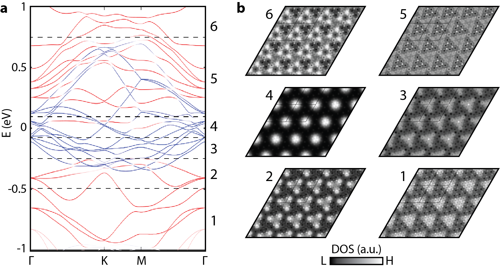
Next from the calculated electronic structure, we simulated STM image of 4Hb-TaS2 1T layer surface. We integrated the charge distribution in the real space following to the specific energy region. The STM pattern from the flat bands, originated from the Mott feature of 1T layer, still sharply localized at the center of SD. On the other hand, the bands near Fermi energy except the flat bands are originated from the other 12 Ta atoms except center of Ta atom. They show slightly delocalized pattern than the flat bands.
S3 QPI of flat bands
We could not detect sharp QPI features in the I/dV maps taken on the 1T termination of 4Hb-TaS2. The wave function distribution over the individual CDW sites appears fairly uniform which may be the cause for the absence of QPI. Still, we could identify faint features in Fourier space. They appeared within the energy window of 0-100 meV within which we find the DFBs. Two examples taken on two distinct 1T surfaces are given in Fig.S5 and S3. In them the Bragg peaks corresponding to the CDW periodicity appear clearly (atomic Bragg peaks are outside the Fourier space shown). Intriguingly, in both QPI maps within the energy range of the DFBs (72 meV cut is shown) we find arc-like features that replicate about the CDW Bragg peak. Such replication means that the wave function of the DFBs follows the periodicity of the CDW rather than the underlying atomic lattice. This suggests that the DFB wavefunction remains rather localized on the CDW sites.
S4 Analysis of ‘dim’ sites in topography
A typical topography of the 1T layer is shown in Fig.S4a (same as Fig.1b). We identify two different types of defects in the CDW superlattice: (i) ‘dim’, as shown in Fig.S4b and (ii) ‘vacancy’, as shown in Fig.S4c. Their reduced height profile readily identifies the ‘dim’ sites compared to the regular (‘bright’) CDW sites. The various CDW sites were identified by appropriately using an intensity threshold and ‘regionprops’ function in MATLAB. The identified ’dim’ sites are overlaid on the topography as shown in Fig.S4d. The ’dim’ sites constitute of the entire CDW sites in this topography. We surmise that the ’vacancy’ in the CDW lattice is due to Ta vacancy and the ’dim’ sites are due to either S vacancy or Se substitution [54].
S5 Kondo resonance
A representative large energy window spectrum of the Kondo resonance is shown in Fig.S8. The spectrum was measured on a ‘dim’ CDW site of the 1T layer (same as Fig. 2a). The conduction and the valence band emerge at high energies meV above and below the Fermi energy (see also Fig.S2a and b). The upper and lower Hubbard bands appear as quasi-particle peaks meV away from the Fermi energy. The sharp zero-bias peak is identified as the Kondo resonance.
S6 Fitting analysis of Kondo resonance
High energy resolution dI/dV profile of a Kondo resonance is shown in Fig.S9a. A smooth polynomial background was subtracted from the dI/dV profile. A fifth-order polynomial was fit to the dark blue circles in Fig.S9a, marked by the dashed purple line. The subtracted profile is shown in Fig.S9b (also in Fig.2b). The Kondo resonance is often fit to a Fano line shape in STM measurements. The Fano line shape is given by , where is the form factor and is the normalized energy with as the resonance position and as the half-width at half-maximum. The dI/dV profile (dark blue circles) in Fig.S9b is fit to , where and are additional fitting parameters. The Fano fit parameters are: q = 22(10), meV, meV. The high value of justifies using a simpler Lorentzian line shape to capture the width of the Kondo resonance. The half-width at half-maximum from both the Fano fit ( meV) and the Lorentzian fit ( meV) are very similar.
S7 Magnetic field response of Kondo resonance
We did not observe any significant change in the Kondo resonance up to the maximum out-of-plane magnetic field of 9T possible to apply in our system (Fig.S10). This lack of magnetic field response could be due to that Zeeman energy at 9T ( meV) is not enough to split the Kondo resonance ( meV) [55].
S8 Spectroscopic maps of Kondo resonance
1D and 2D dI/dV maps similar to Fig.2c are shown in Fig.S12 - S13. Fig.S12a shows the dI/dV measurement across several ’bright’ and a couple of ’dim’ CDW sites. The ’bright’ CDW sites typically show a quasi-particle peak at about 70 meV above the Fermi energy as shown in Fig.S12b (yellow). However, sometimes we also see a spectrum where the quasi-particle peak is closer to the Fermi energy along with a sharp drop in the density of states across the Fermi energy (red). The ’dim’ sites exhibit a robust zero-bias peak (or Kondo resonance) (blue). The Kondo resonance is localized to the ’dim’ CDW site, as also shown in Fig.S11.
2D mapping of the ’dim’ CDW sites reveals the entire spatial distribution of the Kondo resonance (Fig.S13). The topography of the 1T CDW lattice with a single ’dim’ site in the center is shown in Fig.S13a. A 1D dI/dV map across the ’dim’ site, marked by a white dashed line, is shown in Fig.S13b. The dI/dV map measured on Fig.S13a at the Fermi energy is shown in Fig.S13c. The ’dim’ site shown a high density of states corresponding to the Kondo resonance. To better visualize the different types of spectra, we cluster all the spectra measured in this region. The spectra are clustered into three different types denoted by different colors. Fig.S13d shows the spatial region of the different spectra, and Fig.S13e shows the averaged spectra of each type.
S9 Hysteresis
By taking fine steps in tip position about the phase transition point (marked both by an abrupt change of spectrum in Fig.S15a,c as well as by a resulting discontinuous step in tip height in Fig.S15b,d) we find a hysteresis in the tip distance from sample at which the transition takes place between approaching and retracting sweep directions.
S10 Noise
The dI/dV spectra taken about the transition point seem noisier. We quantify this by calculating the standard deviation of the 10 consecutive measurements we take at every energy point (typically we show their mean). In Fig.4a and in Fig.S16a-c we show the mean value of that calculated standard deviation over all energies measured. In rough position sweeps, shown in Fig.S16a,b, we find that the noise increases sharply about the transition point on the ZBCP side of the spectrum (regardless of sweep direction). When we take finer steps about the transition, where we resolve the hysteresis loop, we also find slight asymmetry between approaching and retracting sweeps. On the approaching sweep (orange) the noise rises and drops sharply at the transition point. On the retracting sweep (green) we see a gradual onset of the noise already before it takes place and drops gradually across it. We note that all our measurements are taken with at a very low frequency of about 1 KHz. Therefore, the noise we find has low frequency characteristics. Intriguingly on some of the dim CDW sites we also find a bi-stable noise pattern that switches between two values as shown in the time traces in Fig.S16d,f. They show the tunneling current taken with the feedback loop open, thus reflecting changes in the electronic system of 1T-TaS2 rather than of the tip (we do not detect such behavior away from dim CDW sites). Their histograms, given in Fig.S16e,g, respectively, clearly show bi-stability characteristic of telegraphic noise.
S11 Tip manipulation of the Kondo resonance
The spectroscopy measurements presented in Fig.3 are reversible and reproducible. Similar measurements are presented in Fig.S17 for both tip direction and step heights. The tip-sample distance () is changed by changing the current set-point (). Increasing the decreases the tip-sample distance and vice-versa. Fig.S17a shows the reverse measurement of Fig.3c, i.e., we start with the tip very close to the sample (blue) and gradually withdraw the tip away from the sample (red). We see the reverse phenomenology. When the tip is near the sample, a single quasi-particle peak is observed at meV. This peak splits as the tip-sample distance decreases. Eventually, the spectrum transitions back to the Kondo resonance. Repeating this measurement in the opposite direction with much smaller increments of tip-sample distance leads to the same result as shown in Fig.S17b.
S12 Tip manipulation of flat bands
A higher-energy resolution measurement of Fig.3d is shown in Fig.S18a. We again observe the non-monotonic shift of the peak position (), shown in Fig.S18b and the gradual reduction of the peak width (FWHM), shown in Fig.S18c. Tip-induced band bending usually shifts the band monotonically, and therefore, the non-monotonic shift of the peak remains puzzling. The gradual reduction of the peak width may be interpreted as follows. Although the lower Hubbard band is nearly empty due to charge transfer from the 1T layer to the 1H layer, a part of it may still be occupied. Thus, the quasi-particle peak we observe at meV consists of both the upper and the partially occupied lower Hubbard band whose energy spitting is not resolved due to large peak widths. On bringing the tip closer to the sample, the interlayer coupling could increase, leading to further depletion of the lower Hubbard band. Therefore, fully emptying the lower Hubbard band would make the Hubbard bands degenerate, thus reducing the peak width. This proposal also explains merging the two peaks beyond the quantum phase transition in Fig.3c.
S13 Set-point effect
The raw data of the temperature sweep shown in Fig.3a (also Fig.S19a for comparison) is shown in Fig.S19b. In it we find a sharp change in dI/dV that happens at 3.5 K across all bias. It is an intriguing artifact of the STM measurement (Fig.S19) in which the tip repositions its height in response to a change in the electronic spectrum. The feedback loop fixes the tip height to maintain a desired tunneling current under a fixed bias voltage, here set to 200 meV. That tunneling current is affected mainly by the tunneling matrix element, which is exponentially dependent to distance between the tip and the sample, as well as the integrated DOS from the Fermi level up to the bias voltage above it. If for any reason the sample DOS changes, so will the that integral and the feedback loop will response by readjusting the tip height to maintain constant current. What happens at 3.5 K is that the transition line crosses the parking bias of 200 meV. Once that happens the electronic DOS in the sample undergoes the phase transition from Kondo state at lower temperatures to DFB state above. the non-dispersive step at 3.5K results from repositioning the tip height to maintain constant current for the changing electronic phase. It is a unique manifestation of the well known set-point effect that occurs because the tip is part of the quantum electronic system it probes. However, this is a measurement artifact, and therefore we normalize it out in Fig.3a by fixing a constant dI/dV value at a certain energy (-20 meV) within the DFB high-temperature state (ie 2.5K and above).
S14 Thermodynamics of the first-order transition
To model a first-order phase transition as function of temperature and voltage , we use a Taylor expansion of the free energy of the two phases, , as function of temperature and applied voltage .
| (1) |
where is the entropy of phase , encodes the capacitance of the system in the presence of the tip and with the units of charge denotes a shift of energy linear in the voltage, discussed in more detail below. Note that the sign of the capacitative correction is negative as the system gains energy by moving charge between system and tip. We assume that , thus one obtains a transition from phase to phase upon increasing the temperature.
The thermodynamic first-order transition occurs at a voltage-dependent transition temperature obtained from
| (2) |
Chosing such that , we get
| (3) |
with , , . From a fit to the experiment we find
| (4) |
where we used in the last line microscopic units, the electron charge and the Boltzmann constant , resulting in a small prefactor. This indicates either an almost complete compensation of the change of polarization arising from the transfer of charge beween the layers or a very large entropy of the high-T phase. Note that the phase diagram was measured by reducing the voltage starting from the parking bias mV. Therefore we cannot rule out that a possible hysteresis may affect the value (and even the sign) of but we can exclude a substantially larger value of this quantity.
We can obtain a rough estimate of by using that the electric field at the surface of the sample is of the order of for a flat tip or for a very sharp tip with radius , where nm is the distance of the tip from the surface. If the polarization of the two phases differs by , then the field-induced difference of energies is given by the product of field and polarization. If we assume, for example, that arises from the shift of an electron charge by Å, we obtain . Comparing this with Eq. (4), we conclude that either the difference of polarization is much smaller or the entropy difference of the two phases is relatively large, of the order of .
When discussing the sign of , it is important to realize that the largest contribution to the capacitance is geometric in origin, , and fixed essentially by the shape of the tip and the underlying metalic layers. Only a small extra contribution arises from the local compressibility of the electronic phase just below the tip. The local compressibility can be computed by evaluating to second order in the change of energy arising from a voltage-induced potential (after taking the screening by the metallic substrate into account). As , we conclude that
| (5) |
As the Kondo phase has a much higher local density of states at the Fermi energy, it costs less energy to locally add charges. Thus , which explains why is negative.