Thermal resistance in superconducting flip-chip assemblies
Abstract
Cryogenic microsystems that utilize different 3D integration techniques are being actively developed, e.g., for the needs of quantum technologies. 3D integration can introduce opportunities and challenges to the thermal management of low temperature devices. In this work, we investigate sub-1 K inter-chip thermal resistance of a flip-chip bonded assembly, where two silicon chips are interconnected by compression bonding via indium bumps. The total thermal contact area between the chips is 0.306 mm2 and we find that the temperature dependence of the inter-chip thermal resistance follows the power law of , with K4 µm2/nW. The relation indicates phononic interfacial thermal resistance, which is supported by the vanishing contribution of the electrons to the thermal conduction, due to the superconducting interconnections. Such a thermal resistance value can introduce a thermalization bottleneck in particular at cryogenic temperatures. This can be detrimental for some applications, yet it can also be harnessed. We provide an example of both cases by estimating the parasitic overheating of a cryogenic flip-chip assembly operated under various heat loads as well as simulate the performance of solid-state junction microrefrigerators utilizing the observed thermal isolation.
3D integration techniques enable vertical interconnection of different microsystems in order to enhance the overall system functionality. In general, the techniques provide higher packing density of microcircuits compared to the conventional 2D planar fabrication Garrou, Bower, and Ramm (2008), and importantly, the possibility to interconnect non-monolithically several device layers (chips), which have monolithically incompatible fabrication processes. Recently, 3D integration of the microsystems operated at cryogenic temperatures has gained lots of attention, thanks to the intensive growth of the quantum technology field. For superconducting quantum processors with large qubit counts, 3D integration is a must Rosenberg et al (2017) and different realizations already exist Kosen et al (2022); Conner et al (2021). Large spin-qubit quantum processors and the interfacing Cryo-CMOS peripherals naturally benefit from 3D integration Veldhorst et al. (2017), as well as schemes utilizing 2-qubit coupling with superconducting resonators Holman et al. (2021). Another superconducting component that calls for similar approaches is a vertical solid-state microrefrigerator proposed in Ref. Mykkänen et al. (2020)
3D integration can pose challenges to the thermal management of microsystems Venkatadri, Sammakia, and K. Srihari (2011), and very little is known about the inter-chip thermal resistance in such assemblies at low temperatures. Due to the steep thermal suppression of electron-phonon coupling and interfacial phonon-phonon transport, several cryogenic electronic applications require careful design of the device-to-bath thermal contact stack to prevent overheating even under modest dissipative loads. Large local non-equilibrium populations of phonons can be generated during the operation of microdevices, and these phonons must be efficiently conducted away from the generated hot spots. The heat must be eventually dumped to the thermal bath formed, for example, by the (metallic) sample holder at the cold head of a cryostat. The interfaces and constrictions introduced to such thermalization paths by 3D integration are bound to increase the overall device–to–bath thermal resistance. This can be very beneficial to applications in superconducting solid-state microrefrigerators, provided that the thermal resistance occurs close to the cooled interface.
In this work, we report on sub-1 K thermal resistance characterization of a 3D integrated assembly, where two silicon chips are joined by indium bumps with flip-chip atmospheric compression bonding. We find that the thermal resistance of the device follows power law, with several times larger absolute value than predicted by the diffusive mismatch theory. We simulate phononic power law to show how non-negligible heat loads can pose a thermalization problem in flip-chip devices operating at sub-1 K temperature range. We also provide a simulation of vanadium (V)- and aluminum (Al) based superconducting microrefrigerators using the measured thermal resistance and previously demonstrated junction parameters Kemppinen et al. (2021).
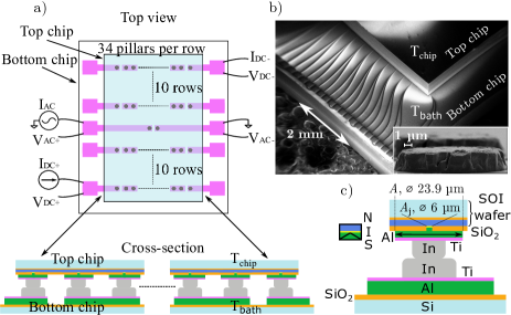
The system analyzed in this letter is a flip-chip device consisting of a bottom chip of 8 x 8 mm2 and a top chip of 4 x 6 mm2 surface footprint. Figure 1a) shows an illustrative schematic of the flip-chip device from the top of the assembly and a cross-section of a single interconnection row. The device comprises a total of 682 interconnection pillars, with two arrays consisting of 340 pillars each, positioned adjacent to the pillar pair depicted at the center of the device. A scanning electron micrograph in Fig. 1b captures the device, alongside a single indium bump before the bonding process. The interconnection of chips is facilitated by indium bumps on both the bottom and top chips, forming a unified interconnection pillar as presented in Fig. 1c. Each of these pillars houses a normal metal–insulator–superconductor (NIS) junction, where the normal metal component consists of a pool of degenerately-doped silicon, common to all of the junctions. In this work, a junction pair in the middle of the device was used as a thermometer to measure the temperature of the top chip as a function of the applied heating power. The heating was applied through two junctions located on the diagonal corners of the device. The experimental connections are highlighted in Fig. 1a) and will be discussed in more detail following the description of the fabrication process.
The bottom chip was fabricated on a 150 mm p-type silicon (Si) wafer using thermal oxide growth (100 nm SiO2), metal sputtering [200 nm Al and 50 nm titanium (Ti)], ultraviolet (UV) lithography and reactive ion etching. In bumps with thicknesses of 3 µm were deposited with an electron-beam evaporator on a patterned 5 µm thick lift-off resist. Prior to the evaporation, the Ti surface was argon-ion beam etched to remove the surface oxide in-situ. After the evaporation, the resist was removed in an acetone bath, completing the bottom chip fabrication. The top chip was fabricated on a 150 mm silicon–on–insulator (SOI) wafer, in which the 40 µm thick device layer has an n-type (phosphorus) doping yielding an electrical resistivity less than 1.5 mcm at room temperature. Additional ion implantation of phosphorus was done with an acceleration voltage of 27 kV and a fluence of 41015 cm-2 to increase the surface dopant concentration. Based on the thermal budget of the following process steps, this yields a total dopant concentration of about 1020 cm-3 for the surface layers. Even though the volumetric electron-phonon coupling in doped semiconductors is lower than that of metals Prunnila et al. (2005), the large volume of the normal metal ( µm3) ensures strong overall coupling. A 100 nm layer of SiO2 was grown on the top chip wafer, followed by the tunnel junction contact etching. The µm2 sized contacts to the Si surface were done by UV lithography combined with plasma- and wet etching. The tunnel barrier was grown thermally by keeping the Si surface under 0.13 mbar of pure oxygen for 10 minutes at 550 ∘C. A 500 nm Al layer and an additional 25 nm Ti layer were sputtered in-situ. The Ti layer functions as an adhesion layer between Al and In, which was deposited, as described above, to complete the top chip fabrication.
We define the thermal interface area per pillar by the tunnel junction area and the surrounding Al collar as shown in Fig. 1c). With 682 pillars in the device, the total thermal interface area is 0.306 mm2. Both wafers were diced to individual chips, with each wafer yielding from a hundred to several hundred devices. The bottom- and the top chips were connected together with a flip-chip bonder using a room temperature compression cycle. The cycle consisted of an alignment-, a chip parallelization- and a 30 second compression step with a force of 6.8 N at 29 ∘C. With the given recipe, we have observed a 50% reduction in the height of the bumps. Under the assumption that the total volume of the bumps remains constant, this transformation results in a twofold expansion of the surface area of the indium. Conversely, the surface area of the indium oxide remains unaltered, leading to an effective In-In contact. The method is discussed more thoroughly in the supplementary material of Ref. Kosen et al (2022). The device was attached to the copper sample holder with a polyvinyl butyral based glue used commonly in experimental low temperature physics. The sample holder was mounted with metallic screws on the mixing chamber flange of a dilution refrigerator to ensure a good thermal contact from the cryostat to the sample holder and the bottom chip. The efficient thermalization allowed us to measure the temperature of the bottom chip with a calibrated ruthenium oxide thermometer positioned on the mixing chamber flange.
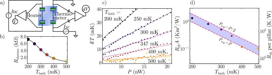
The thermal resistance of the device was determined by heating the top chip with the heater junction pair and measuring the elevated temperature of the top chip with the thermometer junctions at various bath temperatures . Figure 2a) supplements the experimental wiring provided in Fig. 1a). The heater was biased with a floating DC current and the corresponding voltage over the heater was recorded with a junction field-effect transistor amplifier and a digital multimeter. The thermometer was operated with a sinusoidal AC current of 0.5 nA at 18 Hz and the voltage across was recorded with an AC coupled lock-in amplifier. The thermometer was calibrated against the bath temperature by fitting the zero-bias resistance against to a standard model used for NIS junctions Muhonen, Meschke, and Pekola (2012) and assuming that the electron- and the phonon temperatures are equal. The fit yielded a normal state tunneling resistance R 107 , a sub gap leakage parameter 1.410-2 and a critical temperature 1.12 K. Figure 2b) shows the calibration with the data points and the fit line. We note that the self heating of the thermometer was smaller than 2.5 fW, thus negligible compared to the applied heater power values of the order of 10 nW.
Figure 2c) shows the temperature increase of the top chip as a function of the total heating power of the heater junctions for between 200 mK and 500 mK. The relation between and is linear for mK and nW, which corresponds to DC bias voltages above the superconducting energy gap, i.e. for given junction parameters. In this linear regime, the thermal resistance between the bottom and the top chip at given is
| (1) |
where is the power injected to the top chip. For NIS junctions biased at , the heat injected into the normal metal approaches 50% of the total heat generation. Given that a portion of the heat injected into the superconductor might also flow to the top chip due to insufficient quasiparticle evacuation from the vicinity of the junction, in the following we consider the effective heating power to the top chip in to lie in a bracket between the values and .
Scaling the extracted thermal resistances by yields an effective interfacial thermal resistance (eITR), which follows the temperature dependence of Swartz and Pohl (1987)
| (2) |
Figure 2d) shows eITR as a shaded blue area defined by the two dashed red lines, obtained by fitting the constant to the extracted values of at different temperatures. The lower boundary is produced by the assumption of full heat dissipation to the top chip () and the upper boundary by partial dissipation (). The data points correspond to the average of these limits, i.e. 75% of is injected to the normal metal. The lower estimate yields the prefactor of 7.7 K4µm2/nW, which doubles for the upper line fit as 15.4 K4µm2/nW.
Since In is a good thermal conductor at low temperatures Graham2014 and the thicknesses of the rest of the layers along the pillars are smaller than the dominant thermal phonon wavelengths, it is unlikely to have any significant thermal gradients along the interconnecting columns. Hence, we assume the origin of the observed to be of interfacial nature. Adhesion between surfaces is a complex problem involving various types of bondsGerberich_2006. Obtaining high quality metal-insulator interfaces is generally more challenging in comparison with metal-metal contacts due to the different properties of the connecting materials. This points the largest component of the observed eITR to the diffusive Al–SiO2 interfaces at the tunnel junction and the surrounding collar. Due to their largely different oxide thicknesses (below 3 nm at the junction and 100 nm at the collar), these regions may isolate heat at different capacities, yet the two contributions cannot be assessed separately in our measurement. Practically, the effective thermal contact area is dominated by the collar, as its area is relatively large compared with (1:15). The eITR of a metal-substrate interface can be quantitatively described in multiple systems by the acoustic mismatch (AMM) and diffusive mismatch (DMM) models Little (1959); Swartz and Pohl (1987, 1989), which differ minimally at low temperatures. For Al–SiO2, DMM gives a value of K4µm2/nW, whereas our measurements indicate 7.1–14 times larger eITR. Previous works with metal films on oxidized Si substrates have shown up to five times larger eITR compared with DMM calculations Rajauria et al. (2007); Pascal et al. (2013); Wang et al. (2019) and a fourfold increase in eITR has been observed by depositing a thin adhesive Ti layer between a metal and a substrate Wang et al. (2019). Similarly, the multiple interfaces in the inter-chip pillars in our device may contribute non-trivially to additional thermal resistance. DMM predicts a value of 3.5 K4µm2/nW to the full stack, as discussed more in the supplementary material. However, the applicability of the DMM model to the presented system with multiple interfaces is questionable, since modeling the full stack by adding individual interface contributions independently together might not fully capture phonon propagation in a stack with layers of thicknesses comparable to the dominant phonon wavelength.
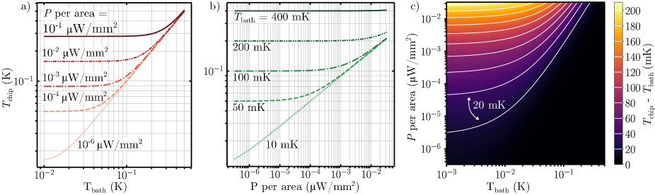
Large eITR can be detrimental for applications requiring good thermal contact, and care must but taken in device design to mitigate potential thermal bottlenecks. However, the large eITR can also be a desired feature in some devices, such as solid-state microrefrigerators. Here, we present simulations supporting both claims. In the following cases, the eITR parameter is set to 15.4 K4µm2/nW. Figure 3 shows the thermal behaviour of a system operating at sub-1 K temperature range with various heat loads per thermal contact area (), which is modelled by solving the phononic heat flow law
| (3) |
where the chip and the thermal bath are decoupled through the thermal resistance characterized by . Equation (3) was solved for varying the power density and the bath temperature . Figure 3a) shows the chip temperature as a function of the bath temperature for few values of power density ( per area). When scaled with the thermal interface area of the device analyzed in this letter, the power values range from around 300 fW to 30 nW. At 10 mK, the usual base temperature of a commercial dilution refrigerator, increasing power density corresponds to an elevated chip temperature of 16 mK at 10-6 µW/mm2 and notably 280 mK at 10-1 µW/mm2. At higher bath temperatures the chip temperature coincide with the bath temperature, i.e. . Figure 3b) shows the temperature of the chip as a function of power density for few values of bath temperature. Again, the chip temperature is elevated significantly at 10 mK with increasing power density. At intermediate temperatures the chip is effectively thermalized to the bath at the lowest power density values and at 400 mK the elevated is negligible even at highest power density values. The overall behaviour is summarized in Fig. 3c), where a colormap shows the absolute overheating of from the bath as a function of the two variables, bath temperature and power density. In conclusion, the simulation exemplifies to what extent the flip-chip stack can act as a thermalization bottleneck at power density values relevant to the devices operating at sub-1 K temperature range. To overcome this, the straightforward approach is to increase the thermal interface area i.e. the diameter and/or amount of the interconnect pillars, when applicable to the device design. However, practical limitations may arise when attempting to optimize interconnect density using the current indium bump technology e.g. due to bonding and fabrication related limits. Although alternative bonding methods, such as Cu-Cu hybrid bondingMoreau et al. (2022), have been developed to enhance interconnect density, there is currently no superconducting interconnect available that offers both low bonding force and temperature, but new methods are actively being developed. We note that normal metal interconnects exhibit a thermal conductivity that encompasses not only phononic but also an electronic contribution, which allows better thermalization for technologies with non-superconducting interconnects.
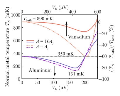
In contrast to the thermalization bottleneck, the large eITR can be harnessed in optimizing superconducting solid-state microrefrigerators. Here we present a simulation of V- and Al based superconducting microrefrigerators by using the eITR prefactor obtained in this work and the junction parameters obtained in our previous work Kemppinen et al. (2021). In the simulation, we assume a strong electron-phonon coupling in the normal metal, such that the electron- and the phonon systems are at an equilibrium temperature i.e. . We also assume that the superconductor is thermalized to the bath temperature, i.e. . The simulation parameters are shown in Tab. 1 and the heat balance is given by
| (4) |
where is the electronic heat flow to the normal metal, is the phononic heat flow to the normal metal from the bath, is the energy, is the voltage bias, is the normalized Dynes density of states of the superconductor and is the Fermi-Dirac distribution of the superconductor (normal metal).
The performance of V- and Al based coolers was estimated by solving from the heat balance equation (Eq. (4)) as a function of for devices with two different ratios between and . The solid lines in Fig. 4 represent a device with an Al collar placed around the junction (), similar to the structure studied in this letter. The dashed lines show approach, where the collar is left out and the heat leakage occurs entirely through the junction (). Here it is assumed, that the eITR is equal at the junction and the collar. The V stage is able to cool down from the bath temperature of 890 mK to 740 mK with the collar structure, and to 350 mK in the approach without collar. The performance of the Al stage is not affected as much due to the dependent heat leak. The Al stage can cool down from 350 mK to 170 mK with the collar, and to 131 mK without it. The relative cooling with V from is 60% at best. We note that the Al stage can, in principle, be thermalized to the V stage to form a two-stage microrefrigerator. More quantitative modeling and discussion of a multi-stage cascaded microrefrigerator can be found in Ref. Kemppinen et al. (2021) including the role of transparency-limited junction leakage.
| Superconductor | ||||
|---|---|---|---|---|
| (K4µm2/nW) | (µm2) | (µ) | ||
| V | 15.4 | 71 | 540 | 610-3 |
| Al | 15.4 | 48 | 182 | 810-3 |
In summary, we have measured the thermal resistance of a superconducting flip-chip assembly at sub-1 K temperatures and compared the result to the DMM theory and previous experiments. Our results exemplify a case in which advanced integration of superconducting assemblies would result in low thermal contact between the chips in 3D integrated assembly. We showed how the thermal resistance can pose a bottleneck for the thermal management of such a system at sub-1 K temperatures due to the demonstrated thermal resistance. We also presented a simulation of the utilization of the measured thermal resistance for the purpose of thermal isolation in V and Al based superconducting solid-state microrefrigerators.
Supplementary Material
The models and parameters used for calculating the diffusive mismatch model predictions for the Al–SiO2 and full material stack are provided as a supplementary material.
Acknowledgements
The authors thank T. Häkkinen, J. Toivonen, L. Grönberg and J. Salonen for technical assistance in the sample fabrication in VTT and OtaNano Micronova cleanroom facilities. We also thank L. Wang for discussions. The research was funded by the European Union’s Horizon 2020 research and innovation programme under grant agreement No. 766853 EFINED, No. 824109 European Microkelvin Platform (EMP), No. 101113086 SoCool and No. 101007322 ECSEL Joint Undertaking (JU), the Academy of Finland through project No. 322580 ETHEC and the QTF Centre of Excellence project No. 336817, Business Finland through Quantum Technology Industrial (QuTI) No. 128291. We also acknowledge Technology Industries of Finland Centennial Foundation for funding.
Author declarations
J. Hätinen contributed to process development, characterization, data analysis and made the first version of the manuscript. E. Mykkänen contributed to characterization, data analysis and writing. K. Viisanen made the theoretical comparison and contributed to the writing. A. Ronzani contributed to the conceptualization, characterization and writing. A. Kemppinen contributed to the conceptualization and writing. L. Lehtisyrjä contributed to the process development and writing. J. S. Lehtinen conceptualized and lead the work, contributed to the process development, characterization and writing. M. Prunnila conceptualized and supervised the work, and contributed to the writing.
The authors have no conflicts to disclose.
Data availability
The data that support the findings of this study are available from the corresponding author upon reasonable request.
References
References
- Garrou, Bower, and Ramm (2008) P. Garrou, C. Bower, and P. Ramm, “Handbook of 3D integration,” Wiley-VCH (2008).
- Rosenberg et al (2017) D. Rosenberg et al, “3d integrated superconducting qubits,” npj Quantum Inf 3, 42 (2017).
- Kosen et al (2022) S. Kosen et al, “Building blocks of a flip-chip integrated superconducting quantum processor,” Quantum Sci. Technol. 7, 035018 (2022).
- Conner et al (2021) C. R. Conner et al, “Superconducting qubits in a flip-chip architecture,” Appl. Phys. Lett. 118, 232602 (2021).
- Veldhorst et al. (2017) M. Veldhorst, H. G. J. Eenink, C. H. Yang, and A. S. Dzurak, “Silicon cmos architecture for a spin-based quantum computer,” Nat Commun 8, 1766 (2017).
- Holman et al. (2021) N. Holman, D. Rosenberg, D. Yost, J. L. Yoder, R. Das, W. D. Oliver, R. McDermott, and M. A. Eriksson, “3d integration and measurement of a semiconductor double quantum dot with a high-impedance tin resonator,” npj Quantum Inf 7, 137 (2021).
- Mykkänen et al. (2020) E. Mykkänen, J. S. Lehtinen, L. Grönberg, A. Shchepetov, A. V. Timofeev, D. Gunnarsson, A. Kemppinen, A. J. Manninen, and M. Prunnila, “Thermionic junction devices utilizing phonon blocking,” Sci. Adv. 6, eaax9191 (2020).
- Venkatadri, Sammakia, and K. Srihari (2011) V. Venkatadri, B. Sammakia, and D. S. K. Srihari, “A review of recent advances in thermal management in three dimensional chip stacks in electronic systems,” J. Electron. Packag. 133, 041011 (2011).
- Kemppinen et al. (2021) A. Kemppinen, A. Ronzani, E. Mykkänen, J. Hätinen, J. S. Lehtinen, and M. Prunnila, “Cascaded superconducting junction refrigerators: Optimization and performance limits,” Appl. Phys. Lett. 119, 052603 (2021).
- Prunnila et al. (2005) M. Prunnila, P. Kivinen, A. Savin, P. Törmä, and J. Ahopelto, “Intervalley-scattering-induced electron-phonon energy relaxation in many-valley semiconductors at low temperatures,” Phys. Rev. Lett. 95, 206602 (2005).
- Muhonen, Meschke, and Pekola (2012) J. T. Muhonen, M. Meschke, and J. P. Pekola, “Micrometre-scale refrigerators,” Rep. Prog. Phys 75, 046501 (2012).
- Swartz and Pohl (1987) E. T. Swartz and R. O. Pohl, “Thermal resistance at interfaces,” Appl. Phys. Lett. 51, 2200 (1987).
- Little (1959) W. A. Little, “The transport of heat between dissimilar solids at low temperatures,” Can. J. Phys 37, 334 (1959).
- Swartz and Pohl (1989) E. T. Swartz and R. O. Pohl, “Thermal boundary resistance,” Rev. Mod. Phys. 61, 605–668 (1989).
- Rajauria et al. (2007) S. Rajauria, P. S. Luo, T. Fournier, F. W. J. Hekking, H. Courtois, and B. Pannetier, “Electron and phonon cooling in a superconductor–normal-metal–superconductor tunnel junction,” Phys. Rev. Lett. 99, 047004 (2007).
- Pascal et al. (2013) L. Pascal, A. Fay, C. Winkelmann, and H. Courtois, “Existence of an independent phonon bath in a quantum device,” Phys. Rev. B 88, 100502 (2013).
- Wang et al. (2019) L. B. Wang, O.-P. Saira, D. S. Golubev, and J. P. Pekola, “Crossover between electron-phonon and boundary-resistance limits to thermal relaxation in copper films,” Phys. Rev. Applied 12, 024051 (2019).
- Moreau et al. (2022) S. Moreau, J. Jourdon, S. Lhostis, D. Bouchu, B. Ayoub, L. Arnaud, and H. Frémont, “Review—-hybrid bonding-based interconnects: A status on the last robustness and reliability achievements,” ECS J. Solid State Sci. Technol. 11, 024001 (2022).