Ising Superconductivity and Nematicity in Bernal Bilayer Graphene with Strong Spin Orbit Coupling
Abstract
Superconductivity is a ubiquitous feature of graphite allotropes, having been observed in Bernal bilayers, rhombohedral trilayers, and a wide variety of angle-misaligned multilayers. Despite significant differences in the electronic structure across these systems, supporting the graphite layer on a WSe2 substrate has been consistently observed to expand the range of superconductivity in carrier density and temperature. Here, we report the observation of two distinct superconducting states (denoted SC1 and SC2) in Bernal bilayer graphene with strong proximity-induced Ising spin-orbit coupling. Quantum oscillations show that while the normal state of SC1 is consistent with the single-particle band structure, SC2 emerges from a nematic normal state with broken rotational symmetry. Both superconductors are robust to in-plane magnetic fields, violating the paramagnetic limit as expected for spin-valley locked Ising superconductors. Our results show that the enhancement of superconductivity in WSe2 supported graphite allotropes can be directly linked to Ising spin orbit coupling, which favors valley-balanced ground states with time-reversal symmetric Fermi surfaces friendly to superconducting pairing.
Spin-orbit coupling (SOC) preserves the time reversal symmetry of electron bands in solids. As a result, SOC does not have a systematic effect on the superconducting transition temperature: Cooper pairs may still condensed from the degenerate Kramers’ doublets by the same attractive interactions that lead to superconductivity in its absence[1, 2]. Within a weak-coupling Bardeen-Cooper-Schrieffer picture, SOC may either raise or lower the density of states with opposite consequences for . However, SOC does typically make superconductors more resilient to applied magnetic fields by fixing the spin texture of the electron bands. One example is Ising superconductivity[3, 4, 5], where locking between the spins and an internal ‘valley’ degree of freedom renders the band wave functions—and thus the superconducting condensate—nearly immune to applied in-plane magnetic fields.
Graphene[6, 7, 8, 9, 10, 11, 12, 13, 14] provides a unique venue to investigate the interplay of superconductivity and spin-orbit coupling. Due to the small atomic number of carbon, the atomic SOC in graphene is negligible[15]. However, SOC may be induced by supporting the graphene layers on a transition metal dichalcogenide substrate such as WSe2[16, 17, 18, 19, 20, 21, 22, 23]. The existing literature appears to show a systematic enhancement of superconducting transition temperatures for graphene systems with induced spin-orbit coupling. For example, twisted bilayer and trilayer graphene on WSe2 substrates was observed to superconduct for a wider range of angles[24, 25], while in twisted double bilayer graphene [26, 27, 28, 29, 30] superconductivity has been observed only on WSe2 substrates[31]. However, the lack of reproducibility in graphene moiré systems[32] makes controlled experiments difficult.
Recently, it was shown that supporting Bernal bilayer graphene (BBG) on a WSe2 substrate increases the maximal superconducting by an order of magnitude and dramatically expands the domain of carrier density and applied electric displacement field over which superconductivity is observed[33]. BBG is an ideal candidate to quantitatively study the effect of proximity induced SOC on superconductivity. First, the magnetic and superconducting phase diagram of hexagonal boron nitride supported BBG is highly reproducible[14, 34], allowing for reliable experimental controls for the effects of SOC. Second, the magnitude of the proximity-induced Ising SOC can be precisely determined in situ using Landau level coincidences[35]. Finally, the simplicity of the BBG band structure allows for detailed comparisons between experiment and theoretical calculations.
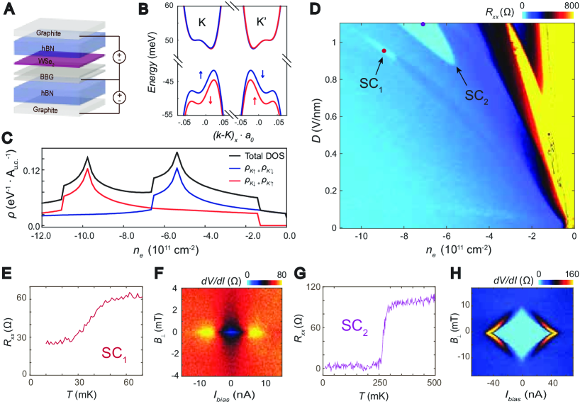
Here, we study a WSe2-supported Bernal bilayer graphene device (Fig. 1A) with a measured proximity-induced Ising spin orbit coupling meV (see Fig. S1). We focus on hole filling and applied electric displacement fields . IN this regime, electronic states near the Fermi energy are polarized on the layer adjacent to the WSe2[35, 33]. Fig. 1B shows the low energy band structure calculated within a tight binding model[36] for an inter-layer potential of 100 meV, which corresponds to a displacement field 1 V/nm [37]. In the low density regime of 10, the measured Ising SOC is comparable to the Fermi energy, breaking the the native four-fold degeneracy of the spins and valleys and leaving a two-fold degeneracy between pairs of spin-valley locked bands. As shown in Fig. 1C, for meV the single-particle density of states is characterized by two well-separated van-Hove singularities, corresponding to the saddle points in each degenerate pair of spin/valley locked bands. Absent Ising SOC, the density of states of regular BBG displays only one van-Hove singularity[14].
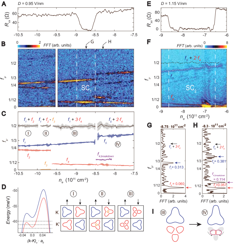
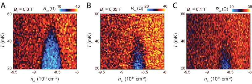
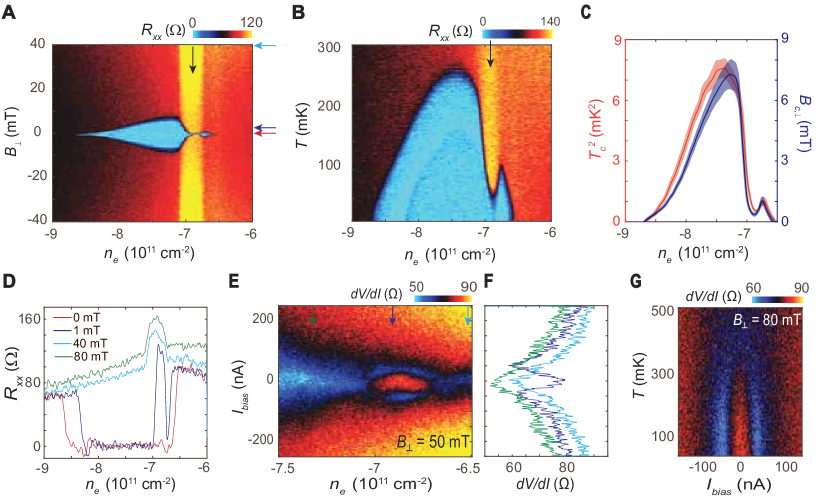
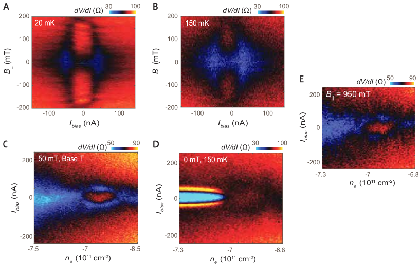
Fig. 1D shows electrical transport measurements for low hole densities and as a function of displacement field. For large displacement fields, we find two distinct superconducting states which we refer to as SC1 and SC2. SC1 has a transition temperature 40 mK, just above the base temperature of our dilution refrigerator. As a result the resistance does not reach zero, showing a saturation at the lowest temperatures (Fig. 1E) that we attribute to disequilibration of the electron system with the phonon bath (see also Fig. S13). However, nonlinear transport measurements in an applied perpendicular magnetic field (Fig. 1F) show both strong non-linearities at sub-10 nA currents and exceptional magnetic field sensitivity characteristic of low- superconductors in crystalline graphene systems[13, 14]. As shown in Fig. 1G, SC2 has a much higher maximum transition temperature. By fitting the non-linear voltage to a Berezinskii–Kosterlitz–Thouless model [38, 39], we find 255 mK (Fig. S2). The dependence shows a critical field of (Fig.‘1H), in line with previous reports of superconductivity in this regime[33].
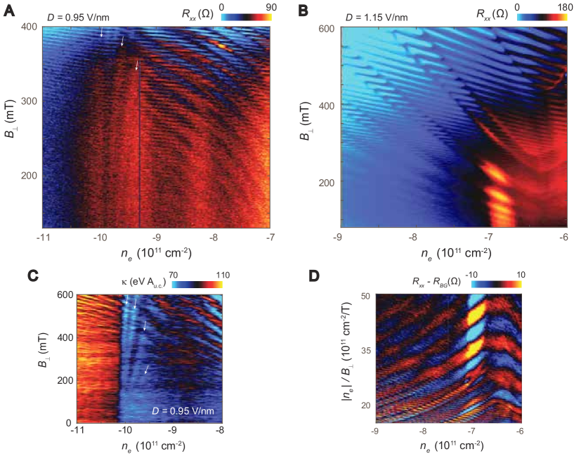
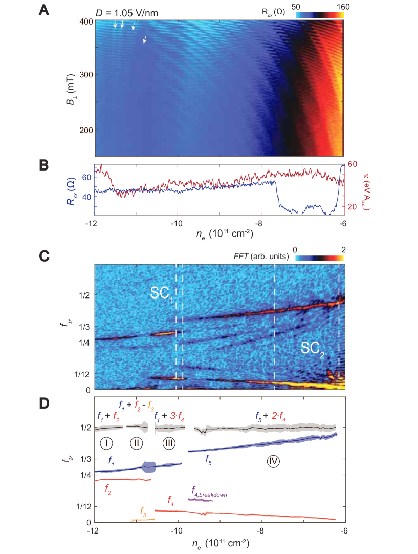
To understand the normal phases from which these superconducting states condensed, we perform high-resolution Shubnikov-de-Haas oscillation measurements, from which we resolve fine details of the Fermi surfaces. Fig. 2A, B show a comparison between zero magnetic field transport and the quantum oscillation frequencies at = 0.95 V/nm, across the domain of SC1. Here, denotes the quantum oscillation frequency normalized to the total carrier density. thus represents the fraction of the total Luttinger volume encircled by a given phase coherent orbit in momentum space. In these units, Luttinger’s theorem may be expressed as
| (1) |
where the index runs over all peaks corresponding to single orbits of a Fermi surface and is an integer degeneracy and carrier sign for the Fermi surfaces producing the oscillation at frequency .
Fig. 2C distills the data of Fig. 2B by plotting only the center frequencies and standard deviations extracted from Gaussian fits of the observed peaks. Across the density range corresponding to regions I, II, and III, the oscillation frequencies can be understood from the SOC-modified single-particle band structure of Fig. 1B-C. For example, region I shows two peaks with slightly different frequencies, denoted and , where = 1/2 within experimental error. Using Eq.1, we see that Luttinger’s theorem may be satisfied by assigning a two fold degeneracy to both Fermi surfaces, . As shown in Fig. 2D, this is consistent with SOC-modified band structure where the favored- and disfavored spin-valley locked bands have slightly mismatched Fermi surface areas even at comparatively high densities. We denote this state Ising2,2. In region II, we observe the emergence of an additional peak, . Due to its low frequency, is barely visible in Fig. 2B but can clearly be identified in the raw resistance and capacitance measurements (see Fig. S3). This is again consistent with band structure, and marks the formation of an annular Fermi sea with both hole-like and electron-like Fermi surfaces. The sum rule implied by the band structure model, = 1/2 is again consistent with experimental data, and we denote this state Ising2,2,-2. In region III, both and vanish and are replaced by a peak at intermediate frequency . The Luttinger sum rule is satisfied for and , as expected after the minority-occupation bands cross the saddle point and each annular Fermi sea breaks into three pockets. We label this state Ising2,6, and conclude that SC1 emerges from a normal state with no additional broken symmetries as compared to the single particle picture.
At the low- boundary of SC1, abruptly disappears and is replaced by a peak () at higher frequency and a peak at frequency , while continues its linear trend. The fermiology of region IV is consistent across a large domain of and , including the entire domain of SC2, as shown in Figs. 2E, F for the highest accessible displacement field and in Fig. S5 at = 1.05 V/nm for a larger density range. This is unexpected within the single particle picture, which cannot account for the emergence of a larger peak as is lowered.
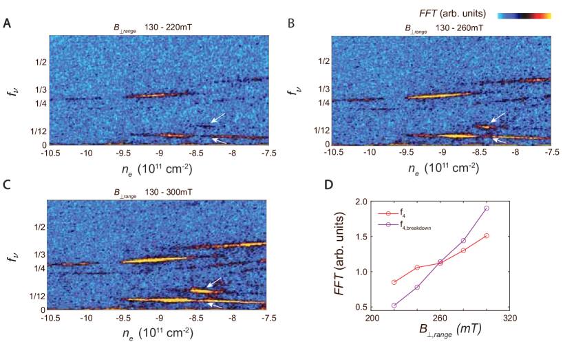
As shown in Fig. S4, the peak at can be attributed to ‘magnetic breakdown’[40] between the Fermi surfaces represented by , and we denote it ; as a result, it should not be counted towards the sum rule of Eq.(1). Remarkably, among simple possibilities, Luttinger’s theorem is satisfied only for and (Fig. 2G, H). This assignment implies that for a single spin-valley flavor in a minority band, the Fermi surface degeneracy is 2—a fact plainly incompatible with preserving the C3 point group symmetry of bilayer graphene. We conclude that the parent state of SC2, and adjoining state to SC1, is nematic and we denote it N2,4. Notably, most prior experiments probing possible nematicity in graphene devices[41, 42, 25, 43, 44] have focused on resistance anisotropy or quantitative interpretation of gap sizes[45]. They rely on assumptions about rotational symmetries of the physical devices or theoretical models that are, at best, approximate. The degeneracy of quantum oscillations, as a probe of closed electron orbits in the sample bulk, provides an unambiguous detection scheme for nematic order that is immune to many of these possible sources of systematic error.
Incidentally, attributing region IV to a nematic phase provides a natural explanation for the observation of the magnetic breakdown peak . Breaking symmetry relaxes the requirement that the small Fermi pockets be arranged symmetrically around the K and K’ points. In this picture, the two small pockets remaining in the phase may move in momentum space to balance the competing effects of the kinetic and exchange contributions to the total energy; Fig. 2I illustrates a schematic representation of the fermiology in the phase near the III-IV transition where the pockets are very close, enabling breakdown. As the density is tuned deeper into region IV, the breakdown signal at fades, implying that the pockets eventually decouple, growing farther apart in momentum space as they shrink in relative volume.
Theoretically, a variety of nematic phases have been proposed throughout the phase diagrams of Bernal and rhombohedral graphene[46, 47, 45, 48, 49, 50, 33, 51]. These include a variety of phases with differing isospin orders, including phases that conserve the occupation of the two valleys separately and those that develop inter-valley coherence[48, 52, 49, 33, 53]. While quantum oscillations alone are not able to resolve these states directly, the phenomenology of SC2, which develops in the phase, allows us to rule out at least some possibilities.
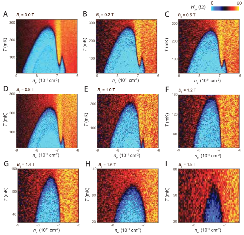
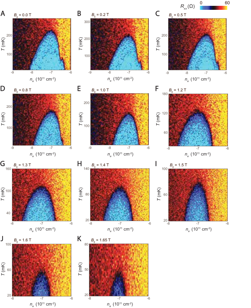
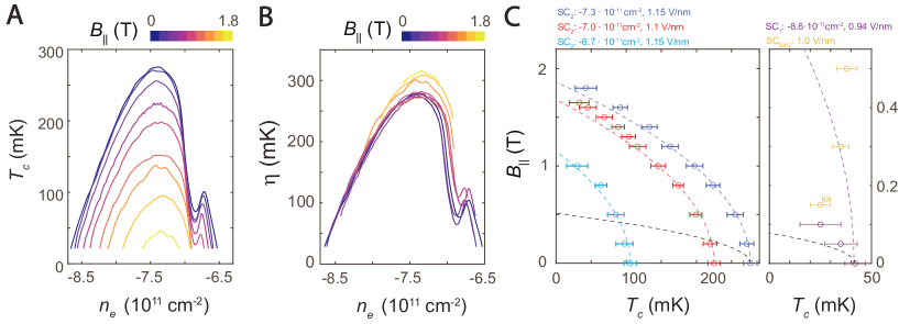
Fig. 3A shows as a function of the in-plane magnetic field, , at = 1.15 V/nm for SC2 (see also Fig. S8 for data from SC1). Within BCS theory, the paramagnetic limit for a spin-singlet superconductor is given by , yielding 500 mT for the maximum 300 mK. SC2 violates the paramagnetic limit by a significant factor across its entire range, with superconductivity still present at fields exceeding 1.8 T. Of course, in the presence of Ising SOC, it is natural to consider the reduced susceptibility of superconductivity to in-plane magnetic fields due to the locking of spins and valleys[1, 2, 54]. In such ‘Ising superconductors,’ pair-breaking by is strongly suppressed by the effective Ising SOC field defined by = , giving[4]
| (2) |
Where is the critical temperature for .
Eq. (2) implies that the ratio should be a constant at all values of following the density dependence of the superconducting dome at zero magnetic field. In Fig. 3B, we show derived from the experimental data in panel A. Indeed, the curves collapse to a high degree of precision, strongly supporting the idea that SC2 is an Ising superconductor throughout its observed range. This remains true across the suppression in observed near = -6.9 1011 cm-2. As shown in Figs. S9, S10, S11, this minimum occurs due to the incursion of a competing ordered state similar to that observed at zero magnetic field in hBN supported bilayer graphene. Notably, however, in the current experiment this phase is favored by magnetic field–opposite the spin-orbit free case[14]. The presence of this competing order impacts quantitatively but does not appear to affect the pair breaking magnetic field (for additional notes on the data on the competing state see SI). Further direct comparison of the data to Eq. (2) are shown in Fig. 3C within SC2. We stress that is measured independently, so that the observed scaling collapse contains no adjustable parameters. This quantitative agreement implies that pairing occurs between Fermi surfaces of definite spin. Any intervalley coherence, therefore, must preserve spin as a good quantum number, in addition to preserving the time reversal symmetry required for efficient pairing in a non-centrosymmetric system.
In other examples of Ising superconductivity such as ion-gated MoS2[3, 5], NbSe2[4, 55, 56], intercalated NbSe2[57], TaS2[56], WS2[58], PdTe2[59] or thin-film Pb[60], cannot typically be measured in situ. The same is true for other superconducting graphene systems supported on WSe2, including [24, 25, 31], raising the natural question of whether induced Ising SOC is sufficient to explain the enhancement of superconductivity in these systems. The induced for graphene on WSe2 is theoretically expected[61, 62, 63] and experimentally obsered to fall between 0.7 - 2.0 meV[35, 33]. The enhancement of due to Ising SOC can thus be estimated across systems. In this analysis, the critical temperatures and fields reported in twisted trilayer graphene[25] as well as twisted double bilayer graphene (tDBG)[31] are in good agreement with Ising superconductivity. In BBG on WSe2 with a smaller 0.7 meV, the paramagnetic limit violation ratio is density dependent. However, at the lowest densities, this ratio reaches precisely the value expected from(Eq. (2)) and never exceeds the limit expected by Ising SC throughout the experimental range. Similarly, as shown in Fig. 3C, SC1 in the present study also violates the paramagnetic limit but does not saturate Eq. (2).
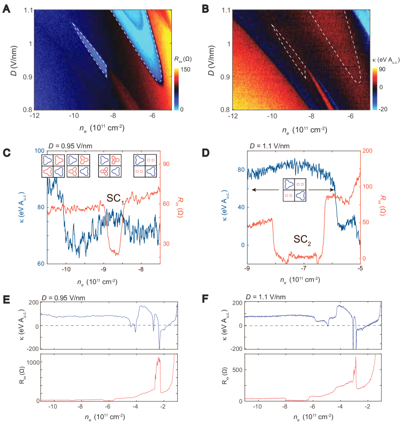
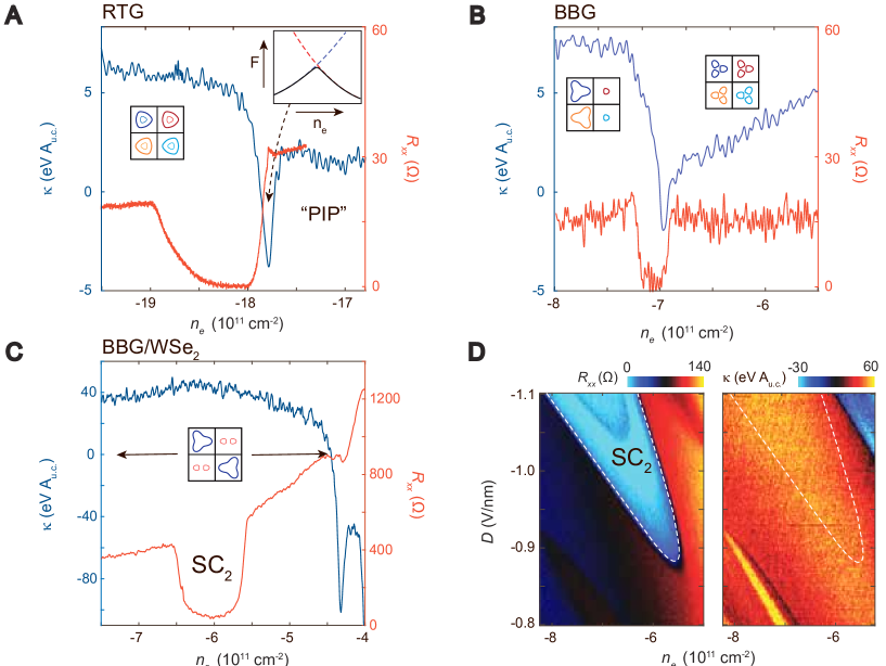
We conclude by contrasting superconductivity in BBG/WSe2 with crystalline graphene superconductors without proximity induced SOC. In these systems, superconductivity has been observed only near isospin phase transitions[13, 14]. However, the nature of these transitions has not been experimentally determined. To characterize the phase transitions and their connection to superconductivity, we measure both resistance and the inverse electronic compressibility . We take pains to measure these simultaneously, ensuring that compressibility measurements are taken under identical conditions, and do no heat the electron systems (see Fig. S14 and Methods). Fig. 4A shows the comparison of and for rhombohedral trilayer (RTG). The isospsin transition between the isospin unpolarized state and the partially isospin polarized state (PIP) is first order, as indicated by the negative compressibility peak (see Fig. 4A inset) observed at the phase boundary. In this regime, superconductivity is observed on the isospin-disordered side of the phase boundary. Fig. 4B shows the same comparison for BBG, taken in the high-D, high regime where triplet superconductivity is observed. Again, superconductivity occurs immediately adjacent to a first order phase transition, in this case on the isospin-ordered side.
In BBG/WSe2, the evolution of the isospin polarization near SC1 bears a superficial resemblance to these systems, with superconductivity developing adjacent to a phase boundary (Fig. S12). However, the phenomenology of SC2 contrasts markedly: as illustrated in Fig. 4C, superconductivity emerges deep within the nematic N2,4 phase, far from any isospin phase transitions. This is corroborated by Fig. 4D, which compares transport and compressibility across a wide range of and ; the domain of superconductivity approaches a first order isospin transition only at the largest displacement fields, but is otherwise uncorrelated. The lack of direct correlation between superconductivity and phase boundaries is also evident in the quantum oscillation data of Fig. 2F, where superconductivity develops, peaks, and subsides over a range for which fermiology evolves monotonically.
These observations suggest that the observed correlation between superconductivity and phase transitions in crystalline graphene layers is likely coincidental. Rather, superconductivity evolves within a given phase but may be destroyed if a competing phase with different symmetry becomes energetically favorable. Within this picture, the enhancement of superconductivity in WSe2-supported graphene devices arises from the broken ‘spinless’ time reversal symmetry relating wave-functions in opposite valleys with the same spin. Breaking this symmetry at the single-particle level preferentially stabilizes a subset of orders featuring two-particle states near the Fermi level compatible with Cooper pairing[1, 2]. It then becomes possible to trace the evolution of superconductivity within a single phase to its maximum strength. SOC may also suppress fluctuations of electronic orders which may suppress superconductivity[51, 53, 64]. In the case of the valley-symmetric nematic order depicted in Fig. 2I, - and -tuned details of the electron wavefunctions near the Fermi surface must then account for non-monotonic dependence of the transition temperature across extent of the phase.
By breaking a symmetry not required for superconductivity (spinless time reversal), SOC stabilizes electronic orders with higher superconducting , including nematic states. In the future, this procedure may be generalized, for example by applying uniaxial strain. Coupling of the strain to a nematic order parameter would then increase the range of stability of the phase, possibly further enhancing superconductivity. Of course, the strong SOC might also be used to generate new superconducting phases in its own right. For example, as is evident in Fig. 3B-C, for the highest values of the superconducting critical field exceeds the Ising limit, a phenomenology expected for finite-momentum Cooper pairing [65, 66]. Experiments in confined geometries such as quantum point contacts might directly access the expected spatial modulation of the superconducting order parameter in these exotic states.
Acknowledgements. The authors would like to acknowledge discussions with E. Berg, Maksym Serbyn, Areg Ghazaryan, A. H. MacDonald, Zhiyu Dong, and Patrick A. Lee. The work was supported by the Office of Naval Research under award N00014-20-1-2609, and the Gordon and Betty Moore Foundation under award GBMF9471. Work at Caltech has been supported by the NSF-CAREER award (DMR-1753306). K.W. and T.T. acknowledge support from the Elemental Strategy Initiative conducted by the MEXT, Japan (Grant Number JPMXP0112101001) and JSPSKAKENHI (Grant Numbers 19H05790, 20H00354 and 21H05233).
References
- Sigrist et al. [2009] M. Sigrist, A. Avella, and F. Mancini, in AIP Conference Proceedings, Vol. 55 (AIP, 2009) pp. 55–96.
- Bauer and Sigrist [2012] E. Bauer and M. Sigrist, eds., Non-Centrosymmetric Superconductors, Lecture Notes in Physics, Vol. 847 (Springer Berlin Heidelberg, Berlin, Heidelberg, 2012).
- Lu et al. [2015] J. M. Lu, O. Zheliuk, I. Leermakers, N. F. Yuan, U. Zeitler, K. T. Law, and J. T. Ye, Science 350, 1353 (2015).
- Xi et al. [2016] X. Xi, Z. Wang, W. Zhao, J. H. Park, K. T. Law, H. Berger, L. Forró, J. Shan, and K. F. Mak, Nature Physics 12, 139 (2016).
- Saito et al. [2016] Y. Saito, Y. Nakamura, M. S. Bahramy, Y. Kohama, J. Ye, Y. Kasahara, Y. Nakagawa, M. Onga, M. Tokunaga, T. Nojima, Y. Yanase, and Y. Iwasa, Nature Physics 12, 144 (2016).
- Cao et al. [2018] Y. Cao, V. Fatemi, S. Fang, K. Watanabe, T. Taniguchi, E. Kaxiras, and P. Jarillo-Herrero, Nature 556, 43 (2018).
- Yankowitz et al. [2019] M. Yankowitz, S. Chen, H. Polshyn, Y. Zhang, K. Watanabe, T. Taniguchi, D. Graf, A. F. Young, and C. R. Dean, Science 363, 1059 (2019).
- Hao et al. [2021] Z. Hao, A. M. Zimmerman, P. Ledwith, E. Khalaf, D. H. Najafabadi, K. Watanabe, T. Taniguchi, A. Vishwanath, and P. Kim, Science 371, 1133 (2021).
- Park et al. [2021] J. M. Park, Y. Cao, K. Watanabe, T. Taniguchi, and P. Jarillo-Herrero, Nature 590, 249 (2021).
- Cao et al. [2021a] Y. Cao, J. M. Park, K. Watanabe, T. Taniguchi, and P. Jarillo-Herrero, Nature 595, 526 (2021a).
- Zhang et al. [2022a] Y. Zhang, R. Polski, C. Lewandowski, A. Thomson, Y. Peng, Y. Choi, H. Kim, K. Watanabe, T. Taniguchi, J. Alicea, F. von Oppen, G. Refael, and S. Nadj-Perge, Science 377, 1538 (2022a).
- Park et al. [2022] J. M. Park, Y. Cao, L. Q. Xia, S. Sun, K. Watanabe, T. Taniguchi, and P. Jarillo-Herrero, Nature Materials 21, 877 (2022).
- Zhou et al. [2021a] H. Zhou, T. Xie, T. Taniguchi, K. Watanabe, and A. F. Young, Nature 598, 434 (2021a).
- Zhou et al. [2022] H. Zhou, L. Holleis, Y. Saito, L. Cohen, W. Huynh, C. L. Patterson, F. Yang, T. Taniguchi, K. Watanabe, and A. F. Young, Science 375, 774 (2022).
- Sichau et al. [2019] J. Sichau, M. Prada, T. Anlauf, T. J. Lyon, B. Bosnjak, L. Tiemann, and R. H. Blick, Physical Review Letters 122, 46403 (2019).
- Avsar et al. [2014] A. Avsar, J. Y. Tan, T. Taychatanapat, J. Balakrishnan, G. K. Koon, Y. Yeo, J. Lahiri, A. Carvalho, A. S. Rodin, E. C. O’Farrell, G. Eda, A. H. Castro Neto, and B. Özyilmaz, Nature Communications 5, 1 (2014).
- Wang et al. [2015] Z. Wang, D. K. Ki, H. Chen, H. Berger, A. H. MacDonald, and A. F. Morpurgo, Nature Communications 6, 1 (2015).
- Wang et al. [2016] Z. Wang, D. K. Ki, J. Y. Khoo, D. Mauro, H. Berger, L. S. Levitov, and A. F. Morpurgo, Physical Review X 6, 1 (2016).
- Yang et al. [2017] B. Yang, M. Lohmann, D. Barroso, I. Liao, Z. Lin, Y. Liu, L. Bartels, K. Watanabe, T. Taniguchi, and J. Shi, Physical Review B 96, 1 (2017).
- Völkl et al. [2017] T. Völkl, T. Rockinger, M. Drienovsky, K. Watanabe, T. Taniguchi, D. Weiss, and J. Eroms, Physical Review B 96, 1 (2017).
- Zihlmann et al. [2018] S. Zihlmann, A. W. Cummings, J. H. Garcia, M. Kedves, K. Watanabe, T. Taniguchi, C. Schönenberger, and P. Makk, Physical Review B 97, 1 (2018).
- Wakamura et al. [2018] T. Wakamura, F. Reale, P. Palczynski, S. Guéron, C. Mattevi, and H. Bouchiat, Physical Review Letters 120, 1 (2018).
- Wang et al. [2019] D. Wang, S. Che, G. Cao, R. Lyu, K. Watanabe, T. Taniguchi, C. N. Lau, and M. Bockrath, Nano Letters 19, 7028 (2019).
- Arora et al. [2020] H. S. Arora, R. Polski, Y. Zhang, A. Thomson, Y. Choi, H. Kim, Z. Lin, I. Z. Wilson, X. Xu, J.-H. Chu, K. Watanabe, T. Taniguchi, J. Alicea, S. Nadj-Perge, and Y. Zhang, Nature 583, 379 (2020).
- Lin et al. [2022] J. X. Lin, P. Siriviboon, H. D. Scammell, S. Liu, D. Rhodes, K. Watanabe, T. Taniguchi, J. Hone, M. S. Scheurer, and J. I. Li, Nature Physics 18, 1221 (2022).
- Burg et al. [2019] G. W. Burg, J. Zhu, T. Taniguchi, K. Watanabe, A. H. Macdonald, and E. Tutuc, Physical Review Letters 123, 197702 (2019).
- Shen et al. [2020] C. Shen, Y. Chu, Q. S. Wu, N. Li, S. Wang, Y. Zhao, J. Tang, J. Liu, J. Tian, K. Watanabe, T. Taniguchi, R. Yang, Z. Y. Meng, D. Shi, O. V. Yazyev, and G. Zhang, Nature Physics 16, 520 (2020).
- Najafabadi et al. [2020] D. H. Najafabadi, K. Watanabe, T. Taniguchi, A. Vishwanath, and P. Kim, Nature 583 (2020), 10.1038/s41586-020-2458-7.
- Cao et al. [2020] Y. Cao, T. Taniguchi, and P. Jarillo-herrero, Nature 583 (2020), 10.1038/s41586-020-2260-6.
- He et al. [2021] M. He, Y. Li, J. Cai, Y. Liu, K. Watanabe, T. Taniguchi, X. Xu, and M. Yankowitz, Nature Physics 17 (2021), 10.1038/s41567-020-1030-6.
- Su et al. [2022] R. Su, M. Kuiri, K. Watanabe, T. Taniguchi, and J. Folk, arXiv (2022), arXiv:2211.16449 .
- Lau et al. [2022] C. N. Lau, M. W. Bockrath, K. F. Mak, and F. Zhang, Nature 602, 41 (2022).
- Zhang et al. [2023] Y. Zhang, R. Polski, A. Thomson, E. Lantagne-Hurtubise, C. Lewandowski, H. Zhou, K. Watanabe, T. Taniguchi, J. Alicea, and S. Nadj-Perge, Nature 613, 268 (2023).
- de la Barrera et al. [2022] S. C. de la Barrera, S. Aronson, Z. Zheng, K. Watanabe, T. Taniguchi, Q. Ma, P. Jarillo-Herrero, and R. Ashoori, Nature Physics 18, 771 (2022).
- Island et al. [2019] J. O. Island, X. Cui, C. Lewandowski, J. Y. Khoo, E. M. Spanton, H. Zhou, D. Rhodes, J. C. Hone, T. Taniguchi, K. Watanabe, L. S. Levitov, M. P. Zaletel, and A. F. Young, Nature 571, 85 (2019).
- Jung and MacDonald [2014] J. Jung and A. H. MacDonald, Physical Review B 89, 035405 (2014).
- Zhang et al. [2009] Y. Zhang, T. T. Tang, C. Girit, Z. Hao, M. C. Martin, A. Zettl, M. F. Crommie, Y. R. Shen, and F. Wang, Nature 459, 820 (2009).
- Berezinskii [1971] V. L. Berezinskii, Sov. Phys. JETP 32, 493 (1971).
- Kosterlitz and Thouless [1973] J. M. Kosterlitz and D. J. Thouless, J. Phys. C : Solid State Phys 6 (1973).
- Biberacher [2005] W. Biberacher, Encyclopedia of Condensed Matter Physics , 360 (2005).
- Cao et al. [2021b] Y. Cao, D. Rodan-Legrain, J. M. Park, N. F. Yuan, K. Watanabe, T. Taniguchi, R. M. Fernandes, L. Fu, and P. Jarillo-Herrero, Science 372, 264 (2021b).
- Lin et al. [2023] J.-X. Lin, Y. Wang, N. J. Zhang, K. Watanabe, T. Taniguchi, L. Fu, and J. I. A. Li, arXiv , 1 (2023), arXiv:2302.04261 .
- Zhang et al. [2022b] N. J. Zhang, Y. Wang, K. Watanabe, T. Taniguchi, O. Vafek, and J. I. A. Li, arXiv , 1 (2022b), arXiv:2211.01352 .
- Zhang et al. [2022c] N. J. Zhang, J.-X. Lin, Y. Wang, K. Watanabe, T. Taniguchi, L. Fu, and J. I. A. Li, arXiv , 1 (2022c), arXiv:2209.12964 .
- Mayorov et al. [2011] A. S. Mayorov, D. C. Elias, M. Mucha-Kruczynski, R. V. Gorbachev, T. Tudorovskiy, A. Zhukov, S. V. Morozov, M. I. Katsnelson, A. K. Geim, and K. S. Novoselov, Science 333, 860 (2011).
- Lemonik et al. [2010] Y. Lemonik, I. L. Aleiner, C. Toke, and V. I. Fal’Ko, Physical Review B - Condensed Matter and Materials Physics 82, 1 (2010).
- Vafek and Yang [2010] O. Vafek and K. Yang, Physical Review B - Condensed Matter and Materials Physics 81, 1 (2010).
- Dong et al. [2023] Z. Dong, M. Davydova, O. Ogunnaike, and L. Levitov, Physical Review B 107, 075108 (2023).
- Huang et al. [2022] C. Huang, T. Wolf, W. Qin, N. Wei, I. Blinov, and A. MacDonald, arXiv (2022), arXiv:2203.12723 .
- Szabó and Roy [2022] A. L. Szabó and B. Roy, Physical Review B 105, L201107 (2022).
- Curtis et al. [2022] J. B. Curtis, N. R. Poniatowski, Y. Xie, A. Yacoby, E. Demler, and P. Narang, arXiv (2022), arXiv:2209.10560 .
- Chatterjee et al. [2022] S. Chatterjee, T. Wang, E. Berg, and M. P. Zaletel, Nature Communications 13, 1 (2022).
- Xie and Sarma [2023] M. Xie and S. D. Sarma, arXiv , 1 (2023), arXiv:2302.12284 .
- Youn et al. [2012] S. J. Youn, M. H. Fischer, S. H. Rhim, M. Sigrist, and D. F. Agterberg, Physical Review B - Condensed Matter and Materials Physics 85, 5 (2012).
- Xing et al. [2017] Y. Xing, K. Zhao, P. Shan, F. Zheng, Y. Zhang, H. Fu, Y. Liu, M. Tian, C. Xi, H. Liu, J. Feng, X. Lin, S. Ji, X. Chen, Q. K. Xue, and J. Wang, Nano Letters 17, 6802 (2017).
- De La Barrera et al. [2018] S. C. De La Barrera, M. R. Sinko, D. P. Gopalan, N. Sivadas, K. L. Seyler, K. Watanabe, T. Taniguchi, A. W. Tsen, X. Xu, D. Xiao, and B. M. Hunt, Nature Communications 9 (2018), 10.1038/s41467-018-03888-4.
- Zhang et al. [2022d] H. Zhang, A. Rousuli, K. Zhang, L. Luo, C. Guo, X. Cong, Z. Lin, C. Bao, H. Zhang, S. Xu, R. Feng, S. Shen, K. Zhao, W. Yao, Y. Wu, S. Ji, X. Chen, P. Tan, Q. K. Xue, Y. Xu, W. Duan, P. Yu, and S. Zhou, Nature Physics 18, 1425 (2022d).
- Lu et al. [2018] J. Lu, O. Zheliuk, Q. Chen, I. Leermakers, N. E. Hussey, U. Zeitler, and J. Ye, Proceedings of the National Academy of Sciences of the United States of America 115, 3551 (2018).
- Liu et al. [2020] Y. Liu, Y. Xu, J. Sun, C. Liu, Y. Liu, C. Wang, Z. Zhang, K. Gu, Y. Tang, C. Ding, H. Liu, H. Yao, X. Lin, L. Wang, Q. K. Xue, and J. Wang, Nano Letters 20, 5728 (2020).
- Liu et al. [2018] Y. Liu, Z. Wang, X. Zhang, C. Liu, Y. Liu, Z. Zhou, J. Wang, Q. Wang, Y. Liu, C. Xi, M. Tian, H. Liu, J. Feng, X. C. Xie, and J. Wang, Physical Review X 8, 21002 (2018).
- David et al. [2019] A. David, P. Rakyta, A. Kormányos, and G. Burkard, Physical Review B 100, 85412 (2019).
- Li and Koshino [2019] Y. Li and M. Koshino, Physical Review B 99, 1 (2019).
- Naimer et al. [2021] T. Naimer, K. Zollner, M. Gmitra, and J. Fabian, Physical Review B 104, 195156 (2021).
- Wagner et al. [2023] G. Wagner, Y. H. Kwan, N. Bultinck, S. H. Simon, and S. A. Parameswaran, arXiv 0 (2023), arXiv:2302.00682 .
- Devarakonda et al. [2021] A. Devarakonda, T. Suzuki, S. Fang, J. Zhu, D. Graf, M. Kriener, L. Fu, E. Kaxiras, and J. G. Checkelsky, Nature 599, 51 (2021).
- Beyer et al. [2012] R. Beyer, B. Bergk, S. Yasin, J. A. Schlueter, and J. Wosnitza, Physical Review Letters 109 (2012), 10.1103/PhysRevLett.109.027003.
- Wang et al. [2013] L. Wang, I. Meric, P. Y. Huang, Q. Gao, Y. Gao, H. Tran, T. Taniguchi, K. Watanabe, L. M. Campos, D. A. Muller, J. Guo, P. Kim, J. Hone, K. L. Shepard, and C. R. Dean, Science 342, 614 (2013).
- Zibrov et al. [2017] A. A. Zibrov, C. Kometter, H. Zhou, E. M. Spanton, T. Taniguchi, K. Watanabe, M. P. Zaletel, and A. F. Young, Nature 549, 360 (2017).
- Zhou et al. [2021b] H. Zhou, T. Xie, A. Ghazaryan, T. Holder, J. R. Ehrets, E. M. Spanton, T. Taniguchi, K. Watanabe, E. Berg, M. Serbyn, and A. F. Young, Nature 598, 429 (2021b).
- McCann and Fal’ko [2006] E. McCann and V. I. Fal’ko, Physical Review Letters 96, 1 (2006).
- Kuzmenko et al. [2009] A. B. Kuzmenko, I. Crassee, D. Van Der Marel, P. Blake, and K. S. Novoselov, Physical Review B - Condensed Matter and Materials Physics 80, 1 (2009).
- Khoo and Levitov [2018] J. Y. Khoo and L. Levitov, Physical Review B 98, 1 (2018).
Supplementary information
This PDF file includes:
-
•
Materials and Methods
-
•
Band Structure Calculations
-
•
Additional Notes on the Competing Order State
-
•
Supplementary Figures
I Materials and Methods
Sample preparation: the bilayer graphene, monolayer WSe2 (commercial source, HQ graphene) and hBN flakes for the van-der-Waals heterostructure are obtained by standard mechanical exfoliation of bulk crystals. The heterostructure is assembled via a dry transfer technique[67] using poly bisphenol a carbonate (PC) placed on a polydimethylsiloxane (PDMS) stamp. A dual graphite gated device design is chosen to reduce the charge disorder [68] and tune density and displacement field independently. The geometry of the device is then defined by a CHF3/O2 etch and contacted by ohmic edge contacts of Ti/Au (5nm/100nm). The BBG/WSe2 sample and other devices of the same geometry were also studied in [33] for more information on sample preparation. For details on sample fabrication of the rhombohedral trilayer and Bernal bilayer graphene without WSe2 measured in Fig. 4, see Ref. [13, 69, 14]. Sample 2 of Ref. [14] is used here to study BBG without WSe2 support.
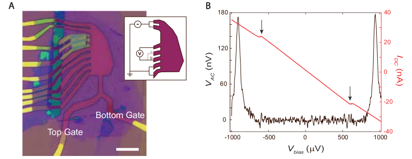
Transport measurements: Longitudinal resistance measurements are performed utilizing lock-in techniques at frequencies in the DC limit 48 Hz and low currents of 1 - 2 nA. Each transport line is filtered by several Pi- and RC-filter stages at the mixing chamber and an additional RC filter with a cutoff 5.7 kHz on the sample holder to reduce electronic noise and lower the electron temperature. We want to note that the present device has very long ( 10 m) dual gated bilayer graphene contact leads (sample image see S13A) - compared to the many layer graphite contacts of devices used in previous studies[14]. Thus, the contacts are in the same phase as the bulk of the sample which has two consequences: first, contact resistances are a higher than for many layer graphite contacts of similar aspect ratio, leading to additional heating at the contacts. We attribute the saturation of resistance of SC1 at the lowest temperatures to this heating effect (see Fig. 1D) while the disequilibration of the charge carriers with the phonon bath simultaneously prevents efficient cooling. Second, the contacts become superconducting at much lower critical currents (corresponding to similar current densities) due to their long aspect ratio. In Fig. S13B, raw data is shown taken at = -7.3 1011 cm-2, = 1.15 V/nm where of SC2 is maximal. The AC voltage drop across the sample and the DC current flowing through the sample is plotted against applied DC voltage bias. While the raw voltage drop follows typical behavior for a superconductor, the DC current shows two kinks without corresponding feature in the AC voltage data. These kinks can be explained by the superconducting transition of the dual gated bilayer graphene leads. As we calculate , such kinks visually imprint themselves onto the noise fluctuations of the zero resistance state—even in a four-terminal measurement setup. Therefore, features within the superconducting state such as in e.g. Fig. 2E or Fig. 4D should be disregarded as artefacts.
Shubnikov-de-Haas measurements: Magnetic field dependence of the longitudinal resistance of Fig. 2, S3 and S5 are taken with constant spacing in 1/ down to the lowest fields where quantum oscillation are visible. We perform Fourier transformations over different field ranges (see S4) sampled in and show the lowest field range in the main text for which all primary peaks of the quantum oscillations are clearly visible. This method reduces effects of higher harmonics and magnetic breakdown between different Fermi surfaces[40] (additional peaks in Fig. SS4C) and ensures that we can correlate our QO data with the zero field phase diagram.
Field dependence: All measurements are performed in a dilution refrigerator with base temperature of 10 - 20 mK and a 1T/1T/9T (XYZ) superconducting vector magnet. For the measurements of domes vs , the sample is mounted with the field of the Z magnet aligned to the bilayer graphene plane and the out-of plane field component is carefully minimized to be 0.1 mT using the XY magnets. is determined for discrete in-plane fields as flux trapping in the XY magnets and field misalignment of the Z magnet with the sample in this configuration prohibits continuous sweeping of while keeping 0.0 mT.
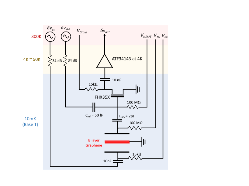
Penetration field capacitance: We utilize a capacitance bridge circuit to measure penetration field capacitance. In a previous capacitance bridge setup ([68]), a FHX35X high electron mobility transistor (HEMT) is directly connected to the sample gate, resulting in elevated electron temperatures above 100 mK. In order to lower the electronic temperature, we add an isolation capacitor made of silicon between the HEMT and the sample. We also installed a series of attenuators at each temperature stage to ensure thermalization of input coaxial cables. Finally, we added an ATF34143 HEMT at the 4K stage to transform the output impedance of the FHX35X HEMT and increase the bandwidth of output signal. (for full circuit schematic see Fig. reffig:S14).
We apply an A.C. excitation of 1 - 2 mV and a frequency of 166.667 kHz. The improved capacitance setup described above allows us to measure inverse compressibility at the base temperature of our dilution unit. This can be best seen in Fig. 4B where transport and capacitance are measured simultaneously. Superconductivity is well developed in this case. This indicates no significant increase in the electron temperature; as a reference, in BBG on hBN is less than 30mK. Indeed, linecuts with and without[14] simultaneous capacitance measurement show no noticeable difference.
II Band Structure Calculations
We computed the electronic dispersion and density of states of BBG with layer-specific Ising spin-orbit coupling at interlayer potential meV and electronic density . The band structure of bilayer graphene without spin-orbit coupling is well-described near the and points by a continuum model, expressed in the basis as [70, 36]
Here, Å is the monolayer graphene lattice constant and indicates whether has been expanded about the or valley. The hopping parameters are: = 3.16 eV for same layer hopping between nearest-neighbor sites, interlayer coupling term meV for same effective hopping between dimer sites and , interlayer coupling term meV for trigonal warping, and meV for interlayer coupling between the dimer and non-dimer sites [71, 70]. Adding monolayer WSe2 adjacent to one side of the bilayer graphene induces Ising SOC on the adjacent layer and can be accounted for in the model by adding a Hamiltonian [72]
acting on the and sublattices. Here, is a Pauli matrix acting on the spin subspace. The total Hamiltonian is then . The electron density at chemical potential and interlayer bias is computed by evaluating
where indexes the energy bands and runs over the regular grid of momenta on which we computed the electronic dispersion . The factor normalizes for grid spacing. The electron density in Fig. 1 was evaluated at temperature = 10 mK. The density of states is computed by grouping the energy eigenvalues in bins of equal width and normalizing by bin size to be consistent with .
III Additional Notes on the Competing Order State
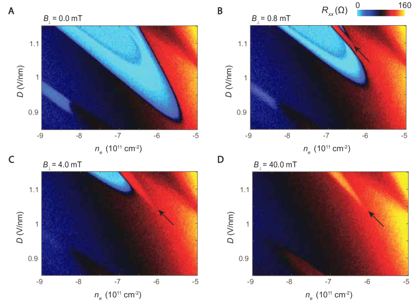
In the main text discussion of Fig. 3, we have noted a suppression of superconductivity at densities around -6.9 1011cm-2 and highest displacement fields. Here, additional data is shown in order to support and contextualize this argument and give further information about this ”competing order state” (COS). First, the location of the COS is shown in Fig. S10 — only developing at high above 1.05 V/nm for a small density range. A small out-of-plane magnetic field favors such state over SC2 as indicated by the black arrows. Fig. S9A-D displays temperature and dependence of SC2 at = 1.15 V/nm. Again, the COS appears at finite out-of-plane field and elevated temperatures with a characteristically increased resistance. It is useful to compare the energy scales of superconducting gap and depairing energy due to finite Cooper pair momentum. For a simple BCS superconductor, the superconducting gap is proportional to . An out-of-plane magnetic field breaks Cooper pairs due to their orbital motion at an energy that is proportional to . Thus, we contrast and plotted against density. Their density dependence agrees reasonably well within error, most notably in the region of the COS at -6.9 1011cm-2. Following this argument, not only , but the superconducting gap is suppressed at these densities. As the analysis of Ising superconductivity similarly assumes a superconducting gap proportional to temperature, the same conclusion can also be drawn from the quality of the curve collapse in Fig. 3B.
Non-linear transport reveals that COS is destroyed at finite current (Fig. S9E-G) with a critical temperature similar to of SC2, reminiscent of a charge density wave state. Interestingly, the balance between COS and SC2 is tipped in favor of superconductivity by lowering the magnetic field and temperature (Fig. S11). We also want to note that the fermiology evolves smoothly across COS (Fig. 2F) implying no additional symmetry breaking within the different isospin flavors. Instead, a natural explanation might involve nesting of different Fermi surfaces—only favored for wave vectors at specific densities.
IV Supplementary Figures
.

