Hardware implementation of quantum stabilizers in superconducting circuits
Abstract
Stabilizer operations are at the heart of quantum error correction and are typically implemented in software-controlled entangling gates and measurements of groups of qubits. Alternatively, qubits can be designed so that the Hamiltonian corresponds directly to a stabilizer for protecting quantum information. We demonstrate such a hardware implementation of stabilizers in a superconducting circuit composed of chains of -periodic Josephson elements. With local on-chip flux- and charge-biasing, we observe a progressive softening of the energy band dispersion with respect to flux as the number of frustrated plaquette elements is increased, in close agreement with our numerical modeling.
Protecting fragile information in quantum processors requires some form of quantum error correction (QEC). With typical “software” QEC techniques such as the surface code [1], stabilizing a single logical qubit requires many physical qubits, each of which is typically implemented as a weakly nonlinear oscillator. Error correction and computation is achieved by a string of operations and measurements that allow identification of bit-flip and phase-flip errors. An alternative is to implement quantum stabilizers directly in hardware. Here, error correction arises from the natural quantum dynamics, reducing the need for repeated entangling gates, measurements, and a multitude of control lines and complex classical control hardware. In this approach, the highly non-trivial Hamiltonian results in a tiny protected subspace within a huge Hilbert space.
Both approaches can be characterized by the error suppression factor , the rate at which the logical error decreases with system size. The long time required by each round of software error correction for current transmon qubit arrays implies that is only marginally greater than one [2]. In this work, we experimentally demonstrate the potential to achieve much larger 100 with the Hamiltonian approach. The price that one pays is the appearance of relatively low energy modes with gaps that make initialization challenging; these gaps can be made higher through parameter optimization. Before building a scalable logical qubit with hardware QEC, it is crucial to demonstrate the effectiveness of protection based on Hamiltonian engineering as system size increases. In this manuscript, we observe and quantify the stabilizing interaction Hamiltonian between unprotected elements. We perform spectroscopic measurements with local flux control and observe signatures of stabilizer terms in the Hamiltonian. Specifically, we find a progressive flattening of the energy bands with respect to flux as system size increases, consistent with linear flux dispersion for a system size of one, quadratic for two, and cubic for three. In addition, we observe a characteristic periodic modulation with offset charge as we tune between regimes with different levels of protection.
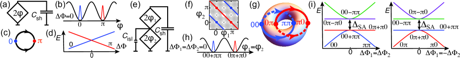
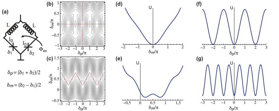
A variety of qubit designs with intrinsic protection against decoherence have been studied previously [3, 4], including the 0 qubit [5, 6, 7], the two-Cooper-pair tunneling qubit [8], the bifluxon qubit [9], and rhombi arrays [10, 11, 12]. In this last work, previous devices had limited symmetry due to the inability to tune each element to the optimum flux independently; in addition, the devices were sensitive to offset charge fluctuations on internal nodes in each element, and the suppression of tunneling between the logical states was limited. Similar to previous protected qubit designs, our device is based on -periodic Josephson elements [13], for which the Josephson energy is proportional to , where is the superconducting phase difference across the element. Here, charge transport consists of coherent tunneling of , as opposed to for a conventional junction. We implement each element as a plaquette formed from a dc Superconducting QUantum Interference Device (SQUID), consisting of two conventional Josephson junctions and a non-negligible loop inductance. When flux-biased at frustration, (), the first harmonic of the Josephson energy (proportional to ) vanishes. This leaves a second order term , with sequential minima separated by ; depends on the Josephson energy of the individual junctions and the energy of the SQUID inductance (Supplement [14], Sec. XI); is thus a compact variable residing on a circle. Biasing below (above) raises (lowers) the wells relative to the wells; for flux bias at 0, the potential becomes proportional to . A small asymmetry between the two junctions has a similar but less severe effect on the potential compared to a small flux deviation from frustration (Supplement [14], Sec. I).
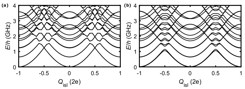
For a single frustrated plaquette with a large capacitive shunt [Fig. 1(a)], tunneling between the ground states in the wells is suppressed. In the phase basis, wavefunctions localized in the wells are thus disjoint and well protected against bit-flip errors. At the same time, the wavefunctions are spread out in the charge basis, corresponding for the 0() states to superpositions of even (odd) multiples of Cooper pairs on the logical island where the plaquette connects to . For bias away from frustration, the energy levels disperse linearly [Fig. 1(d)], with no protection against phase flips due to flux noise.
We next consider concatenation of multiple plaquettes while maintaining the large shunt across the array. At double frustration, when two plaquettes are simultaneously biased to , there are four minima in the two-dimensional surface defined by the phase drops across each plaquette: . For the two-plaquette circuit this has the topology of a torus, since for each plaquette is a compact variable with periodicity [Fig. 1(f,g)]. If the capacitance of the intermediate island between plaquettes to ground is sufficiently small, with charging energy , quantum fluctuations of the island phase cause hybridization along the direction between wells of the same parity; that is, will hybridize with and with . Levels with the same parity develop a splitting near double frustration, with ground states corresponding to the symmetric superpositions () for even (odd) parity. Excited states are given by the antisymmetric superpositions 00- (-) for even (odd) parity; these states are separated by an energy from the symmetric ground state of the same parity. The hybridized ground state wavefunctions of opposite parity are the logical states for the device [Fig. 1(h)] and form interlocking rings on the torus [Fig. 1(g)]. Due to delocalization and intertwining of the hybridized ground state wavefunctions, local perturbations affect the logical states symmetrically. Larger increases and further flattens the bands [Fig. 1(i)], thus protecting against dephasing from flux noise.
Treating each plaquette as a spin-1/2 particle, the splitting corresponds to an stabilizer term in the Hamiltonian of frustrated plaquettes : , where is the Pauli matrix for plaquette . The error suppression factor can be approximated as the ratio of to twice the scale of dephasing fluctuations for single plaquette , , which, for this device, will be dominated by flux noise (Supplement [14], Sec. XII). still suppresses tunneling between logical states of opposite parity, protecting against bit-flip errors.
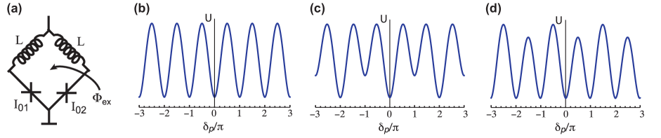
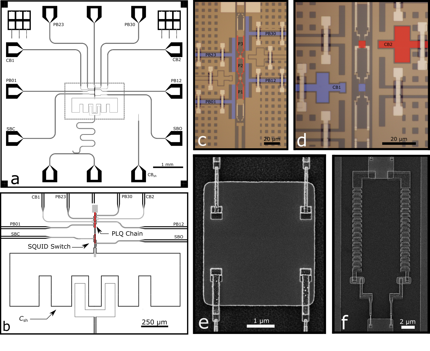
In our experiments, we target a three-plaquette circuit with (=1), where is the energy of the inductance on each plaquette arm. We aim for a charging energy of each plaquette junction , where is the junction capacitance. These values can be achieved with conventional Al-AlOx-Al junctions. We implement the inductors with chains of large-area junctions, similar to fluxonium [17], thus eliminating charge fluctuations on the internal nodes between each small junction and inductor within a plaquette. The shunt capacitor =1.2 pF is capacitively coupled to a resonator. There are four flux-bias lines, each of which couples strongly to one or two plaquettes. There are three charge-bias lines: one to the logical island that forms , and one to each intermediate island between plaquettes (Supplement [14], Sec. II-V).
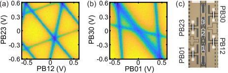
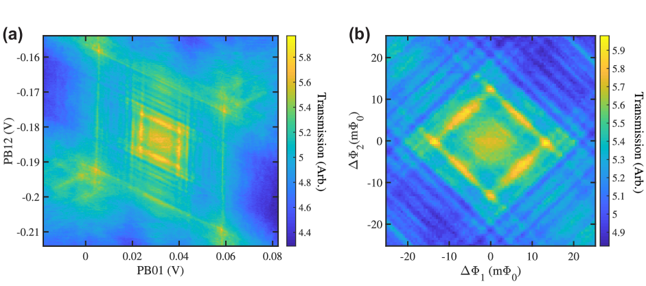
For device tune-up, we scan various pairs of flux-bias lines while monitoring the dispersive shift of the readout resonator. Each blue line in Fig. 2(a,b) corresponds to one plaquette passing through frustration. A crossing of two (three) lines indicates double (triple) frustration. The spacing between parallel sets of lines defines the period . We fit the slopes and spacing of the lines to extract the inductance matrix mapping bias levels on each flux line to net flux coupled to each plaquette (Supplement [14], Sec. VI). By inverting this matrix, we determine bias parameters for moving along arbitrary flux vectors.
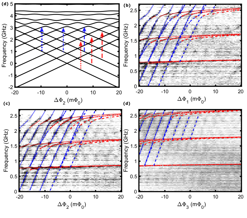
We next map out the flux dispersion of the level transitions for different frustration conditions. With our ability to adjust the various plaquette fluxes independently using local flux-biasing, we maintain some plaquettes at unfrustration (0), where the plaquette behaves like a conventional Josephson element, while we scan the flux of other plaquettes near frustration. In Fig. 3, we consider the expected level structure and define the types of possible transitions. We refer to transitions between levels in the same well as plasmons; transitions between different wells are referred to as heavy fluxons because of the vanishingly small gap associated with the corresponding anticrossing, a consequence of the large effective mass from . Transitions between hybridized levels of the same parity but opposite symmetry, for example, + to -, disperse sharply with flux; these are known as light fluxons due to the low effective mass in the direction from the smallness of .
To perform spectroscopy, we drive a microwave probe tone into the charge bias line coupled to while monitoring the cavity dispersive shift. Near single frustration, we initialize in the well prior to each spectroscopy pulse by setting the bias to from frustration, thus moving out of the protected space; we then quickly ramp the bias to the measurement point and apply spectroscopy and readout pulses (Supplement [14], Sec. VII). In Fig. 4(a), we show single-frustration measurements for plaquette 2. Features that disperse gradually correspond to plasmons within the well where the qubit is initialized. We continue to observe transitions out of the well even when the device is biased past frustration, where the well is higher in energy than the 0 well, due to suppressed tunneling between states of opposite parity. In addition to the 0-1, 0-2, and 0-3 transitions, we observe transitions out of excited states in the well, such as 1-2, 1-3, and 1-4, and even 2-3 and 2-4, due to insufficient cooling into the ground state of the well. Because of the spurious excitations to multiple levels, we are unable to apply initialization techniques that are commonly used for other low-gap qubits, such as heavy fluxonium [31, 32]. Nevertheless, we observe only weak transitions out of the 0 well, indicating that we are predominantly preparing the circuit in the well. In addition to the plasmons, we also observe heavy fluxons that disperse linearly with flux, which arise from transitions between various levels in the and 0 wells, where the barrier to tunneling is small because the initial state is an excited level or the wells are tilted by the flux bias; note that we do not observe the heavy fluxon between the protected ground states in the 0 and wells, which are the logical levels. We observe similar behavior for plaquettes 1 and 3 (Supplement [14], Sec. X).
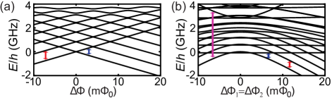
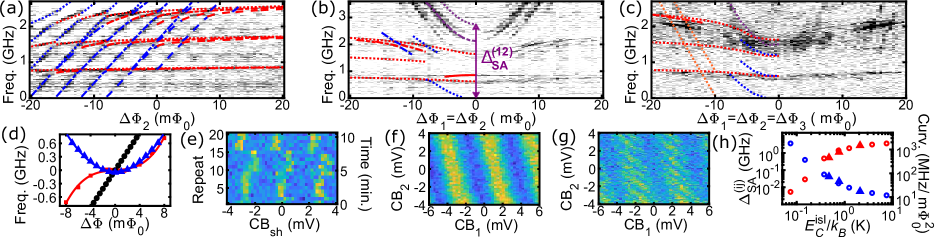
The curves included in Fig. 4(a) are generated from detailed numerical modeling of the device energy levels (Supplement [14], Sec. IX). With the ability to calculate the level spectrum, we adjust the circuit parameters to fit the measured transitions from the spectroscopic data (Supplement [14], Sec. X). We observe excellent agreement, even capturing splittings that result when a fluxon crosses a plasmon due to resonant tunnel coupling between aligned levels in the 0 and wells. In addition, these splittings depend on the offset charge on the island [Fig. 4(e)] due to Aharonov-Casher (A-C) interference [33, 34] between tunneling paths clockwise (CW) or counterclockwise (CCW) in the potential [Fig. 1(c)] (Supplement [14], Sec. VIII). At single frustration, as expected, the heavy fluxon dispersion is linear down to zero energy, thus offering no protection against flux noise.
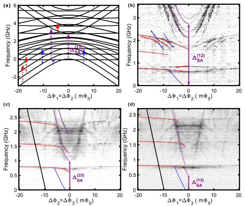
Upon tuning to double frustration, we observe a qualitatively different behavior. We initialize in the well of the two-plaquette potential, then quickly ramp near double frustration. We scan both plaquette fluxes in tandem along the direction between the regimes with a global potential minimum at and 00 and passing through double frustration. Spectroscopy at plaquette (12) double frustration shows plasmons similar to the single frustration measurements [Fig. 4(b)]. However, unlike single frustration, where suppressed tunneling between the wells allows the device to remain in the well even after the flux is ramped well past frustration, at double frustration, the large symmetric-antisymmetric gap causes an adiabatic transition from to 00 upon passing through double frustration. At higher frequencies, we observe steeply dispersing light fluxons, with the minimum at double frustration corresponding to from hybridization of the 00 and wells. For scans along the odd-parity flux direction, or if the circuit is initialized in an odd-parity well and scanned in the even-parity flux direction, the spectral features become swapped [Fig. 1(i), Supplement [14], Sec. X.C].
As with spectroscopy at single frustration, we include curves for the various transitions from numerical modeling and fitting for double frustration [Fig. 4(b)]. Here, the larger Hilbert space requires a significant increase in computational resources. Our modeled transition curves agree well with the measured spectroscopy, capturing both the plasmons and heavy fluxons. We are unable to directly drive a microwave transition between the logical states in the + and + wells due to the vanishing matrix element, the basis of protection. However, the increasing flatness of the higher fluxon transitions as one moves lower in the spectrum indicates that the logical levels will be the flattest. This can also be seen in the blue modeled curves near the bottom of the figure highlighting the dispersion of the logical level transition, which exhibits quadratic curvature. Additionally, our modeling captures the light fluxons to the antisymmetric levels.
The effectiveness of concatenation depends on of the intermediate island between the two frustrated plaquettes. For plaquette (12) double frustration, is 2.7 GHz. At plaquette (23) double frustration, which involves a significantly larger because of the orientation of the plaquette 2 inductors, we observe a smaller and a correspondingly larger curvature of the heavy fluxon transition. is even smaller because of the excess capacitance to ground of the unfrustrated plaquette 2 (Supplement [14], Sec. X). Figure 4(h) shows the variation of with , including measured values of for each combination of double frustration, as well as numerically modeled values. For a typical flux noise level, for these plaquettes will be 2 MHz, which, when combined with the measured , is consistent with . Note that this is an extracted parameter characterizing protection in one channel: dephasing. The complete -parameter for a logical qubit must be derived from the scaling of and with system size, which is beyond the scope of this manuscript. Nonetheless, can also be expressed as the ratio of for a higher degree of frustration relative to at single frustration (Supplement [14], Sec. XII).
In addition to the symmetric/antisymmetric gap, another characteristic of the stabilizer term is the periodic modulation of with offset charge on the intermediate island between plaquettes and . Destructive A-C interference of tunneling paths in the CW and CCW directions on the constant-parity circles for double frustration [Fig. 1(g)] causes to vanish for island offset charge near . We observe periodic modulation with charge bias to the islands with a spectroscopy pulse on the 0-1 transition [Fig. 4(f)]. While the island offset charge is stable on timescales up to one hour, it is critical there are no jumps to near . Thus, it is important to actively stabilize these offset charges through periodic calibrations (Supplement [14], Sec. VIII, IX).
By simultaneously frustrating all plaquettes, we measure spectroscopy near triple frustration [Fig. 4(c)]. In this case, we are unable to numerically fit the level spectrum since the Hilbert space size becomes prohibitively large. Nonetheless, we are able to compute the spectrum using parameter values from previous fits to double and single frustration, although the calculation takes several weeks to complete. We obtain reasonable agreement with the measurements, although the spectral features are more challenging to resolve compared to other degrees of frustration; the higher transitions are off by 5-10%, which is not unreasonable considering the circuit complexity and intertwined wavefunctions, given limitations on the number of quantum states needed for the computation to converge. Around 1.5 GHz, we observe a prominent central flat feature of width 7 m around the 0-3 transition, which is uncharacteristic for parabolic, let alone linear, dispersion; below this, the 0-1 transition around 0.6 GHz is similarly flat. The transition between the logical states, which cannot be directly driven due to protection of these states from the environment, will be comparably flat (Supplement [14], Sec. X.D). Also, the light fluxon transitions are qualitatively different compared to double frustration. We additionally observe charge modulation with two different periods and slopes corresponding to separate tuning of offset charge on each intermediate island [Fig. 4(g)], characteristic of a Hamiltonian with two stabilizer terms: . For our present device is smaller than due to excess ground capacitance from plaquette 2, resulting in the logical level dispersion at triple frustration being only marginally flatter than at double frustration [Fig. 4(d)] (Supplement [14], Sec. XI).
While our present device successfully demonstrates the implementation of stabilizer terms in hardware, development of protected qubits based on hybridized ground states of opposite parity requires larger gaps to the excited states. This, in conjunction with weaker radiative coupling to parasitic high-frequency modes from a more compact , perhaps achieved using a parallel-plate rather than planar design, will avoid spurious excitations to multiple excited levels that complicate the initialization process for our present device. A device with higher excited-state energies that can be operated in the qubit regime requires larger , ideally at least 3 K. We must also maintain even larger to have large at double frustration with the resulting flat dispersion. For a qubit with these improved parameters subject to typical flux- and charge-noise levels, optimistic but feasible junction asymmetries, and dielectric loss from a parallel-plate , we project 100, corresponding to and (Supplement [14], Sec. XI), well beyond current state-of-the-art superconducting qubits.
This work is supported by the U.S. Government under ARO grant W911NF-18-1-0106. Fabrication was performed in part at the Cornell NanoScale Facility, a member of the National Nanotechnology Coordinated Infrastructure (NNCI), which is supported by the National Science Foundation (Grant NNCI-2025233). Portions of this work were supported by the National Science Foundation, Quantum Leap Challenge Institute for Hybrid Quantum Architectures and Networks, Grant No. 2016136.
References
- Fowler et al. [2012] A. G. Fowler, M. Mariantoni, J. M. Martinis, and A. N. Cleland, Surface codes: Towards practical large-scale quantum computation, Physical Review A 86, 032324 (2012).
- Google Quantum AI [2021] Google Quantum AI, Exponential suppression of bit or phase errors with cyclic error correction, Nature 595, 383 (2021).
- Douçot and Ioffe [2012] B. Douçot and L. B. Ioffe, Physical implementation of protected qubits, Reports on Progress in Physics 75, 072001 (2012).
- Gyenis et al. [2021a] A. Gyenis, A. Di Paolo, J. Koch, A. Blais, A. A. Houck, and D. I. Schuster, Moving beyond the Transmon: Noise-Protected Superconducting Quantum Circuits, PRX Quantum 2, 030101 (2021a).
- Brooks et al. [2013] P. Brooks, A. Kitaev, and J. Preskill, Protected gates for superconducting qubits, Phys. Rev. A 87, 052306 (2013).
- Groszkowski et al. [2018] P. Groszkowski, A. Di Paolo, A. Grimsmo, A. Blais, D. I. Schuster, A. A. Houck, and J. Koch, Coherence properties of the 0- qubit, New Journal of Physics 20, 043053 (2018).
- Gyenis et al. [2021b] A. Gyenis, P. S. Mundada, A. Di Paolo, T. M. Hazard, X. You, D. I. Schuster, J. Koch, A. Blais, and A. A. Houck, Experimental Realization of a Protected Superconducting Circuit Derived from the 0– Qubit, PRX Quantum 2, 010339 (2021b).
- Smith et al. [2020] W. C. Smith, A. Kou, X. Xiao, U. Vool, and M. H. Devoret, Superconducting circuit protected by two-Cooper-pair tunneling, npj Quantum Information 6, 8 (2020).
- Kalashnikov et al. [2020] K. Kalashnikov, W. T. Hsieh, W. Zhang, W.-S. Lu, P. Kamenov, A. Di Paolo, A. Blais, M. E. Gershenson, and M. T. Bell, Bifluxon: Fluxon-Parity-Protected Superconducting Qubit, PRX Quantum 1, 010307 (2020).
- Ioffe et al. [2002] L. B. Ioffe, M. V. Feigel’man, A. Ioselevich, D. Ivanov, M. Troyer, and G. Blatter, Topologically protected quantum bits using Josephson junction arrays, Nature 415, 503 (2002).
- Gladchenko et al. [2009] S. Gladchenko, D. Olaya, E. Dupont-Ferrier, B. Douçot, L. B. Ioffe, and M. E. Gershenson, Superconducting nanocircuits for topologically protected qubits, Nature Physics 5, 48 (2009).
- Bell et al. [2014] M. T. Bell, J. Paramanandam, L. B. Ioffe, and M. E. Gershenson, Protected Josephson Rhombus Chains, Physical Review Letters 112, 167001 (2014).
- Smith et al. [2022] W. C. Smith, M. Villiers, A. Marquet, J. Palomo, M. R. Delbecq, T. Kontos, P. Campagne-Ibarcq, B. Douçot, and Z. Leghtas, Magnifying Quantum Phase Fluctuations with Cooper-Pair Pairing, Physical Review X 12, 021002 (2022).
- [14] See Supplemental Material for further details of the device design, fabrication, measurements, data analysis, and numerical modeling, which includes Refs. [15, 16, 17, 18, 19, 20, 21, 22, 23, 24, 25, 26, 27, 28, 29, 30].
- Lefevre-Seguin et al. [1992] V. Lefevre-Seguin, E. Turlot, C. Urbina, D. Esteve, and M. H. Devoret, Thermal activation of a hysteretic dc superconducting quantum interference device from its different zero-voltage states, Physical Review B 46, 5507 (1992).
- Mooij et al. [1999] J. Mooij, T. Orlando, L. Levitov, L. Tian, C. H. Van der Wal, and S. Lloyd, Josephson Persistent-Current Qubit, Science 285, 1036 (1999).
- Manucharyan et al. [2009] V. E. Manucharyan, J. Koch, L. I. Glazman, and M. H. Devoret, Fluxonium: Single Cooper-Pair Circuit Free of Charge Offsets, Science 326, 113 (2009).
- Koch et al. [2007] J. Koch, T. M. Yu, J. Gambetta, A. A. Houck, D. I. Schuster, J. Majer, A. Blais, M. H. Devoret, S. M. Girvin, and R. J. Schoelkopf, Charge-insensitive qubit design derived from the Cooper pair box, Physical Review A 76, 042319 (2007).
- Eckern et al. [1984] U. Eckern, G. Schön, and V. Ambegaokar, Quantum dynamics of a superconducting tunnel junction, Physical Review B 30, 6419 (1984).
- [20] InductEx, SUN Magnetics.
- Foxen et al. [2018] B. Foxen, J. Mutus, E. Lucero, E. Jeffrey, D. Sank, R. Barends, K. Arya, B. Burkett, Y. Chen, Z. Chen, et al., High speed flux sampling for tunable superconducting qubits with an embedded cryogenic transducer, Superconductor Science and Technology 32, 015012 (2018).
- Rol et al. [2020] M. A. Rol, L. Ciorciaro, F. K. Malinowski, B. M. Tarasinski, R. E. Sagastizabal, C. C. Bultink, Y. Salathe, N. Haandbæk, J. Sedivy, and L. DiCarlo, Time-domain characterization and correction of on-chip distortion of control pulses in a quantum processor, Applied Physics Letters 116, 054001 (2020).
- [23] ANSYS, ANSYS Q3D Extractor.
- Christensen et al. [2019] B. G. Christensen, C. D. Wilen, A. Opremcak, J. Nelson, F. Schlenker, C. H. Zimonick, L. Faoro, L. B. Ioffe, Y. J. Rosen, J. L. DuBois, B. L. T. Plourde, R. McDermott, Anomalous charge noise in superconducting qubits, Physical Review B 100, 140503(R) (2019).
- Wilen et al. [2021] C. Wilen, S. Abdullah, N. Kurinsky, C. Stanford, L. Cardani, G. d’Imperio, C. Tomei, L. Faoro, L. Ioffe, C. Liu, et al., Correlated charge noise and relaxation errors in superconducting qubits, Nature 594, 369 (2021).
- Rafferty et al. [2021] O. Rafferty, S. Patel, C. Liu, S. Abdullah, C. Wilen, D. Harrison, and R. McDermott, Spurious Antenna Modes of the Transmon Qubit, arXiv preprint arXiv:2103.06803 (2021).
- Liu et al. [2022] C.-H. Liu, D. C. Harrison, S. Patel, C. D. Wilen, O. Rafferty, A. Shearrow, A. Ballard, V. Iaia, J. Ku, B. Plourde, et al., Quasiparticle Poisoning of Superconducting Qubits from Resonant Absorption of Pair-breaking Photons, arXiv preprint arXiv:2203.06577 (2022).
- Klots [2022] A. R. Klots, SuperQuantPackageV2 (2022), [Online; accessed 6. Jul. 2022], URL https://github.com/andreyklots/SuperQuantPackageV2.
- O’Connell et al. [2008] A. D. O’Connell, M. Ansmann, R. C. Bialczak, M. Hofheinz, N. Katz, E. Lucero, C. McKenney, M. Neeley, H. Wang, E. M. Weig, et al., Microwave dielectric loss at single photon energies and millikelvin temperatures, Appl. Phys. Lett. 92, 112903 (2008), ISSN 0003-6951.
- Astafiev et al. [2006] O. Astafiev, Y. A. Pashkin, Y. Nakamura, T. Yamamoto, and J.-S. Tsai, Temperature Square Dependence of the Low Frequency Charge Noise in the Josephson Junction Qubits, Physical Review Letters 96, 137001 (2006).
- Gusenkova et al. [2021] D. Gusenkova, M. Spiecker, R. Gebauer, M. Willsch, D. Willsch, F. Valenti, N. Karcher, L. Grünhaupt, I. Takmakov, P. Winkel, et al., Quantum Nondemolition Dispersive Readout of a Superconducting Artificial Atom Using Large Photon Numbers, Physical Review Applied 15, 064030 (2021).
- Vool et al. [2018] U. Vool, A. Kou, W. C. Smith, N. E. Frattini, K. Serniak, P. Reinhold, I. M. Pop, S. Shankar, L. Frunzio, S. M. Girvin, and M. H. Devoret, Driving Forbidden Transitions in the Fluxonium Artificial Atom, Physical Review Applied 9, 054046 (2018).
- Aharonov and Casher [1984] Y. Aharonov and A. Casher, Topological Quantum Effects for Neutral Particles, Physical Review Letters 53, 319 (1984).
- Bell et al. [2016] M. T. Bell, W. Zhang, L. B. Ioffe, and M. E. Gershenson, Spectroscopic Evidence of the Aharonov-Casher Effect in a Cooper Pair Box, Physical Review Letters 116, 107002 (2016).
Supplementary Information: Hardware implementation of quantum stabilizers in superconducting circuits
I. -periodic Josephson elements from dc SQUIDs
In our device, we implement each -periodic Josephson element with a plaquette formed from a dc Superconducting QUantum Interference Device (SQUID), consisting of two conventional Josephson junctions and a non-negligible loop inductance [Fig. S1(a)]. Each junction has a critical current and ; the inductance in each arm of the SQUID is related to the inductive energy . In order to understand the origin of the potential, we consider the two-dimensional potential energy landscape as a function of the two junction phases, and , which is determined by , , and the external flux bias [1]. For now, we consider symmetric plaquettes where both junction critical currents are identical; later in this section we will consider the effects of junction asymmetry. Following convention for dc SQUIDs we plot the potential energy in terms of the common-mode and differential phase variables: and . The phase dependence of the Josephson energy for each junction results in a 2D washboard pattern of potential minima. At the same time, the inductive energy associated with circulating currents flowing through the inductors corresponds to a parabolic sheet with its minimum along a line running parallel to . Changing shifts where the minimum of this inductive parabolic sheet falls with respect to the minima of the Josephson washboard, and thus determines the pattern of the global minima in the potential.
For a flux bias at unfrustration , the minima are centered on and are spaced by in [Fig. S1(b)]. Along , there is only the one minimum at [Fig. S1(d)], corresponding to no circulating current around the SQUID loop. Along for , the potential follows a dependence. Thus, at unfrustration, the plaquette behaves like a single Josephson junction with critical current . When flux biased at , the plaquette exhibits a staggered pattern of energy minima about a line along for [Fig. S1(c)]. Figure S1(e) shows a linecut along a line between two adjacent minima as a function of ; the two minima correspond to opposite senses of circulating current around the plaquette loop, similar to a flux qubit [2] or fluxonium [3]. However, unlike these other qubits, these plaquettes also have another independent phase degree of freedom from , which corresponds to the phase drop across the plaquette. Along , the potential is simply , with sequential minima separated by [Fig. S1(g)], where the energy scale depends on the Josephson energies of the individual Josephson junctions and the inductive energy of the SQUID loop inductance .
While the behavior described here is generic for any dc SQUID, achieving a potential at frustration with a significant barrier height requires a sufficiently large ratio . In the conventional language of dc SQUIDs, screening effects are characterized by the parameter . For SQUIDs in the limit and perfect symmetry, the critical current of the SQUID will modulate to zero at frustration. For such a device, not only is the first-order Josephson energy suppressed, but will be vanishingly small as well, and thus not support bound states in a potential. In order to have a significant , must be of order unity. The dc SQUID in Fig. S1 has to highlight the development of the -periodicity at frustration.
We next consider deviations from this ideal -periodic plaquette behavior. With the flux bias moved below (above) frustration (), the wells are raised above (below) the wells [Fig. S2(c)]. To account for asymmetries between the two junctions in a plaquette we define , where is the Josephson energy of the left (right) junction. With a non-zero , the common-mode potential along for has equal minima for the 0 and wells, but now the barrier heights between wells become asymmetric.
II. Device Fabrication
This device was fabricated on a high resistivity (10 k-cm) silicon wafer that was given a standard RCA clean followed by an etch step in a buffered-2% per volume HF bath to remove native oxides immediately before loading into a vacuum chamber for the base-layer metal deposition. The base layer of 60-nm thick niobium is sputter-deposited and is then coated with DSK101-4 anti-reflective-coating (ARC) and DUV210-0.6 photoresist before performing deep-UV photolithography on a photostepper to define the ground plane, feedline, resonator, flux/charge bias lines, and the logical islands. The exposed wafer is then baked at 135∘C for 90 seconds, developed with AZ 726 MiF, briefly cleaned with an ARC etch to remove any remaining unwanted ARC and then dry etched using a BCl3, Cl2, and Ar in an inductively coupled plasma etcher. The wafer is then subject to another buffered HF dip to remove any further oxides that may have formed on the surface of the remaining niobium.
The next set of lithography steps creates ground straps that connect ground planes on either side of the flux, charge, and feedlines. The first step uses lift-off resist LOR3A and then DUV210-0.6 photoresist to expose a region underneath the intended ground straps where we deposit SiO2 to function as an insulating dielectric support for the aluminum ground straps to follow. The SiO2 is evaporated in an electron beam evaporator at a rate 3.5 /s until 100 nm is deposited. The wafer is then placed in 1165 Remover (N-Methly-2-pyrrolidone (NMP)) at 65∘C to lift off the excess SiO2 and resist and then another clean bath of NMP at 65∘C for further liftoff. The wafer is then sonicated for 10 seconds to remove any final remaining resist and SiO2. The second layer of the ground strap process is exposed in the same way, using LOR3A and DUV photoresist, but this time the pattern lies over the existing SiO2 and extends further so that once developed, there is an exposed region of the niobium ground plane for the aluminum to contact. The wafer is baked again and developed, and the ground straps are then deposited by electron beam evaporation of aluminum (100 nm thick). The wafer is once again subject to NMP to remove the remaining resist and excess aluminum.
Once clean, the wafer is put through a light oxygen plasma resist strip before a bilayer resist stack of MMA/PMMA is spun for electron beam lithography to define the Josephson junctions. The Al-AlOx-Al junctions are written at 100 keV to form a standard double-angle evaporation airbridge pattern. Following development, there is a brief ion mill step before the first electrode is deposited by electron beam evaporation. The bottom (top) electrode is 40 (80) nm thick. Once the junctions are deposited, the wafer is covered in S1813 photoresist and then diced to (6.25 mm)2 chips. After the dicing, the aluminum metallization is lifted off and the chips are then cleaned with a UV/ozone process before measurement.
III. Device Layout
In order to allow for local flux-biasing of the different plaquettes and charge-biasing of the various superconducting islands, our device incorporates a series of on-chip bias lines, indicated in Fig. S3. The heart of the device contains a chain of three plaquettes, each with two small Josephson junctions (130 nm 110 nm) and two junction-chain inductors (seventeen 140 nm 1070 nm junctions in series). As discussed in the main paper, minimizing for each intermediate island between two adjacent plaquettes is critical for successful concatenation. Thus, ideally the four Josephson junctions in two adjacent plaquettes will all be located near the island between the plaquettes so that the junction electrode that is closest to the island will be as short as possible and contribute a minimal amount of excess capacitance to ground. However, in a chain of three plaquettes, this is only possible for one of the two intermediate islands. The other island will necessarily have to be connected to the two inductors for one of the plaquettes, and the capacitance to ground for these inductors will enhance the effective island capacitance. In addition, the 3-plaquette chain has dummy plaquettes at either end, which have the same geometry as the other plaquettes, but the small junctions and inductor-chain junctions are intentionally shorted out. The dummy plaquettes are included to symmetrize the geometry and minimize the inductive coupling of the on-chip flux-bias lines to the mode of oscillation of the plaquette chain, sometimes referred to as the coupling, as defined in Ref. [4].
There are four on-chip flux-bias lines for controlling the flux bias to each of the three plaquettes, with the labeling as described in the main paper. Each flux-bias line has a coplanar geometry and splits into a T-shaped path adjacent to the plaquette chain, with the two ends of the T connected directly to the ground plane. In order to have a well-defined path for the return currents, and to suppress slot-line modes between different portions of the ground plane, we fabricated superconducting ground straps across each flux-bias line in multiple locations. In addition to the flux-bias lines, we also have three charge-bias lines for tuning the offset charge to the shunt capacitor electrode and each of the two intermediate islands between pairs of plaquettes. These charge-bias lines are isolated from ground, but also include similar ground straps to the flux-bias lines.
Our design also includes a pair of series dc SQUIDs between the plaquette chain and that could be used for gate operations in a future implementation of a protected qubit based on concatenated -periodic plaquettes. For the experiments presented here, this SQUID switch, which has separate flux-bias lines from the plaquettes, was not used and the two loops of the SQUID switch were maintained at a flux bias of 0 throughout the experiment. At this bias point, the SQUIDs behave primarily as superconducting shorts, although we must still account for the nonlinearity of the SQUID junctions in modeling the energy levels for our device.
The target shunt capacitance, for our present device is rather large compared to more conventional superconducting qubits. Nonetheless, in the present experiment, we implemented with a planar superconducting Nb electrode with a small gap to the ground plane around the perimeter. For measuring our device, we have a coplanar waveguide (CPW) readout resonator with a fundamental resonance at 4.7 GHz. This is a 1/4-wave resonator with one end inductively coupled to a CPW feedline that is connected to our measurement circuitry; the other end of the resonator has a coupling capacitance to our device.
The majority of our device is patterned in Nb, including the ground plane, bias lines, readout resonator, and shunt capacacitor. All Josephson junctions are fabricated from a standard Al-AlOx-Al double-angle shadow-evaporation process. As an initial attempt at superconductor gap engineering for reducing quasiparticle poisoning of the plaquette chain, we include two patches of Al for suppressing the Nb gap underneath – one patch is at the joint between the plaquette chain and the ground plane; the other patch is between the plaquette chain and shunt capacitor.
IV. Device and Measurement Setup
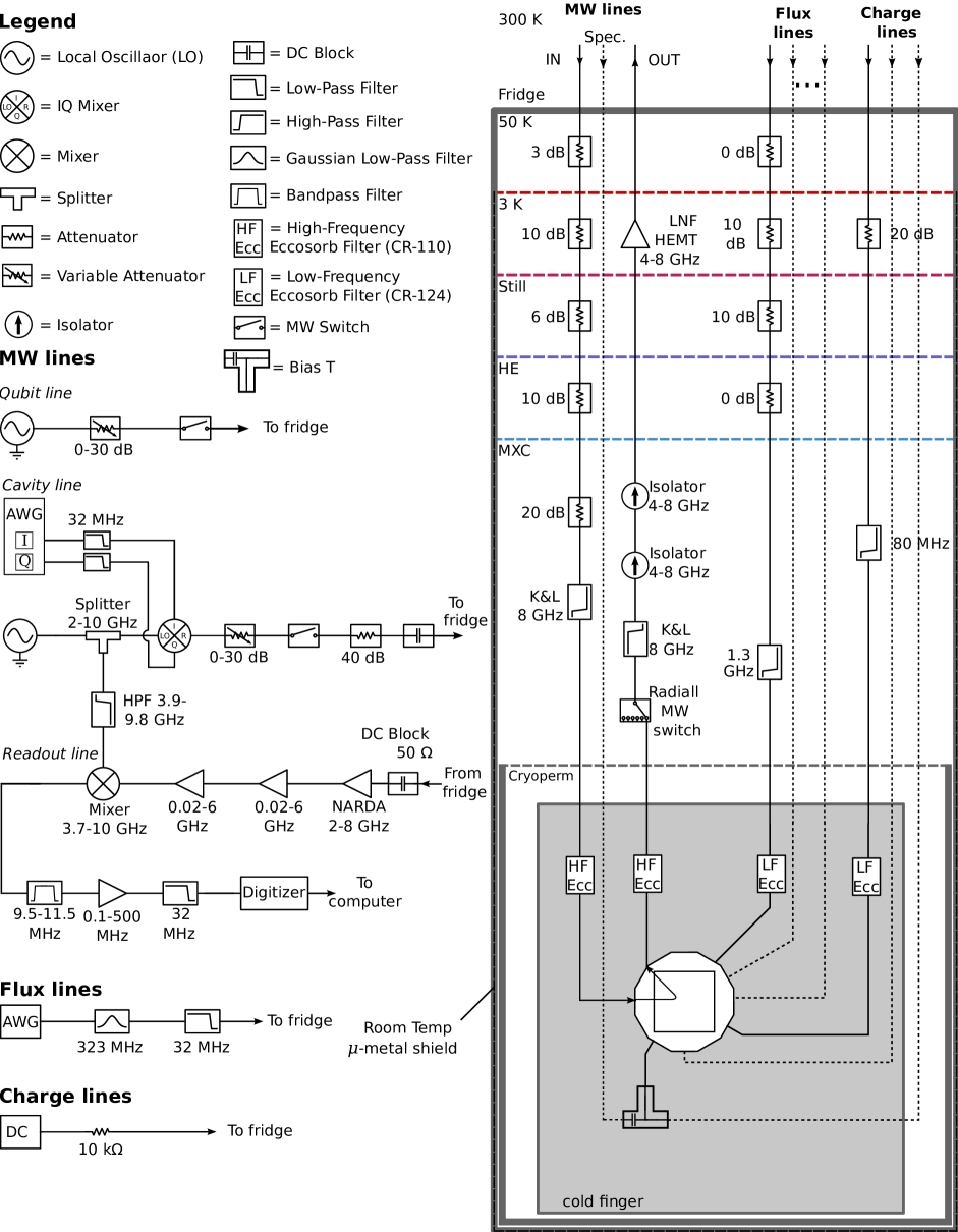
Measurements are performed on a cryogen-free dilution refrigerator running at a temperature below 15 mK. The device chip is wire-bonded into a machined Al sample box that is mounted on a cold-finger attached to the mixing chamber stage and surrounded by a Cryoperm magnetic shield. The detailed configuration of our cabling, attenuation, filtering, and shielding inside the refrigerator, and the room-temperature electronics hardware for control and readout, is shown in Fig. S4.
V. Device Parameters
Establishing clear stabilizer behavior at double frustration requires plaquettes with a dominant -periodic potential and large quantum fluctuations in the direction of constant + in the space of common-mode phases across each plaquette. The -periodicity comes from a dc SQUID consisting of two conventional Josephson junctions and a non-negligible loop inductance. We implement inductors in each plaquette with chains of large-area Josephson junctions, similar to typical fluxonium designs [3]. The inductive energy of the junction chain can be extracted with , where is the junction chain resistance at room temperature. To have large quantum fluctuations in the direction of constant for effective hybridization between the two plaquettes, we need large and compared to the barrier height, which determines the coupling between the 00 and wells and the 0 and 0 wells. For our device, we target , and (). For a junction with large and , if the junction plasma frequency approaches of the junction electrodes, the junction acquires an extra capacitance from quasiparticles on either side of the junction. This specific electronic capacitance can be expressed as [5], where is the critical current density of the junction and is the superconducting gap. Our target is 1.5 K and junction area is , and the corresponding 4 and fF. Our estimated specific geometric capacitance is 50 fF/, so fF. The total capacitance of the junction is fF, and 4 K. Junctions of this size are close to the lower limit where we can maintain reasonably small junction asymmetry with our fabrication. Thus, making smaller junctions to reduce is not practical. The simulated geometric charging energy of each intermediate island to ground is for the island between plaquettes 1 and 2, and for the island between plaquettes 2 and 3. The is significantly smaller for the island between plaquettes 2 and 3 because the inductor junction chains in plaquette 2 contribute to the capacitance to ground of the intermediate island. The intermediate island also has capacitance to ground through the junction capacitors [Fig. S10], thus of each of the four junctions in the two plaquettes reduces the total charging energy of the intermediate island below . Thus, minimizing the capacitance of these junctions, hence targeting large , is crucial for strong hybridization between plaquettes.
To estimate for this device, we model a circuit that embeds a plaquette in an rf SQUID, vary the flux across the rf SQUID loop, calculate the energy levels, and obtain the Fourier components for the lowest energy level. The value then corresponds to the Fourier component for the term. The extracted for this circuit is K. For effective concatenation, both and need to be large compared to . For this target value of , we require a rather large shunt capacitor with =1200 fF in order to suppress single Cooper pair tunneling on/off the logical island. The charging energy for this shunt capacitor is K, and , so the coupling between the even- and odd-parity states will be suppressed.
When there are small asymmetries in the circuit, particularly between the values of the two junctions in a plaquette, the even- and odd-parity states experience slightly different potentials and the computational states do not have their minimum gap exactly at frustration. Based on our room-temperature measurements of the resistance of nominally identical junctions, as well as low-temperature measurements of the critical current modulation depth for dc SQUIDs fabricated with junctions that are identical to those in the plaquettes, we expect .
VI. flux scans: calibrating inductance matrix
With the double SQUID switch and three plaquettes, the device has a total of five flux-tunable loops. The six on-chip bias lines allow us to tune the flux in each of the loops independently, provided we account for the different mutual inductances between the various bias lines and flux-tunable loops. As described in the main manuscript, we map out the flux-bias parameter space by performing two-dimensional scans of the dispersive shift of the readout cavity for different pairs of flux-bias lines. When the flux through one of the loops approaches frustration, the resonance frequency of the cavity will decrease in response to the transitions of the plaquette circuit shifting to lower frequencies. We measure transmission through the feedline at a fixed cavity frequency near the resonance when one of the loops is frustrated. This results in high transmission when the plaquettes are away from frustration, while near frustration, we are driving on resonance and get low transmission.
Following a series of two-dimensional scans of various combinations of pairs of flux-bias lines, as in Fig. 2(a,b) in the main manuscript, we fit the slopes and periods of the frustration lines, then calculate the mutual inductance matrix from the following relation:
| (S1) |
where is a length-3 vector of the plaquette fluxes, is a length-3 vector of the flux offsets to each plaquette at zero bias, is a length-4 vector of the bias currents in the four plaquette flux-bias lines, and is a matrix of the mutual inductances. The flux offsets at zero bias are due to small background magnetic flux that gets trapped in place when the ground plane goes superconducting during the initial cooldown of the device. These flux offsets can be stable for weeks at a time, although small changes that necessitate recalibration can occur occasionally.
For our spectroscopy measurements at different degrees of frustration for the plaquettes, we must be able to control the fluxes to an accuracy better than 1 m. The resolution of these two-dimensional scans over multiple is not sufficient to determine the flux offsets and mutuals to this level. To achieve this, we zoom in near one of the double frustration points with finer voltage steps on the two flux-bias lines [Fig. S5(a)]. Here, we see fine structure in the feedline transmission that is symmetric around frustration that comes from higher energy levels of the device crossing the cavity when a plaquette is tuned near frustration. We calculate the currents through the flux lines that the applied voltages create by analyzing the resistor network that is formed by the attenuators on the line. From the slopes and offsets relative to the symmetry points in these high-resolution flux scans, we extract the locations of double frustration with high accuracy; in addition, we refine the calculation of the flux periods and slopes in order to compute the mutual inductances with the required precision. Table 1 shows the extracted mutual inductance matrix from our measurements, along with a comparison to the inductance matrix obtained from simulating the layout with the numerical software package InductEx [6].
Using the experimental mutual inductance matrix and vector of offset fluxes, we can apply combinations of currents in the flux-bias lines to cancel out the various crosstalk fluxes and take steps in the pure flux direction for any plaquette or combination of plaquettes. Thus, we are able to scan along arbitrary vectors in the three-dimensional flux space for the three plaquettes. Figure S5(b) is another high-resolution scan near plaquette (12) double frustration, but now the fluxes have been orthogonalized and the axes step through the pure fluxes through plaquettes 1 and 2 while the flux in plaquette 3 is maintained at unfrustration.
| Simulated Inductance Matrix (pH) | ||||
| PB01 | PB12 | PB23 | PB30 | |
| Plaq1 | 0.59 | 0.76 | -0.17 | 0.11 |
| Plaq2 | 0.15 | -0.69 | -0.55 | 0.24 |
| Plaq3 | 0.07 | -0.02 | 0.60 | 0.76 |
| Extracted Inductance Matrix (pH) | ||||
| PB01 | PB12 | PB23 | PB30 | |
| Plaq1 | 0.64 | 0.66 | -0.15 | 0.05 |
| Plaq2 | 0.20 | -0.66 | -0.54 | 0.15 |
| Plaq3 | 0.13 | -0.24 | 0.67 | 0.59 |
VII. Spectroscopy measurements
For spectroscopy measurements at single frustration, before each spectroscopy pulse, we initialize the circuit in the well by setting the plaquette flux bias to 0.1 away from frustration, while maintaining the other two plaquettes at unfrustration. We then ramp the flux bias to each coordinate on the flux axis using a gaussian edge with a 167 ns standard deviation, idle for 5 s, then apply a 5 s spectroscopy pulse to the charge-bias line followed by a 5 s cavity readout pulse [Fig. S6(a)]. For measurements at double or triple frustration, we perform a similar initialization sequence, but in the () well for double (triple) frustration.
We choose the 0.1 initialization point so that there is a single well for the system to relax into. Initialization points further from frustration would also produce a deep single well, but the larger flux amplitude would enhance flux distortions on the trajectory back near frustration for the spectroscopy measurements. We determine the 30-s initialization time following measurements where we vary this wait time. For wait times much less than 30 s, we observe significant excitations out of the 0 well in subsequent spectroscopy, indicating that the system hasn’t fully reset into the well. Waiting longer than 30 s doesn’t provide any further benefit for initializing the system.
We use a 167-ns gaussian edge pulse shape so that we are moving sufficiently fast to be non-adiabatic, at least for measurements near single frustration, but not so fast that there are significant fourier components near the qubit transition frequency that could cause spurious excitations. With this particular edge time, following initialization in the well, if we ramp to a flux past frustration where the well becomes metastable, we still observe transitions out of the well. The 5-s idle time before the spectroscopy pulse is applied provides time for the flux to settle. Flux distortions are commonly observed in low-temperature measurements with fast flux pulses, with various possible causes, including impedance mismatches on the line and eddy currents in the normal copper traces in the sample box [7]. In principle, it is possible to measure these distortions and compensate for them by applying a pre-distortion to the pulse waveform [8]. For the measurements presented here, the short idle time is sufficient for the flux to settle, as determined by varying this time; for short idle times, the frequencies of the spectroscopy features drift with respect to flux, but by 5 s these settle to an asymptotic level.
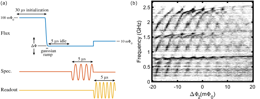
Following the spectroscopy pulse, for scans near plaquette 1 or 2 single frustration, the flux bias is then brought with a square pulse to a common readout point 10 m to the right of frustration. For scans near plaquette 3 single frustration, we read out at the same flux point as the spectroscopy because we need to overlap the spectroscopy pulse with the readout pulse in this case. This is likely due to a shorter lifetime for the plasmon states for plaquette 3 compared to that for plaquettes 1 and 2. For all the spectroscopy scans, we plot the quadrature distance between the heterodyne measurement of transmission through the feedline at the cavity resonance for the readout flux bias with and without a 5-s spectroscopy pulse.
Figure S6(b) shows an example of a spectroscopy measurement at single frustration for plaquette 2. The features that disperse gradually with flux correspond to the plasmon excitations within the well where the qubit is initialized, as described in Fig. 3 in the main paper; in addition to the 0-1, 0-2, and 0-3 transitions, we also observe transitions out of excited plasmon levels, indicating that the device is not fully initialized into the ground state of the well. In addition, we observe heavy fluxon transitions that disperse linearly with flux, and with a much steeper slope than the plasmons, that arise from transitions between levels in the and 0 wells. We observe qualitatively similar behavior for single frustration of plaquettes 1 and 3, as can be seen in the spectroscopy plots in Fig. S15.
For spectroscopy measurements at double and triple frustration, we add an extra step to stabilize the offset charge on the intermediate island(s) between the frustrated plaquettes. Details on this procedure are described in the next section.
VIII. Offset charge scans
As described in the main paper, Aharonov-Casher interference of the CW and CCW tunneling paths at various degrees of frustration results in a periodic modulation of the energy-level structure with respect to the offset charge on the island and the two intermediate islands between pairs of plaquettes. The modulation with offset charge on the island is difficult to observe directly in spectroscopy because the tunnel splittings for the low-lying levels are small. However, levels near the top of the barrier, which are also close to the readout cavity, exhibit a large modulation that leads to a significant periodic charge tuning of the readout cavity dispersive shift. The large physical footprint of the island results in a large effective charge sensing area, so that offset charge jumps occur on a timescale of a few minutes, as presented in Fig. 4(e) of the main paper.
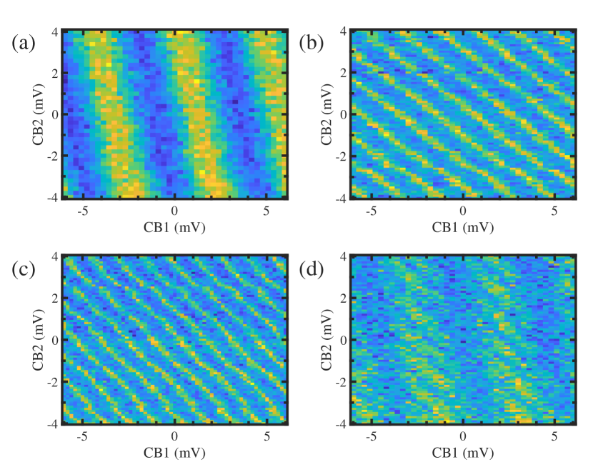
For measuring the modulation with respect to offset charge on the intermediate islands between plaquettes, we perform the spectroscopy sequence at the various combinations of double and triple frustration while applying a spectroscopy pulse at the 0-1 transition frequency for each particular frustration point and scanning the two island charge biases [Fig. S7]. Each of these two charge lines, CB1 and CB2, couples to the intermediate island adjacent to it, but there is also non-negligible crosstalk to the other intermediate island. Thus, in general, we observe a periodic modulation due to the charge sensitivity of the relevant for the particular frustration point, and these modulation features have a slope in the two-dimensional charge-bias space that depends on the capacitance between each bias line and the intermediate island(s) between the particular pair(s) of frustrated plaquettes. At plaquette (12) double frustration, the modulation is significantly faster with respect to CB1 because the capacitive crosstalk between CB2 and the intermediate island between plaquettes 1 and 2 is relatively weak [Fig. S7(a)]. By contrast, at plaquette (23) double frustration, the modulation is faster with respect to both CB1 and CB2 since the junction-chain inductors of plaquette 2 contribute to the intermediate island capacitance between plaquettes 2 and 3 and enhance its capacitance to both charge-bias lines [Fig. S7(b)]. The modulation is even faster for plaquette (13) double frustration, since now the effective intermediate island includes all of plaquette 2, which is unfrustrated, thus enhancing the capacitance to both charge-bias lines [Fig. S7(c)]. At triple frustration, we observe a double charge modulation, with one set of nearly vertical features corresponding to the modulation with respect to the offset charge on the intermediate island between plaquettes 1 and 2, and faster, more diagonal features from the modulation with respect to the offset charge on the intermediate island between plaquettes 2 and 3 [Fig. S7(d)]. From the slope and period of these various modulation features, we can extract the capacitance matrix between the charge bias lines and the plaquette islands (Table 2). These capacitances agree reasonably well with the Q3D numerical simulations of our device geometry [9].
| Simulated capacitance matrix (aF) | |||
|---|---|---|---|
| CB1 | CB2 | ||
| 57 | 419 | 353 | |
| Isl1 | 0 | 45 | 12 |
| Isl2 | 0 | 27 | 88 |
| Extracted capacitance matrix (aF) | |||
| CB1 | CB2 | ||
| 57 | 501 | 327 | |
| Isl1 | 0 | 35 | 8 |
| Isl2 | 0 | 73 | 120 |
While the offset charge jumps on the island occur every few minutes, we expect the offset charge jumps on the intermediate islands between plaquettes to be less frequent because of the much smaller charge sensing areas [10, 11]. In order to monitor offset charge jumps on both intermediate islands nearly simultaneously, we first scan the offset charge bias to island 1 (between plaquettes 1 and 2) at plaquettes (12) double frustratation while plaquette 3 is biased 50 m away from frustration; we then shift the fluxes slightly and scan the offset charge bias to island 2 (between plaquettes 2 and 3) at plaquette (23) double frustration while plaquette 1 is biased 50 m from frustration. We alternate back and forth between these two scans repeatedly over 11 hours (Fig. S8). As expected, given the smaller charge sensing areas, the offset charge on the intermediate islands jumps less frequently than on the island. The island between plaquettes 1 and 2, which has the smallest charge sensing area, is the most stable, with roughly 1 hour between large offset charge jumps.
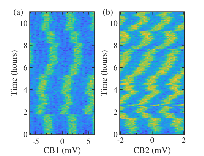
Despite the relative stability of the offset charge on the intermediate islands, we still need to actively stabilize the charge for long spectroscopy scans vs. flux at double and triple frustration, such as Fig. 4(b,c) in the main paper, to correct for occasional offset charge jumps. Thus, approximately every twenty minutes we interrupt the spectroscopy sequence to run a one-dimensional scan of the relevant intermediate island offset charge bias(es) while applying a spectroscopy pulse at the corresponding 0-1 transition frequency; each scan takes about 30 seconds. We then fit the resulting modulation signal with a cosine function to determine the appropriate adjustment to the charge bias to apply to maintain a constant total intermediate island offset charge.
In addition to the random offset charge jumps due to charge dynamics in the qubit environment, for example, from the impact of high energy particles [11], the various islands of our device are also subject to quasiparticle (QP) poisoning when a QP tunnels on or off the island. Because of the large physical footprint for the island, there will be spurious antenna resonances, as described in Refs. [12, 13], at frequencies extending from above the Al superconducting gap to below 100 GHz that couple resonantly to stray photons in the device environment and generate QPs at the plaquette junctions. In Fig. S9, we show measurements of spectroscopy near the 0-3 transition as a function of frequency and intermediate island offset charge near plaquette (12) and (23) double frustration. In both cases, we observe a periodic charge modulation of the transition, but with two bands that are offset by , indicating QP poisoning on the intermediate island between the plaquettes on a timescale faster than the spectroscopy measurement. Such QP poisoning will need to be significantly suppressed in future devices for the successful implementation of a protected qubit.
IX. Modeling of energy levels
Modeling multi-plaquette devices is challenging – our 3-plaquette chip with a SQUID switch has eleven phase degrees of freedom, and the size of the truncated Hilbert space is . Instead of choosing generalized coordinates manually, we use the SuperQuantPackage [14] to model the energy level spectra of the devices.
The SuperQuantPackage software framework was developed by Andrey Klots with the supervision of Lev Ioffe. This package is capable of modeling the energy spectrum of superconducting circuits with arbitrary configurations of Josephson junctions, capacitors, and inductors. The original flux coordinates of the nodes undergo a linear transformation that splits them into two classes: oscillator-like coordinates for which we choose a harmonic oscillator basis, and charge coordinates that correspond to clusters of nodes with quantized net charge and for which a natural charge basis is used. This automatically diagonalizes the inductive and capacitive parts of the Hamiltonian. At the same time, Josephson terms of the Hamiltonian assume a relatively simple and sparse form. Automatic assignment of physically meaningful coordinates does not require labor-intensive manual symmetry analysis of each configuration of all studied complex circuits. Meanwhile, it allows for efficient diagonalization of the Hamiltonians and relatively quick numerical convergence.
Despite this optimization of the numerics, modeling the full circuit of our most complex devices [Fig. S10(a)] would require at least several months on the most powerful processors available to our research group. Thus, we must devise strategies for simplifying the modeled circuit to make the calculation practical. A plaquette or SQUID biased at unfrustration behaves like a superconducting inductive short with an effective shunt capacitance. For example, when modeling single frustration, we simplify the circuit to a single plaquette connected in series with a resonator that represents the other unfrustrated plaquettes and SQUID-switch elements [Fig. S10(b)]. The resonator inductance and capacitance are shown in Fig. S10(b) as and . As shown in Fig. S10, each plaquette contains two arms, each having one Josephson junction in series with a linear inductor. The Josephson junction is characterized by and , where is the average energy of the Josephson junctions and is the charging energy set by the junction capacitance. The linear inductor is characterized by and , where is the average inductive energy of the junction-chain inductor and is the charging energy across the junction-chain inductor. From our fabrication uniformity tests, our nominally identical junctions exhibit a spread in of a few percent. We account for this asymmetry between the two junctions in a plaquette with the parameter , with and the Josephson energy of the left and right junction, respectively. Each arm has capacitance to ground, and this is characterized by . is the capacitance of the shunt. We introduce the parameter to account for variations in due to small flux offsets in the bias of the nominally unfrustrated plaquettes or SQUIDs. After this, we can input the circuit elements in the SuperQuantPackage.
The matrix is typically quite sparse, thus we can use the scipy.sparse.linalg.eigsh() function to find the eigenvalues and eigenvectors efficiently. This function only requires calculating the first few lowest eigenvalues, so the calculation speeds up. Typically, we only require the first 16-32 eigenvalues, but when we need to calculate the transitions involving the readout cavity, we need to calculate the first 40 eigenvalues.
The next step is finding the minimum number of states for each coordinate. We start by using three states for each cyclic coordinate and one state for each oscillator coordinate. We then vary the number of states from 1-20 for each coordinate, while tracking how the transition frequencies change. When the transition frequencies change by less than 5%, we choose the corresponding number of states for that particular coordinate for the next iteration. Using the new number of states, we repeat the same procedure until the process converges. In Fig. S11, we show the convergence for each of the coordinates as a function of the number of states for double frustration.
We model single frustration by considering a single plaquette connected in series with an circuit [Fig. S10(b)]. For double frustration, we model the unfrustrated elements as a single circuit in series with the two plaquettes that are modeled near double frustration [Fig. S10(c)].
A. Double plaquette flux dispersion vs. intermediate island capacitance
We modeled double frustration flux dispersion with different intermediate island capacitance, and we present some of these results in Fig. S12. When fF, the wavefunction is hybridized strongly between the and wells, resulting in a large and rather flat ground-state energy band [Fig. S12(a)]. The ground state energy band is relatively flat near frustration. When 5 fF, the effective mass along this direction is larger, but there is still somewhat effective hybridization between the and well [Fig. S12(b)]. In this case, , and the energy band curvature is larger. When 10 fF, the hybridization is significantly weaker [Fig. S12(c)]. and the antisymmetric level is now lower than the first excited plasmon state. Also, the energy bands have a nearly linear dispersion near double frustration. When 50 fF, the effective mass is so large that all four wells are nearly independent with vanishing coupling between them [Fig. S12(d)]; and the flux dispersion near double frustration is essentially linear.
B. Double plaquette flux dispersion for different
As shown in Fig. S14, when , the even-parity energy level and odd-parity energy level experience the same potential, and the energy levels are nearly degenerate, with the minimum separation at exact frustration. When the barrier heights between the , , , and wells become different. This leads to the even-parity energy levels and odd-parity energy levels experiencing different potentials, which causes the levels to cross on either side of frustration. The crossing points move further apart for larger .
C. Double plaquette charge dispersion at double frustration
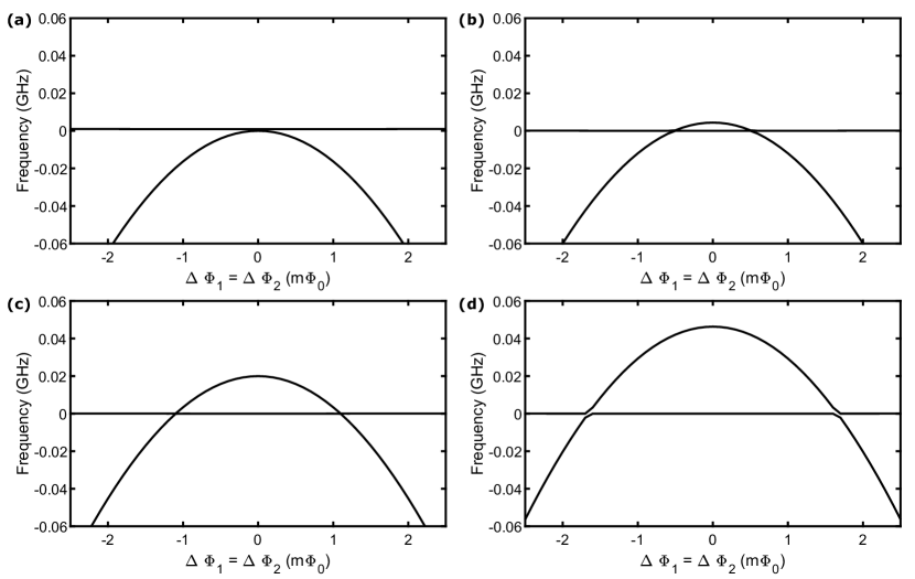
With effective hybridization at double frustration, the splitting between symmetric and antisymmetric levels exhibits Aharonov-Casher interference, based on the offset charge bias of the intermediate island between the frustrated plaquettes (Fig. S13). When , the symmetric/antisymmetric energy levels for both even and odd parity have periodicity. When the symmetric and antisymmetric energy levels cross at mod, the gap closes [Fig. S13(b)], because the even- (odd-) parity wavefunctions both experience a potential. When of plaquette 1 is 0.01 and of plaquette 2 is 0.03 [Fig. S13(c)], both of the gaps for even- and odd-parity states are not fully closed at mod due to incomplete destructive interference. When we bias the island charge at mod, the transition between the even- and odd-parity logical states is first-order insensitive to charge noise on the intermediate island.
D. Structureless plaquette model
Modeling a fully-structured three-plaquette circuit is computationally expensive, with 11 nodes [Fig. S10(d)], and each node requires several charge states. The matrix size is 189,000189,000, and thus requires 300 GB of RAM and takes weeks to calculate the energy levels, even with processors with 40 cores. As an alternative, we can use the stuctureless plaquette model to approximate the full-structure plaquette model.
We first connect one arm of the plaquette to form a loop, then vary the flux in this loop to obtain the potential of this arm. We next extract the Fourier components of this potential. In the structureless plaquette model, we replace the Josephson potential with the potential extracted from one arm of the plaquette. Thus, we do not need the linear inductors in the circuit, which reduces the number of effective nodes from 11 to 5, and the matrix size is now 7,0007,000. We add a renormalization factor in the junction capacitance to simulate the effect of higher internal levels. The need for this renormalization stems from the fact that the gap separating the potential energy of a single plaquette from the plaquette’s higher internal states is created by a massive Dirac-like Hamiltonian, which makes the flux particle effectively chiral. This chirality impedes tunneling, but cannot be implicitly accounted for in the structureless model. We mimic that by replacing this chiral property of a flux particle by increasing its effective mass by a renormalization factor that is fitted numerically by comparing structureless and full-structure plaquettes. For high internal excited state, the phase particle is less chiral and the renormalization factor is and low-lying internal excited states make the flux particle more chiral and yield a renormalization factor from to in the most unfavorable cases. We find the structureless plaquette model has a good agreement with the full-structure plaquette near frustration. We thus use the strucureless plaquette model for the remainder of this section.
E. Triple-frustration modeling
We model the triple-frustration flux dispersion for a simultaneous scan of the flux bias to each plaquette along a line from 000 to in Fig. S21. In Fig. S21(a), at tripled frustration, the computational states are a superposition of even-parity wells (, , , ) and a superposition of odd-parity wells (, , , ). In the ideal case of symmetric plaquettes and small flux offsets, the nearly-degenerate computational states are that correspond to even and odd charge parities. However, as we go away from the protected regime, the computational states turn into even () and odd () flux states. A few away from triple frustration, the lowest energy level corresponds to the wavefunction localized only in the 000 or well. The second lowest levels correspond to a superposition of , , on the left and , , on the right. The energy levels for the 0 and 1 logical states both have negative curvature with respect to flux, so the flux dispersion of the 0-1 transition is flatter compared to double frustration, thus further enhancing the protection against flux noise.
X. Fitting of energy-level spectra
A. General fitting strategy
For extracting the center frequency of each transition at every flux point, the complexity of the level spectrum for our device makes it not practical to implement an automated routine that fits a standard curve to each feature in the spectroscopy data. Instead, we identify each transition feature in the data manually, then extract the maximum of the spectroscopy signal for each of these features. We then check the correspondence of the extracted transitions with our numerical model of the energy-level spectrum. We use the initial estimates for the various device parameters to calculate the energy levels, which generally match the data qualitatively. From this, we can identify most of the transitions. During the first round of fitting, where we adjust the circuit parameters about their estimated values to match with the transition data, described in detail below, we only fit the transitions that we have identified correctly in the initial step. Following this stage, the fitted energy levels typically match with the data quite well and we can identify more transitions. We then use the newly identified transitions to further refine the fit.
After extracting the plasmon, heavy fluxon, and light fluxon transitions, as well as the anticrossings from the spectroscopy flux- and charge-dependence data, we use the single (double) plaquette model for the energy-level spectra described in Sec. IX. to fit the single- (double-) frustration spectroscopy data. At single frustration, we fit , , , , , , and using the model shown in Fig. S10(b). We fix to be 1 fF, which is estimated from numerical modeling with Q3D and a theoretical estimation of the effect of the junction chain capacitance to ground. We introduce the parameter to account for variations in due to small flux offsets in the bias of the nominally unfrustrated plaquettes or SQUIDs. At double frustration, we fit the same parameter set as in the single frustration case, but with the addition of . Similarly to the single frustration case, we fix to be 1 fF. We assume the two plaquettes at frustration share the same set of parameters, because the actual parameters between the two plaquettes are typically only different by a few percent based on our test structures during the device fabrication. This allows us to reduce the number of fitting parameters from 15 to 8, and thus makes the fitting more practical.
The cost function of our fitting procedure is , where is the difference between the modeled and experimental frequencies for transition , and is the weight that we assign to transition . The goal of the fitting process is to minimize the cost function and find the parameter set that has less than a 10% difference between the modeled transitions and the experimental transitions. We use the scipy.optimize.minimize function in Python to do the fitting. We have 7 and 8 parameters for single- and double-frustration fitting, respectively. We find that the Nelder-Mead method performs better for this fitting than gradient descent methods in terms of avoiding local minima.
With this high-dimensional fit, we need to choose the initial parameters carefully. We use the initial and values calculated from the Ambegaokar-Baratoff relation using the on-chip test junction resistances. The initial of the junctions is estimated from our test chips that each contain 6 identical junctions. As mentioned earlier, we define the charging energy as . The initial and values are calculated from the the relevant junction areas measured with scanning electron microscopy with a total specific capacitance 70 fF/m2. The initial is estimated from Q3D simulation. The initial is set to 1 because our unfrustrated plaquettes are nominally biased at unfrustration. We choose the initial simplex for the minimization so that it covers the possible range for each parameter, which is typically to of the initial values.
B. Single frustration fitting
We fit the single frustration data with our single plaquette model [Fig. S10(b)]. We put equal weight on different transitions by setting for the fitting. The fit runs on a computer with a 12-core processor and takes 1 day and 500 iterations to converge. In Fig. S15(c), we show the fitting of plaquette 2 single frustration. The red lines correspond to the fitted plasmon transitions, and the blue lines correspond to the fitted heavy fluxon transitions. The dotted lines are transitions out of the state, corresponding to the 0 level of the well. The dash-dotted lines are transitions out of the state. The dashed lines are transitions out of the state. The transitions match with the data within 10% error. In Fig. S15(a), we show the modeled energy levels using the fitting parameters and indicate some example plasmon and fluxon transitions out of the , and states.
In Fig. S15(b-d), we show the single frustration fitting of plaquette 1, 2, 3 single frustration. Plaquette 1 behaves similarly to plaquette 2, and thus the fitted transitions and parameter values are similar. Plaquette 3 single frustration behaves somewhat differently, and the fitted energy levels and parameters differ by a larger amount compared to plaquettes 1 and 2. The fitted parameters are listed in Table 3 and they are within 20% of the parameters that we estimate from the design and fabrication tests, although a few of the parameters for plaquette 3 have a slightly larger discrepancy. The spectroscopy measurements at plaquette 3 single frustration are not as clean as for plaquettes 1 and 2 single frustration, thus potentially accounting for the larger variation with the estimated values.
|
|
|
|
|
|||||||||||||
|---|---|---|---|---|---|---|---|---|---|---|---|---|---|---|---|---|---|
| Plaquette 1 | 1.65 | 3.65 | 1.12 | 5.60 | 1160 | 0.03 | 1.1 | ||||||||||
| Plaquette 2 | 1.65 | 3.67 | 1.11 | 6.36 | 1190 | 0.02 | 1.1 | ||||||||||
| Plaquette 3 | 1.97 | 4.00 | 1.27 | 6.66 | 1440 | 0.04 | 0.91 | ||||||||||
|
1.45 | 3.82 | 1.39 | 6.46 | 1000 | 0.02 | 1.0 |
C. Double frustration fitting
We next use the model in Fig. S10(c) to fit the double frustration data. Because the Hilbert space is 11 times larger at double frustration using this model, we use a 48-core processor to do the fitting. This process takes between 4-7 days and 300 iterations to converge. The anticrossings between different transitions are important features to fit because they determine the coupling between the computational states, so we put 20 times more weight for the regions in the spectroscopy data that exhibit significant anticrossings. We also simultaneously fit the corresponding charge modulation data and we only use the minimum and maximum of the charge modulation data for fitting. In order to compensate for the relatively small number of charge modulation data points, we put 50 times more weight for these features in the fitting.
In Fig. S16(b), we show the plaquette (12) double frustration data and fitted transitions. The red lines are the fitted plasmon transitions, the blue lines are the fitted heavy fluxon transitions, and the purple lines are the fitted light fluxon transitions. The dotted lines are transitions out of the state, where corresponds to the even-parity hybridized well between plaquettes 1 and 2, corresponds to the symmetric hybridized energy level of plaquettes 1 and 2, and 0 corresponds to the lowest energy level with these conditions. The dash-dotted lines are transitions out of the state and the dashed lines are transitions out of the state. The red solid line is , which is the transition out of the 0 state of the antisymmetric energy levels in the even-parity wells to the 1 state of the antisymmetric energy levels in the even-parity wells. We see this transition because there is fast quasiparticle poisoning on the intermediate islands that is faster than our measurement timescale. When we prepare the qubit in the state, the fast quasiparticle poisoning closes and opens the symmetric and antisymmetric gap randomly, which allows the system to occasionally transfer population from the to states, thus leaving population in the excited antisymmetric state. This results in the transition indicated by the solid red line in Fig. S16(b). In Fig. S9(b), we show the plaquette (12) double frustration charge modulation data of the transition at 17 m. We can clearly see two quasiparticle bands, which we indicate by the red and blue dotted lines for the fitted transitions. We show the flux dependence of the fitted energy levels and corresponding transitions in Fig. S16(a). In Fig. S9(c), we show the plaquette (23) double frustration charge modulation data of the transition at 11 m.
In Fig. S16(b-d), we show the fit results for the flux spectroscopy at plaquette (12), (23), and (13) double frustration. The for (12), (23), and (13) double frustration are 2.7, 1.0, and 0.5 GHz, respectively, as expected for a decreasing and progressively weaker hybridization for a larger intermediate island capacitance to ground. The fitted curves capture the transitions, anticrossings, and charge modulation to within 10%. The fitted parameters are shown in Table 4 and are in reasonable agreement with our estimated parameters.
In Fig. S16(c,d), the solid black lines between -20 to -10 m in the plaquette (23) and (13) double frustration plots correspond to transitions involving the readout cavity: , where and indicate photon number in the cavity.
Near double frustration, as described in the schematic plots in Fig. 1(k) in the main paper, the parity of the initial state and the direction of the scan through the 2D flux-bias space determines which levels will disperse with respect to flux and which will be flat. For example, preparation in an even-parity state, say, , followed by a scan in the even-parity flux-bias direction, so, going from a flux bias where the well is the global minimum to a flux where the 00 well is the global minimum, should result in the even-parity levels dispersing with flux while the odd-parity levels should be flat. This behavior should swap for the opposite parity of the initialized state and scan direction.
To examine this difference, we measure single-frequency spectroscopy scans in the 2D flux-bias space near plaquette (12) double frustration for both even- and odd-parity initializations [Fig. S17]. For each point in Fig. S17(a), we initialize in the well near double frustration, then bring the flux bias to the point indicated in the 2D flux space, apply a spectroscopy pulse at 720 MHz, and then bring the flux bias to double frustration to read out [Fig. S17(a)]. The axes of the plot correspond to the even- and odd-parity flux directions. The black dots along the 00 to direction indicate the points where we see transitions cross 720 MHz in our simulation of the spectrum [Fig S17(b)]. These points correspond to the transitions that are visible in the spectroscopy scan in Fig. 4(b) of the main paper. To identify the somewhat hyperbolic features away from the even-parity flux-bias axis in the odd-parity flux-bias direction, we consider the modeled level spectrum for a preparation in the even-parity well, with a scan along the odd-parity flux-bias direction [Fig S17(c)]. For flux-bias points of 10 m or more away from frustration, there are many transitions out of the flat even-parity level up to the dispersing odd-parity levels. The transitions that match the 720 MHz spectroscopy frequency are labeled by red dots. If the odd-parity flux-bias scan is done for a nonzero offset along the even-parity flux-bias axis, the points that correspond to this same spectroscopy frequency shift in position, as shown again by the red dots.
If we now initialize in an odd-parity well, the well in this case, then repeat the same measurement process [Fig. S17(d)], we see that all of the features from the scan with even-parity initialization repeat, but are now rotated by 90 degrees. We again perform the same numerical modeling process for the level structure, but now with the initial state and the parity of the simulated flux-bias axes swapped [Fig. S17(e,f)]. Again, the features visible in this 2D spectroscopy scan match up with the various transitions that we identify in the modeled level spectrum.
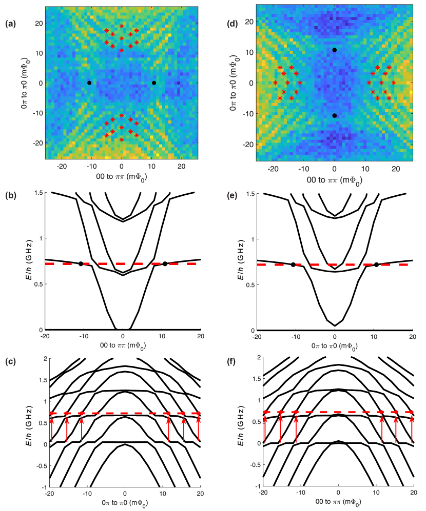
|
|
|
|
|
|
|||||||||||||||
|---|---|---|---|---|---|---|---|---|---|---|---|---|---|---|---|---|---|---|---|---|
|
1.75 | 3.54 | 1.20 | 6.34 | 1240 | 0.03 | 1.5 | 0.99 | ||||||||||||
|
1.76 | 3.53 | 0.900 | 7.40 | 1290 | 0.04 | 5.7 | 1.0 | ||||||||||||
|
1.73 | 3.48 | 0.903 | 6.62 | 1310 | 0.03 | 8.1 | 0.98 | ||||||||||||
|
1.45 | 3.82 | 1.39 | 6.46 | 1000 | 0.02 | Vary* | 1.0 |

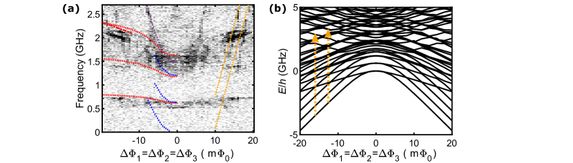
D. Triple frustration modeling
We model the triple frustration data with the circuit in Fig. S10(d). The Hilbert space of this triple frustration model is 100 times larger than for the double frustration model. Modeling one flux point takes 10 days, so it is impossible to model several flux points and fit to the triple frustration data. We model the triple frustration energy levels by simultaneously modeling different flux points on four virtual machines in parallel, which have 48-, 24-, 12- and 12-core processors, respectively. In each of the virtual machines, we use the multiprocess function in Python to model different flux points in parallel so that it uses all the computational power in that virtual machine. Because fitting is not practical here, we use the fitted parameters from the single- and double-frustration modeling, and only adjust the to account for the SQUIDs not being at exact unfrustration. Figure 4(c) in the main paper shows the triple frustration flux spectroscopy data and modeled transitions. The red lines are the modeled plasmon transitions, the blue line is the modeled heavy fluxon transition, and the purple line is the modeled light fluxon transition. The dotted lines are transitions out of the 0 state of the symmetric energy levels in the even-parity wells. Based on our modeling, we find the plasmon and light fluxon transitions are in good agreement between our modeled curves and the triple frustration data. In general, we observe that the transitions at triple frustration have an even flatter dispersion with respect to flux compared to double frustration. As shown in Fig. S18, within m of triple frustration, the heavy fluxon transitions and plasmon transitions are difficult to distinguish, as the even-parity and odd-parity energy levels are likewise nearly on top of each other. Because of this, the dispersion of the various heavy fluxon transitions, , is comparable and rather flat.
Figure S19 shows the light fluxon transition plus cavity photon, which is visible near the edges of our triple frustration spectroscopy data, and the comparison with the modeled level spectrum. The difference between the levels indicated by arrows minus the readout cavity frequency matches these particular features in our data.
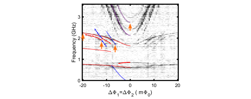
| Parameter uncertainty estimates within a 10% range based on: | |||||||||||||||||||||||||||||||||||
|
|
|
|
|
|
|
|||||||||||||||||||||||||||||
| (a) Plasmon transition ( transition at 20 m) | |||||||||||||||||||||||||||||||||||
|
|
|
|
|
|
|
|
|
|||||||||||||||||||||||||||
| (b) Heavy fluxon transition ( transition at 6.5 m) | |||||||||||||||||||||||||||||||||||
|
|
|
|
|
|
|
|
|
|||||||||||||||||||||||||||
| (c) Light fluxon transition ( transition at 0 m) | |||||||||||||||||||||||||||||||||||
|
|
|
|
|
|
|
|
|
|||||||||||||||||||||||||||
|
|||||||||||||||||||||||||||||||||||
|
|
|
|
|
|
|
|
|
|||||||||||||||||||||||||||
| (e) Intersection of fitted errors estimated from four types of transitions | |||||||||||||||||||||||||||||||||||
|
|
|
|
|
|
|
|
|
|||||||||||||||||||||||||||
E. Fit parameter error estimation
In general, each type of transition has a different sensitivity to the various fitting parameters for the device. In order to estimate the uncertainty in each fitted parameter, we compute the energy level spectrum while varying each parameter one at a time and keeping the other parameters at their best-fit values. We thus find the range over which each parameter can be varied while keeping the transition frequencies within 10% of the measured values. In Fig. S20, we show the four transitions we choose to estimate the fitted errors. In Table 5(a), we list the fitted errors obtained with this method for the plasmon transition at 20 m. From this table, we see the plasmon transition is sensitive to , , , and , so we are confident of the parameters extracted from fitting the plasmon transitions. In Table 5(b), we list the fitted errors for the heavy fluxon transition at 6.5 m. The heavy fluxon transition is especially sensitive to , , while moderately sensitive to the rest of the parameters, so by fitting to the heavy fluxon transition, we have high confidence in the , values, with moderate confidence in the rest of the parameters. In Table 5(c), we list the fitted errors for the light fluxon transition at 0 m. The light fluxon transition is quite sensitive to , , , , and , so these fitted parameters extracted from fitting the light fluxon transition have small errors. In Table 5(d), we list the fitted errors for the anticrossing between the transition and the transition at 12 m. The anticrossing is highly sensitive to , , , so the errors for these fitted parameters by fitting the anticrossing are quite small. Our fitting method fits all four types of transitions, so we are confident that the parameters of the actual chip are within the intersection of the estimated errors extracted from these four types of transitions, as shown in Table 5(e).
XI. Prospects for implementing protected qubits
Our experiment presented in the main paper demonstrates successful concatenation of -periodic plaquettes through measurements of large and offset-charge tuning, characteristic of strong hybridization of frustrated plaquettes. In order to implement a protected qubit based on this approach, we need a device that robustly maintains nearly degenerate computational states while pushing the remaining fluxon and plasmon energy levels significantly upwards. This means that for qubit design, we want to gain control over the three major energy scales: (1) Heavy fluxon gap , that is also the computational gap that protects from -processes and charge noise, needs to be kept small; (2) Light fluxon gap , that determines effectiveness of concatenation and protects from flux noise and -processes, needs to be kept large; (3) Plasmon gap that determines energies of unwanted low-lying plasmon states that deteriorate initialization fidelity and facilitate thermal excitations, needs to be kept high. For determining these energy scales, there are three primary device parameters that can be adjusted in the design: Shunt capacitance ; Effective intermediate island charging energy , that is determined by both the geometric ground capacitance of the intermediate island and the effective screened capacitances of the Josephson junctions that also indirectly couple the intermediate island to ground; of an individual plaquette, that is mainly determined by a combination of . The table below demonstrates how the three energy gaps change as the described device parameters increase. The entries of the table describe whether or not the gaps change in the desired direction, and whether they change exponentially (exp) or (sub)polynomially (poly). Each entry is also accompanied by a brief explanation.
| as increases | as increases | as increases | |
| GOOD; exp | BAD; weak poly | GOOD, exp | |
| lower is better | interwell tunneling as mass | of chain slightly decreases | interwell tunneling as barrier |
| because hybridization washes out | |||
| the top of potential | |||
| N/A | GOOD; poly | BAD; poly | |
| higher is better | no strong depenence as | lighter fluxons hybridize better | hybridization as barrier |
| ideally, light fluxon modes | |||
| are decoupled from | |||
| BAD, poly | BAD, weak poly | GOOD, poly | |
| higher is better | of chain slightly decreases |
Note that each of these device parameters improves some energy scales, while deteriorating others. Thus, the goal of optimization is not to just maximize some circuit parameters, but to compensate the negative effects by tuning other parameters. For example, increasing significantly improves concatenation (light fluxon modes), but negatively, albeit weakly, affects the heavy fluxon and plasmon modes. Therefore, it is always beneficial to increase , while keeping in mind the presence of mild adverse effects. On the other hand, increasing and is exponentially beneficial for the computational gap, but (sub)polynomially adversely affects concatenation (light fluxon) and the plasmon modes. It is encouraging that adverse effects of increasing and are smaller than the benefits. However, these adverse effects are not negligible and need to be treated very carefully. In addition to these device parameters that can be controlled through design, there are also uncontrolled ones, such as the flux noise amplitude and junction asymmetry . However, improved concatenation protects the device against these types of asymmetries. This means that decreasing would also increase polynomially – as a power of the number of plaquettes minus one.
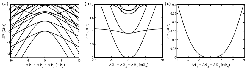
One set of parameters that provides a compromise between the competing circuit parameters needed for achieving a qubit with excellent coherence is the following: K, K, K, fF, fF, fF, . Unfortunately, achieving these values of and with conventional Al electrodes is not possible due to the small superconducting gap and the electronic capacitance arising when the junction plasma frequency approaches the gap [5]. Thus, protected qubits incorporating this stabilizer mechanism will need junctions fabricated from a larger gap superconductor. Reducing from 0.03 in our experimental device to 0.01 will be challenging, but should be achievable with improved control over the electron-beam lithography and thin-film growth for forming the junctions. Reducing the intermediate island capacitances from our experimental device in the main paper to the values listed above requires minimizing the size of the intermediate islands as well as the length of the junction chain inductors, but the levels listed here are feasible. An alternate approach for satisfying the competing constraints involving parallel chains of concatenated plaquettes will be discussed at the end of this section.
In addition to optimizing the device parameters as described above, the device layout must have weaker radiative coupling to parasitic high-frequency modes to avoid spurious excitations and fast quasiparticle poisoning of the intermediate islands. Achieving this in practice is challenging because of the large . On our present device, the planar capacitor layout for required an exceedingly large physical footprint, resulting in significant low-frequency parasitic modes that couple strongly to the qubit environment. For a future protected qubit implementation, switching to a parallel-plate capacitor for would allow for a much more compact structure, thus pushing parasitic antenna modes to much higher frequencies. For a conventional superconducting qubit, such as a transmon, the microwave losses for the deposited amorphous dielectric layer in such a capacitor would result in quite poor performance. However, for a qubit formed from concatenated -periodic plaquettes with a large , the transition matrix elements between the logical qubit states are quite small. When combined with the vanishingly small value for , this results is an extremely long , even with the large loss tangent for the deposited dielectric of , as will be discussed below in our treatment of the projected coherence times.
In order to estimate the coherence for a protected qubit based on this design with the parameters described earlier in this section, we first compute the level spectrum for such a device at triple frustration (Fig. S21). With these , , and values, the separation between the logical qubit states is quite flat with respect to flux, with a minimum separation () of kHz. The lowest plasmon transition is also pushed up to nearly 1 GHz above the ground-state doublet. At plaquette (12) and (23) double frustration, the symmetric-antisymmetric gaps are GHz and GHz, and so are comparable with the lowest plasmon transition.
Upon computing the level spectrum near triple frustration for this set of parameters, we can estimate the qubit coherence. For obtaining , we first calculate the transition matrix element for the charge operator between the even- and odd-parity ground states (, respectively) at triple frustration for the above parameters: . can then be expressed as
| (S2) |
Assuming we fabricate a parallel-plate shunt capacitor using electron-beam evaporated SiO2, which is compatible with our current device fabrication process, the corresponding loss tangent is 1/300 [15], resulting in s. In general, for our architecture, the budget is quite high because it is determined by exponentially weak and easily suppressable interwell tunneling. The much bigger challenge is creating flat bands to enhance .
For computing for the device described above, we consider the flux dispersion of the energy bands from our numerical modeling. Exactly at triple frustration, the slope with respect to flux bias vanishes and the curvature is MHz/. Assuming the electronics used for supplying the flux-bias currents is capable of sufficiently fine steps, the flux resolution of our biasing will ultimately be limited by the rms flux noise level . We calculate the -noise-limited with the formula:
| (S3) |
where the flux noise is assumed to follow the power spectrum , we consider a Ramsey pulse performed immediately after calibration. Taking a flux-noise power spectral density of at 1 Hz and integrating over 10 decades yields an rms flux noise level of 10 . Accounting for these various factors, we compute a flux-noise limited dephasing time for single frustration, plaquette (12) double frustration, plaquettte (23) double frustration, and triple frustration: s, s, s, s, respectively.
We also consider dephasing due to charge noise at triple frustration by computing the level of fluctuations in the splitting between the computational levels. We estimate the lower limit of with
| (S4) |
where we assume a charge noise power spectrum and we again, like in the case of flux noise, assume that the Ramsey pulse is performed immediately after calibration. For a charge-noise spectral density of at 1 Hz [16, 10], we estimate a charge-noise limited dephasing time, s. This timescale decreases for larger , for example, with a smaller . Thus, reducing in an attempt to increase , will eventually cause dephasing due to charge noise to become non-negligible as increases.
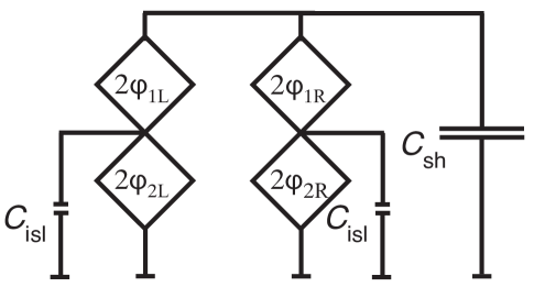
In addition to the optimization of our multi-plaquette chain discussed above, there are alternative device geometries that can mitigate the adverse effects of decreasing . For example, connecting multiple plaquette chains in parallel, as shown in Fig. S22, results in a linear increase in the overall system , thus raising the plasmon modes without the need for increasing of the individual plaquettes, which is helpful for maintaining strong concatenation. This allows for the use of a smaller for raising the plasmon transition frequencies without sacrificing an increase in . Of course, such an approach with two 3-plaquette chains will require twice as many flux bias controls compared to a single chain, plus one more flux bias for the loop formed by the two chains.
XII. calculation
As described in the main paper, characterizes the rate at which the logical error decreases with system size. can be expressed either as the ratio of between the larger and smaller system sizes, or, in the specific case of a qubit based on concatenated plaquettes, can also be determined by and , the scale of dephasing fluctuations for a single plaquette. In this section, we show that these two approaches are essentially equivalent. In addition, we compute for different degrees of frustration for a qubit with the optimal parameters described in the previous section. For a given level of flux noise, will be inversely proportional to the slope of the qubit transition energy with respect to flux. Thus, computing from the ratio of the values will be equivalent to the inverse ratio of the energy band slopes for the two different degrees of frustration.
For the semi-quantitative description of the system at double frustration presented in the main paper, we can treat each plaquette as a spin-1/2 particle with an stabilizer term. The energy of each plaquette is , where is the slope of the transition energy with respect to flux, and is the flux offset from frustration for plaquette . In this model, the double-plaquette Hamiltonian is then:
| (S5) |
Here, we assume the two plaquettes have the same . The eigenvalues are
| (S6) |
The double-plaquette circuit typically has MHz and GHz. Near single frustration for one of the plaquettes, the other plaquette will have near 0.5 , thus . In this limit, we obtain:
| (S7) |
Thus, the transition energy between the lowest two energy levels is and the corresponding slope is
| (S8) |
where S indicates single frustration.
Near double frustration, the slope is highest in the or directions. Taking , the energy levels are
| (S9) |
The transition energy between the lowest two energy levels is , and the corresponding slope with respect to is . For a flux noise level of 2 at 1 Hz, the rms flux noise amplitude is 10 , and we take this to be the minimum precision with which one can set the flux bias. For typical double-plaquette parameters, MHz and GHz. In this limit, , and the slope of the transition energy with respect to flux at double frustration is
| (S10) |
where D indicates double frustration. , the decrease in the logical error rate upon going from single to double frustration, is then
| (S11) |
Thus, in this approximation, defined as the ratio of at double and single frustration is equal to the ratio of to , where the factor of 2 accounts for the two plaquettes.
For triple frustration, the Hamiltonian for the coupled spin-1/2 model of a 3-plaquette chain is given by
| (S12) |
assuming all three plaquettes have the same single-frustration slope . Finding the eigenvalues of this Hamiltonian and expanding them to third order in the limit of and , we find the transition energy of the lowest two levels is . The corresponding slope with respect to flux is
| (S13) |
where indicates triple frustration.
We can then express , the reduction in logical error rate upon going from double to triple frustration by taking the ratio of the expressions in Eq. (S11) and Eq. (S13). Thus, for plaquette (12) double frustration, we obtain
| (S14) |
and for plaquette (23) double frustration, we obtain
| (S15) |
Then, , the reduction in logical error rate upon going from single to triple frustration, is given by
| (S16) |
|
|
|
|
|||||||||||||||||||
|
- | 380 | - | 1.7 | - | - | - | - | - | - | ||||||||||||
|
1.5 | 1.8 | 340 | 200 | 200 | 180 | 150 | - | - | |||||||||||||
|
0.87 | 3.2 | 190 | 110 | 120 | 320 | 270 | - | - | |||||||||||||
|
- | - | - | - | - |
In Table 6, we list the various energy scales and energy band parameters for the device with optimal parameters, described in Sec. XI., as well as the values calculated from the modeled energy levels. We also list the values for the various degrees of frustration, calculated both from the ratio of values from the modeled energy levels and from and . We see that both approaches for computing are in agreement, consistent with our analysis described above.
References
- Lefevre-Seguin et al. [1992] V. Lefevre-Seguin, E. Turlot, C. Urbina, D. Esteve, and M. H. Devoret, Physical Review B 46, 5507 (1992).
- Mooij et al. [1999] J. Mooij, T. Orlando, L. Levitov, L. Tian, C. H. Van der Wal, and S. Lloyd, Science 285, 1036 (1999).
- Manucharyan et al. [2009] V. E. Manucharyan, J. Koch, L. I. Glazman, and M. H. Devoret, Science 326, 113 (2009).
- Koch et al. [2007] J. Koch, M. Y. Terri, J. Gambetta, A. A. Houck, D. Schuster, J. Majer, A. Blais, M. H. Devoret, S. M. Girvin, and R. J. Schoelkopf, Physical Review A 76, 042319 (2007).
- Eckern et al. [1984] U. Eckern, G. Schön, and V. Ambegaokar, Physical Review B 30, 6419 (1984).
- [6] InductEx, SUN Magnetics.
- Foxen et al. [2018] B. Foxen, J. Mutus, E. Lucero, E. Jeffrey, D. Sank, R. Barends, K. Arya, B. Burkett, Y. Chen, Z. Chen, et al., Superconductor Science and Technology 32, 015012 (2018).
- Rol et al. [2020] M. A. Rol, L. Ciorciaro, F. K. Malinowski, B. M. Tarasinski, R. E. Sagastizabal, C. C. Bultink, Y. Salathe, N. Haandbæk, J. Sedivy, and L. DiCarlo, Applied Physics Letters 116, 054001 (2020).
- [9] ANSYS, ANSYS Q3D Extractor.
- Christensen et al. [2019] B. Christensen, C. Wilen, A. Opremcak, J. Nelson, F. Schlenker, C. Zimonick, L. Faoro, L. Ioffe, Y. Rosen, J. DuBois, et al., Physical Review B 100, 140503 (2019).
- Wilen et al. [2021] C. Wilen, S. Abdullah, N. Kurinsky, C. Stanford, L. Cardani, G. d’Imperio, C. Tomei, L. Faoro, L. Ioffe, C. Liu, et al., Nature 594, 369 (2021).
- Rafferty et al. [2021] O. Rafferty, S. Patel, C. Liu, S. Abdullah, C. Wilen, D. Harrison, and R. McDermott, arXiv preprint arXiv:2103.06803 (2021).
- Liu et al. [2022] C.-H. Liu, D. C. Harrison, S. Patel, C. D. Wilen, O. Rafferty, A. Shearrow, A. Ballard, V. Iaia, J. Ku, B. Plourde, et al., arXiv preprint arXiv:2203.06577 (2022).
- Klots [2022] A. R. Klots, SuperQuantPackageV2 (2022), [Online; accessed 6. Jul. 2022], URL https://github.com/andreyklots/SuperQuantPackageV2.
- O’Connell et al. [2008] A. D. O’Connell, M. Ansmann, R. C. Bialczak, M. Hofheinz, N. Katz, E. Lucero, C. McKenney, M. Neeley, H. Wang, E. M. Weig, et al., Appl. Phys. Lett. 92, 112903 (2008), ISSN 0003-6951.
- Astafiev et al. [2006] O. Astafiev, Y. A. Pashkin, Y. Nakamura, T. Yamamoto, and J.-S. Tsai, Physical Review Letters 96, 137001 (2006).