Impact of edge morphology and chemistry on nanoribbons’ gapwidth
Abstract
In this work, we scrutinise theoretically how the gap of C and BN armchair nanoribbons changes upon variations of the bond length between edge atoms and their distance from passivating species. Our DFT calculations indicate that the gap of C-based nanoribbons is more sensitive to the relaxation of the bonding length between edge atoms (morphology) whereas in BN-nanorribons it is more sensitive to the distance between edge atoms and passivating hydrogens (chemical environment). To understand the origin of these two different behaviours, we solved a tight-binding ladder model numerically and at the first-order perturbation theory, demonstrating that the different dependence is due to the interference of the wavefunctions of the top valence and the bottom conduction states.
I Introduction
In recent decades, graphene and hexagonal boron nitride (BN) have attracted a great deal of interest because of their remarkable transport and optical properties Geim and Novoselov (2007); Watanabe et al. (2009); Castro Neto et al. (2009); Weng et al. (2016); Zhang et al. (2017). A much explored way to modulate them is by adding extra confinement (as in 2D quantum dots, nanoribbons or nanotubes). The presence of confining edges endows them with novel size-dependent features dominated by the characteristics of the edge itself. This is why graphene and BN nanoribbons are often classified according to their edge shape, which can be zig-zag, armchair, fall in an intermediate chiral angle, or present structures that require a more general nomenclature Ezawa (2006). In zig-zag nanoribbons, well localised edge-state are formed which confer antiferromagnetic properties to C-based zig-zag nanoribbons Ezawa (2006); Fujita et al. (1996); Nakada et al. (1996); Behzad and Chegel (2018); Wakabayashi et al. (1999); Yang et al. (2007); Son et al. (2006). Instead, BN-based zig-zag nanoribbons have an indirect gap and display an intrinsic dipole moment Behzad and Chegel (2018); Nakamura et al. (2005); Park and Louie (2008); Wang et al. (2011); Shyu (2014); Topsakal et al. (2009); Zhang and Guo (2008); Ding et al. (2009). At variance, both graphene Ezawa (2006); Nakada et al. (1996); Behzad and Chegel (2018); Wakabayashi et al. (1999); Yang et al. (2007); Son et al. (2006); Nematian et al. (2012); Barone et al. (2006); Jha et al. (2019); Nishad et al. (2020); Prabhakar and Melnik (2019); Ren et al. (2007); Lu et al. (2009); Raza and Kan (2008) and BN Behzad and Chegel (2018); Park and Louie (2008); Wang et al. (2011); Shyu (2014); Zhang and Guo (2008); Topsakal et al. (2009) armchair nanoribbons (AGNR and ABNNR), have no magnetic states and display a direct size-dependent gapwidth To take full advantage of this richness of properties, several methods have been explored including the application of external electromagnetic fields Behzad and Chegel (2018); Wakabayashi et al. (1999); Park and Louie (2008); Zhang and Guo (2008); Raza and Kan (2008), strain Topsakal et al. (2009); Prabhakar and Melnik (2019); Li et al. (2010) and edge engineering Topsakal et al. (2009); Barone et al. (2006); Ding et al. (2009); Jha et al. (2019); Nishad et al. (2020); Lu et al. (2009); Prabhakar and Melnik (2019); Zheng et al. (2013); Ren et al. (2007).
As a matter of fact, the edge characteristics are crucial for the performances of nanoribbon-based devices such as transistors, interconnects and logical devicesMurali et al. (2009); Zheng et al. (2013); Das et al. (2021); Marmolejo-Tejada and Velasco-Medina (2016); Nishad et al. (2020); Saraswat et al. (2021), photovoltaic applications Osella et al. (2012); Saraswat et al. (2021), or chemical sensingMehdi Pour et al. (2017); Saraswat et al. (2021). Experimentally, edge engineeringSchwab et al. (2015); Wang et al. (2016); Osella et al. (2012), chemical treatmentDauber et al. (2014) or selective passivationZheng et al. (2013) have been demonstrated to have a significant impact on the device quality, precisely because of their action on the edges.
Alterations of the electronic structure due to edge modifications can be divided into morphology effects (variation of the bondlengths) and chemistry effects (variation of the passivating species and their distance from the edges)Ezawa (2006); Lu et al. (2009). The sensitivity of AGNR and ABNNR gap to the passivation has been investigated by many authors Ezawa (2006); Barone et al. (2006); Ding et al. (2009); Jha et al. (2019); Nishad et al. (2020); Topsakal et al. (2009); Lu et al. (2009); Prabhakar and Melnik (2019); Zheng et al. (2013); Ren et al. (2007) who showed that its effect depends on the type of atoms involved, and/or on the number and position of the passivated sites. Most of these first-principle studies Barone et al. (2006); Ding et al. (2009); Jha et al. (2019); Nishad et al. (2020); Topsakal et al. (2009); Prabhakar and Melnik (2019); Ren et al. (2007) discuss the role of passivation on fully relaxed structures, so morphology and chemistry effects are actually treated on the same footing. At best of our knowledge, only two studies Ezawa (2006); Lu et al. (2009) have been conducted in frameworks that separate the two effects, but in both publications the focus is put on other aspects than the dependence of the gapwidth on morphology and chemistry modifications.
On the other hand, rare are the studies on genuine morphological effects Ezawa (2006); Lu et al. (2009); Son et al. (2006) and they are done only on AGNRs. Actually, in Huang et al. (2009, 2012), a thorough study of edge reconstruction and edge stress in graphene and BN nanoribbons is actually carried out, but the investigation stops at a stability level and the relation to the gapwidth is not explored. However, both effects seem to be decisive in determining the gap of nanoribbons and we deemed that the subject deserved a more focused study.
In this article, we employ density functional theory (DFT) to study the evolution of the gap, the top valence (TV) and the bottom conduction (BC) states of AGNRs and ABNRs as a function of the nanoribbon size upon variations of the distance between edge atoms and between these and the passivating species. Our objective is to compare the effect of morphological and chemical variations on the gapwidth and understand which of them is dominant and in which situation. We demonstrate that the response of the gapwidth to changes of the distance between edge atoms (morphology) or between edge atoms and passivating atoms (chemical environment) is opposite in the two materials and we rationalise this different behaviour by means of a tight-binding model which we solved both numerically and perturbatively.
II Structural and computational details
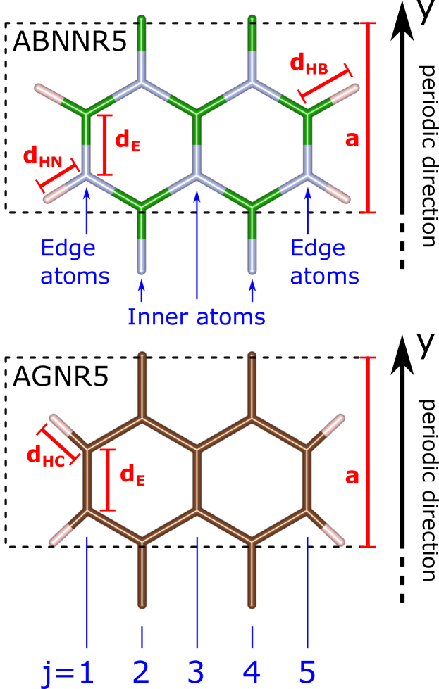
All nanoribbons studied in this article have armchair edges passivated with H atoms. They form an infinite periodic structure in the direction and are confined along . The extension of the periodic cell along is the cell parameter , while the width is expressed by the number which indicates the number of dimers aligned along inside the unitary cell (number of rows). To indicate a specific structure we will attach the index after the label of the material, as in Figure 1, so for instance AGNR5 designates an armchair graphene nanoribbon of size .
Density functional theory calculations were carried out within the generalized gradient approximation using the PBE Perdew et al. (1996) exchange correlation potential as implemented in the Quantum ESPRESSO Giannozzi et al. (2009) simulation package. Long-range van der Waals corrections were included via the DFT-D2 method Grimme (2006). To avoid interactions between consecutive cells, we included 15 Å and 20 Å of empty space in the and directions respectively. In electron density calculations and relaxation runs, the periodic axis was sampled with 20 k-points centered in (corresponding to 11 irreducible k-points). This mesh was dense enough to converge total energies in the smallest nanoribbons. For density of states (DOS) calculations, a five times denser sampling was adopted for all systems and the resulting spectra have been broadened with a Gaussian distribution with a width of eV.
We used norm-conserving pseudopotentials Hamann (2013) and set the kinetic energy cutoff at 80 Ry in both materials. It is worth stressing that using a large vertical empty space and a high energy cutoff is essential even in the relaxation runs in order to prevent nearly free-electron states from hanging below the states hence jeopardizing the gap description. In fact, as already well known for free-standing layers Posternak et al. (1983, 1984); Blase et al. (1995); Paleari (2019); Latil et al. (2022) and nanotubes Blase et al. (1994a, b); Hu et al. (2010) in BN nanomaterials there is a competition at the bottom conduction between and states, whose right alignment requires a dedicated convergence study. If sometimes one can overlook this issue in BN layers, because the two competing states originate direct and indirect band gaps, this is not the case in ABNNRs where both states give rise to a direct gap at .
In non-relaxed structures, all atoms occupy the sites of a regular honeycomb lattice with an inter-atomic distance of 1.42 Å. Structural relaxation runs have been performed with the Broyden–Fletcher–Goldfarb–Shanno (BFGS) algorithm for all systems with the stopping criterion of all forces being lower than eV/Å. We allowed variations of the cell parameter and all atomic positions. As clarified in the following, we also run some calculations letting only specific atoms to move. In Figure 1 we report the relaxed structures of AGNR and ABNNR at for sake of example, and we introduce some notable structural parameters. In the AGNRs, the main modifications with respect to non-relaxed structures are a contraction of the distance between edge atoms and between C and H . In ABNNR, we observe a similar contraction of the B-N distance on the edges , and different contractions of the distances between H-B and H-N (). We observed also that these modifications are basically independent on the size of the nanoribbon both qualitatively and quantitatively, so the structural parameters undergo minimal variations when comparing nanoribbons of different size.
III Gap edge states
III.1 AGNRs
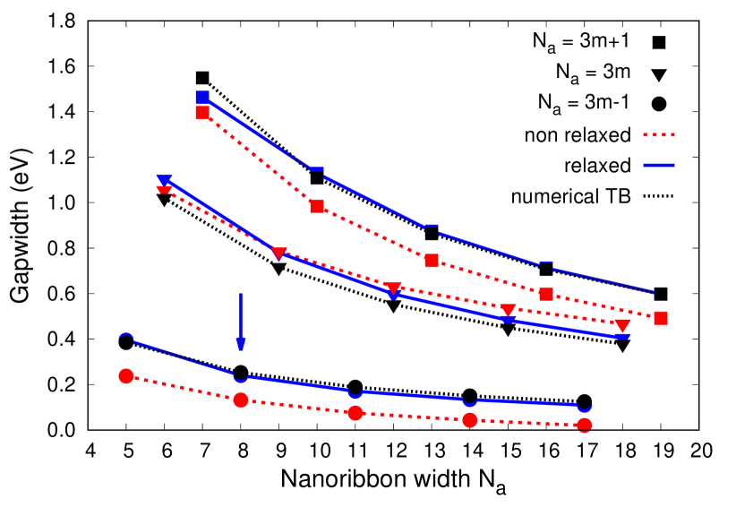
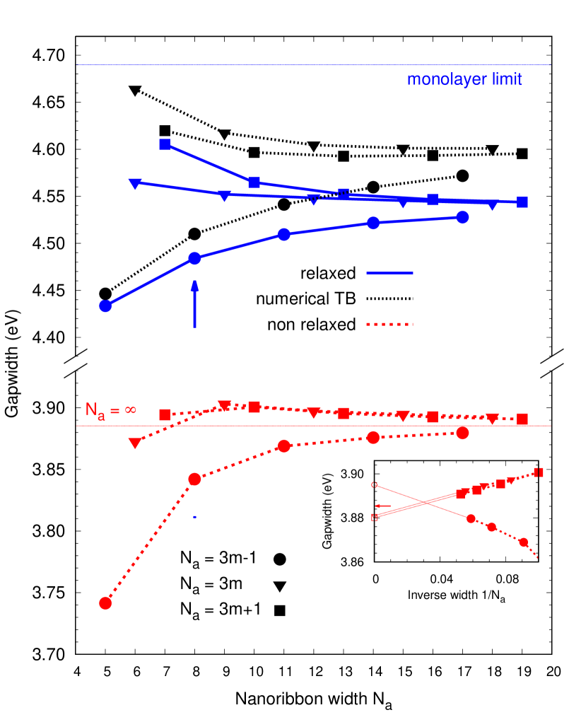
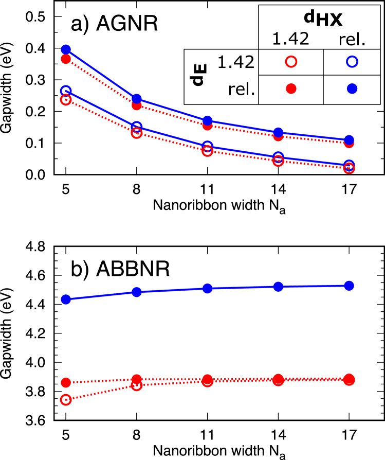
The electronic structure of AGNRs has been already studied in the past Ezawa (2006); Nakada et al. (1996); Behzad and Chegel (2018); Wakabayashi et al. (1999); Yang et al. (2007); Osella et al. (2012); Saraswat et al. (2021); Nematian et al. (2012); Barone et al. (2006); Jha et al. (2019); Nishad et al. (2020); Lu et al. (2009); Prabhakar and Melnik (2019); Ren et al. (2007). Both non-relaxed and relaxed ribbons display a band gap at of gapwidth . Because of the 1D confinement, the gapwidth falls in one of the three families , or (with ). Each family follows a different trend which asymptotically tends to zero for growing nanoribbon sizes and follows the general rule . This is depicted in Figure 2 where we plot the gapwidth of AGNRs versus for both non-relaxed and relaxed structures (red dashed and solid blue curves). The effect of relaxation is to open the gap by about 0.1 eV in families and , while in the the opening is observed only in small nanoribbons, while the gap closes in larger ones. Our results are in quantitative agreement with previous works both for relaxed Son et al. (2006); Yang et al. (2007); Ren et al. (2007); Barone et al. (2006), and unrelaxed simulationsLu et al. (2009).
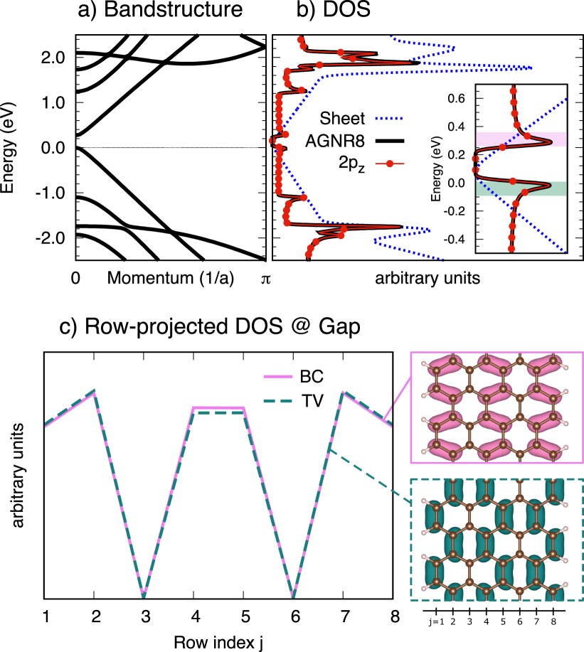
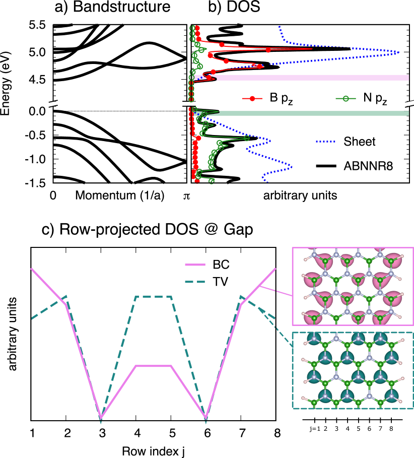
To characterise better the gap states, we analyzed in more detail the nature of the TV and the BC states at in the relaxed structures. In panels a) and b) of Figure 3, we report the band structure and the density of states (DOS) of the AGNR8, chosen as a representative example. For sake of comparison, in panel b) we also report the orbital-projected DOS and the DOS of an infinite graphene sheet with the same inter-atomic distance. The DOS around the gap (from -1.5 eV to 1.5 eV) displays neat van Hove singularities arranged more or less symmetrically with respect to the middle of the gap. As the inset of panel b) shows clearly, the states composing the gap are entirely of character. They form a bonding with nodes on the plane, as expected. Instead, the first empty state is found at 3 eV above the BC. To go deeper in the analysis of the gap-edge states, we look at the site-projected DOS. We integrated the bare data inside an interval of 0.1 eV encompassing the TV and BC (shaded bands in the instet of Figure 3b). The outcome of this analysis is summarised in Figure 3c), where the site-projected DOS of gap-edge states is reported as a function of the row index (note that the curves are plotted on the same axis). At variance from what observed in zigzag nanoribbons Fujita et al. (1996), the gap states are not concentrated on the edge atoms, but rather delocalized throughout the full nanoribbon and present a modulation that nicely displays the characteristics of a static wave. This observation is confirmed by the wave-like modulation of the charge probability associated with the TV and BC states, reported aside panel c). The wavefunction plot shows also that there is no spill-out on the passivating hydrogens and that, with respect to the edge-bbondings , TV and BC states display respectively a bonding and an antibbonding character.
III.2 ABNNRs
The gapwidth of ABNNRs fall in the same three families with the same hierarchyZhang and Guo (2008); Li et al. (2010); Topsakal et al. (2009). This similarity with the graphene ribbons is actually quite general and can be understood from a simple tight-binding model (see section IV.2). The evolution of the ABNNRs gapwidth for sizes going from =5 to 19 in the relaxed and non-relaxed configurations is presented in Figure 4 by the solid blue and the red dashed lines. The non-relaxed structures present a gap that monotonically tends to the limit in a way that is similar to non-passivated calculationsTopsakal et al. (2009). We estimate eV from the weighted average of the curves extrapolated at (cfr. inset of the Figure). This value is about 0.8 eV lower than the gapwidth of the isolated BN sheet (4.69 eV in PBE). All these aspects are consistent because, as it will become clearer later, in non-relaxed calculation, H atoms are too far to saturate efficiently the dangling bonds located at the edges of the ribbbon. As a consequence, these form edge states inside the gap that lower the gapwidth similarly to what happens in non-passivated (bare) ribbons.
As a result of the structural optimisation, the gapwidth of all families opens and tends to an asymptotic limit that is still about 0.1 eV lower than in the isolated monolayer, in agreement with similar calculations Park and Louie (2008); Topsakal et al. (2009). This discrepancy is ascribed to a non-negligible edge contribution to the BC state, obviously absent in the isolated monolayer (cfr. the row-projected DOS analysis here below, andPark and Louie (2008)). Finally, we note that the first empty state, i.e. the near free-electron state, is only 0.5 eV above the BC.
Similarly to what done before, in Figure 5 we report the band structure, the projected DOS and the row-resolved DOS of the TV and BC states of the representative ABNNR8 system. We verify that the TV and the BC states are formed essentially of N-centered and B-centered orbitals respectively. The row-projected DOS of both TV and BC, reported in panel c), shows again a very nice static-wave-like modulation with nodes in rows 3 and 6, but at vairance with the AGNR8 case, here the TV and BC states localize differently: while the TV states are delocalised on the entire nanoribbon as in the previous case, the BC states are clearly peaked at the edges. The visualization of the associated charge density confirms that the TV state is characterised by a wavefunction equally delocalised on all the N atoms except those on rows 3 and 6. Instead, the BC state presents a wavefunction more concentrated on the edge B atoms with non negligible tails touching passivating H and edge nitrogens, in contrast to the isolated monolayer.
The compared study of the TV and BC states of AGNRs and ABNNRs suggests that the gap of the two materials responds differently to modifications of the morphology and the passivation of the edges. To test this intuition, we have performed a detailed analysis by separating the two effects.
IV Morphology VS Chemistry of the edges
IV.1 Distinguishing the effects through selective relaxation in DFT
Several investigations can be found in literature on the effects of edge reconstruction on the gapwidth of AGNR and ABNNREzawa (2006); Son et al. (2006); Barone et al. (2006); Ding et al. (2009); Jha et al. (2019); Nishad et al. (2020); Topsakal et al. (2009); Prabhakar and Melnik (2019); Lu et al. (2009); Ren et al. (2007). However, a study that systematically compares the effects of passivation and edge morphology is absent. Here we monitor the gapwidth in the family by relaxing separately the H-X distances ( = C, B or N) and the C-C or B-N distance on the edges . We did calculate data from the other two families but we do not report them because they have qualitatively the same behaviour.
In Figure 6, a variation of is represented by a change in the line’s type (color and dash), while a variation of is represented by a change in the symbols (colour filled or empty). Let us examine first the case of AGNRs in panel a). We can start from a non-relaxed configuration where all atoms are equidistant ==1.42 Å (empty bullets, red dashed line), then we reduce to its relaxed value 1.08 Å (empty bullets, blue solid line). We observe that there is basically no variation on the AGNRs’ gapwidth. Instead, contracting the edge bonds from =1.42 Å to =1.36 Å opens the gap by around 0.15 eV irrespective of the value of . Consequently, we conclude that in AGNRs, the variations of the gapwidth induced by the relaxation and reported in Figure 2 are essentially due to changes of bond length between C atoms at the edge. Interestingly, this gap opening is approximately independent on the width of the ribbon.
Passing now to the study of ABNNRs (bottom panel), we observe an opposite behaviour. The gapwidth undergoes very small changes upon relaxation of , whereas the passage from the unrelaxed H-B and H-N distance (1.42 Å) to the relaxed values clearly opens the gap by about 0.8 eV. To be more precise, by changing separately the two distances and (not shown), we found that it is the bonding between H and B that plays a major role in the opening of the gapwidth, indicating a dominant contribution from conduction states consistently with the observations we drew from Figure 5. According to this analysis, the gapwidth of ABNNRs is more sensitive to the passivation than to the very morphology of the edge. Once again we notice that the gap opening is basically independent on . This clarifies why our non-relaxed DFT gapwidth look very similar to the non-passivated results of Topsakal and coworkers Topsakal et al. (2009).
IV.2 Unperturbed tight-binding model
To investigate further the reasons of this different behaviour, we generalise a ladder tight-binding model introduced initially for AGNRs to the heteroatomic case. Changes in the edge passivation and morphology will be successively introduced through variations of the on-site and hopping parameters of the model, as suggested in Ezawa (2006); Son et al. (2006), and the modified Hamiltonian solved both numerically and perturbativelySon et al. (2006).
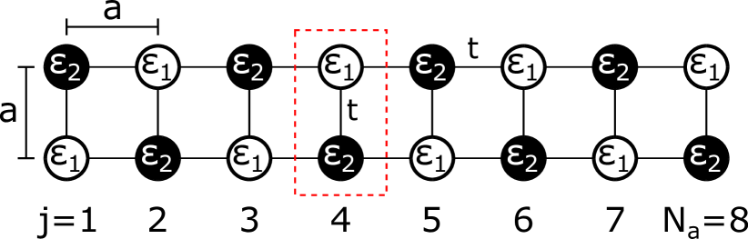
Following references Ezawa (2006); Fujita et al. (1996); Nakada et al. (1996); Wakabayashi et al. (1999); Son et al. (2006); Shyu (2014); Nematian et al. (2012), the gap of an armchair nanoribbon whose TV and BC states are formed of orbitals can be described with a ladder tight-binding model as the one reported in Figure 7. The Hamiltonian of the model reads:
| (1) |
The index labels the position of a dimer in the coordinate (row coordinate), while indicates the atomic site within the dimer ( or in AGNRs and or in ABNNRs). The basis function is the orbital of the atom of the dimer placed at . For , is centered on the bottom rung if is odd and in the upper rung if is even, and the opposite for .
At the unperturbed level, does not depend on the row-index and is equal to for and for , with . In the first-neighbour approximation, the hopping term if and and vanishes otherwise. The unperturbed solutions of this model are:
| (2) |
where , the discrete index comes from the confinement in the direction and . The eigenfunction associated to these states read
| (3) |
with
| (4) |
where the function if and if . At this point, it is worth stressing two aspects. First, if one poses , then the Hamiltonian becomes diagonal and equivalent to that of a non-interacting system. Consistently, the coefficients become those of a pure system: and . If instead one takes the homoatomic limit, i.e. , then the coefficients become a bonding and antibonding pair, with and .
The last occupied state (TV) and the first empty state (BC) are found at the integer quantum number that minimizes the quantity , i.e. that minimize . If or with , then . Note that the interacting term changes sign in passing from one family to the other. Instead if , then the integer and . These considerations leads to the unperturbed gap of a heteroatomic system ():
| (7) |
and the eigenstates of the TV and BC of the family are pure states. The gap of a homoatomic system () reads:
| (10) |
and the eigenstates of the TV and BC of the family are the bonding and antibonding combinations of and .
IV.3 Distinguishing the effects through perturbation theory
As inEzawa (2006); Son et al. (2006), we now add to a perturbation Hamiltonian which consists in adding to the hopping term connecting the atoms of the edge rows () and in changing their on-side energy by . The hopping perturbation accounts for changes in , so it is more strongly related to the edge morphology, while the on-site one takes into account variations of and of the passivating species. The perturbative correction to the energy of the generic state reads
| (11) |
In the heteroatomic case , the perturbative correction to the gap is always . Using (11), the coefficients (4) or their appropriate limit, and remembering that , then the gap correction for the case reads,
| (12) |
for ; and
| (13) |
for and . Notice that, by construction, is the closest to zero among the accessible values, so the term is always negligible. The result shows that in ABNNRs the variations of the gap are mostly due to the chemical environment of the edge atoms. This dependence comes ultimately from an interference between the TV and the BC wavefunctions. These two states are very close to pure states, so the mixed products and of equation (11) are systematically negligible, and they do actually vanish in the family where the two states are perfectly pure.
In the homoatomic case () the corrected gap can be obtained following the same approach as before, and taking the appropriate limits of the coefficients (4). However, more attention must be paid in studying the family . In fact this case corresponds to the double limit and . Even though the final eigenvalues do not depend on the order with which the two limits are taken, the eigenstates do, therefore also the perturbative corrections depend on this choice. In DFT calculation and experiments, the system itself is well defined at the very first place, because one works either with ABNNRs or with AGNRs. So, for comparisons with DFT to make sense, the right order with wich the limits must be taken is: first , followed by . Finally, one has to pay attention to another point: in the family, the TV and the BC states are degenerate and the unperturbed gap is 0. So there is no reason to define rather than its opposite. However, the correction must be positive, so the correction must be defined as the modulus of the difference above. Putting all these things together, one gets for the homoatomic () case
| (14) |
This result shows that in AGNRs most of the variations of the gap is accounted by , so by morphological changes of the bonding between edge atoms, and not by changes of their chemical environment. Once again this result can be understood from the symmetries of the TV and BC wavefunctions. In fact, when , the TV and BC states are perfect bonding and antibonding combinations at any , so their difference causes the terms in of equation (11) to always cancel out. This result, although in perfect agreement withSon et al. (2006), seems to be in blatant contradiction with results from 2H-passivated AGNRsLu et al. (2009), where the gap is found independend on the C-C edge distance. Actually, these systems present a hybridisation of the type and their gapwidth can not be described by this model.
IV.4 Validitation of the perturbative approach
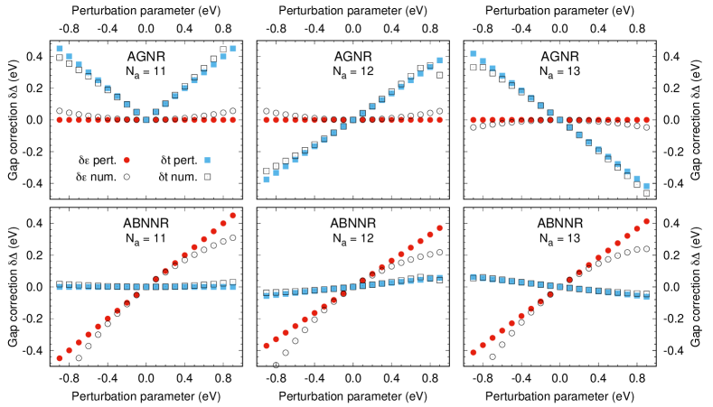
Besides the perturbative approach, we also solved the perturbed Hamiltonian numerically. For the unperturbed problem, we parametrized the model with values that fit the band structure of the isolated graphene and hBN monolayers. Instead, the perturbation parameters and have been adjusted to recover as best as possible the DFT curves reported in Figures 2 and 4. The best parameters are reported in Table 1. Successively we explored how the gap changes upon variations of the perturbative parameters and in the range -1 eV, +1 eV in the nanoribbons of width =11, 12 and 13, i.e. one representative nanoribbon per family. Guided by physical intuitions we took in the case of AGNRs, and in the case of ABNNRs.
Globally, the numerical and the perturbative gapwidth are in very good agreement for both ABNNRs and AGNRs in the range explored, confirming our conclusions. In all cases, the numerical solution displays a quadratic trend with respect to which adds on top of the invariance (AGNR) or the linear (ABNNR) dependence predicted by the perturbative approach. The deviations between the two approaches are larger for this parameter than for , with the larger deviations of the order of 0.2 eV in the and families of ABNNRs. Instead, the deviations for the parameter are in general very small and never larger than 0.1 eV. Note however that for extreme values of , the numerical solution may undergo a band crossing in the top valence and the bottom conduction which would lead to a sudden closing of the gap, as it is the case at in AGNR13 and in AGNR12. This physics is not accessible in our first order expansion and clearly sets the limit of applicability of the perturbative approach.
V Conclusion
We have calculated with DFT the gapwidth of graphene and boron nitride armchair nanoribbons (AGNRs and ABNNRs) for ribbon sizes going from rows to rows both for relaxed and unrelaxed structures. We have relaxed selectively specific interatomic distances and reported how the gapwidth changes upon variations of the bondlength with passivating atoms (chemistry-driven changes) and between edge atoms (morphology-driven changes). Thanks to this selective relaxation, we showed that the variations of the gapwidth in AGNRs are morphology-driven, while in ABNNRs are chemistry-driven. To understand why, we adopted and extended the tight-binding approach introduced by Son and coworkers Son et al. (2006) and we demonstrated that the interference between the wavefunctions of the top valence and the bottom conduction are at the origin of these two distinct responses.
In the AGNR case, these states are basically a bonding and antibonding pair. As the two states are equally distributed on the atoms, the difference between BC and TV leads to a mutual cancellation of on-site changes, and only hopping terms survive. This explains the stronger dependence of the gapwidth on interatomic distances and hence on the morphology of the edges rather than the chemical environment. At variance, in ABNNR case, the TV and the BC states are basically pure states and the effective Hamiltonian is quasi non-interacting. As a result, the two states are mostly insensitives to variations in the hopping term and are instead strongly affected by on-site variations (chemical environment).
Our results can help pushing further the research on nanoribbon-based devices, as they clarify the role played by edge-engineering, and selective passivation and provide the tools to investigate more complex scenarios.
References
- Geim and Novoselov (2007) A. K. Geim and K. S. Novoselov, Nature Materials 6, 183 (2007).
- Watanabe et al. (2009) K. Watanabe, T. Taniguchi, T. Niiyama, K. Miya, and M. Taniguchi, Nature Photonics 3, 591 (2009).
- Castro Neto et al. (2009) A. H. Castro Neto, F. Guinea, N. M. R. Peres, K. S. Novoselov, and A. K. Geim, Reviews of Modern Physics 81, 109 (2009), arXiv:0709.1163 .
- Weng et al. (2016) Q. Weng, X. Wang, X. Wang, Y. Bando, and D. Golberg, Chemical Society Reviews 45, 3989 (2016).
- Zhang et al. (2017) K. Zhang, Y. Feng, F. Wang, Z. Yang, and J. Wang, Journal of Materials Chemistry C 5, 11992 (2017).
- Ezawa (2006) M. Ezawa, Phys. Rev. B 73, 045432 (2006).
- Fujita et al. (1996) M. Fujita, K. Wakabayashi, K. Nakada, and K. Kusakabe, Journal of the Physical Society of Japan 65, 1920 (1996).
- Nakada et al. (1996) K. Nakada, M. Fujita, G. Dresselhaus, and M. S. Dresselhaus, Phys. Rev. B 54, 17954 (1996).
- Behzad and Chegel (2018) S. Behzad and R. Chegel, Diamond and Related Materials 88, 101 (2018).
- Wakabayashi et al. (1999) K. Wakabayashi, M. Fujita, H. Ajiki, and M. Sigrist, Physical Review B 59, 8271–8282 (1999).
- Yang et al. (2007) L. Yang, C.-H. Park, Y.-W. Son, M. L. Cohen, and S. G. Louie, Physical Review Letters 99, 186801 (2007), arXiv:0706.1589 .
- Son et al. (2006) Y.-W. Son, M. L. Cohen, and S. G. Louie, Physical Review Letters 97, 216803 (2006).
- Nakamura et al. (2005) J. Nakamura, T. Nitta, and A. Natori, Phys. Rev. B 72, 205429 (2005).
- Park and Louie (2008) C.-H. Park and S. G. Louie, Nano Letters 8, 2200 (2008), pMID: 18593205, https://doi.org/10.1021/nl080695i .
- Wang et al. (2011) S. Wang, Q. Chen, and J. Wang, Applied Physics Letters 99, 063114 (2011).
- Shyu (2014) F.-L. Shyu, Physica B: Condensed Matter 452, 7 (2014).
- Topsakal et al. (2009) M. Topsakal, E. Aktürk, and S. Ciraci, Physical Review B 79, 115442 (2009).
- Zhang and Guo (2008) Z. Zhang and W. Guo, Physical Review B 77, 075403 (2008).
- Ding et al. (2009) Y. Ding, Y. Wang, and J. Ni, Applied Physics Letters 94, 233107 (2009).
- Nematian et al. (2012) H. Nematian, M. Moradinasab, M. Pourfath, M. Fathipour, and H. Kosina, Journal of Applied Physics 111, 093512 (2012).
- Barone et al. (2006) V. Barone, O. Hod, and G. E. Scuseria, Nano Letters 6, 2748 (2006).
- Jha et al. (2019) K. K. Jha, N. Tyagi, N. K. Jaiswal, and P. Srivastava, Physics Letters A 383, 125949 (2019).
- Nishad et al. (2020) V. K. Nishad, A. K. Nishad, S. Roy, B. K. Kaushik, and R. Sharma, Proceedings of the IEEE Conference on Nanotechnology 2020-July, 155 (2020).
- Prabhakar and Melnik (2019) S. Prabhakar and R. Melnik, Physica E: Low-dimensional Systems and Nanostructures 114, 113648 (2019).
- Ren et al. (2007) H. Ren, Q. Li, H. Su, Q. W. Shi, J. Chen, and J. Yang, arXiv , 0711.1700 (2007), arXiv:0711.1700 .
- Lu et al. (2009) Y. Lu, R. Wu, L. Shen, M. Yang, Z. Sha, Y. Cai, and Y. Feng, Applied Physics Letters 94, 122111 (2009).
- Raza and Kan (2008) H. Raza and E. C. Kan, Phys. Rev. B 77, 245434 (2008).
- Li et al. (2010) J. Li, L. Z. Sun, and J. X. Zhong, Chinese Physics Letters 27, 077101 (2010).
- Zheng et al. (2013) P. Zheng, S. E. Bryan, Y. Yang, R. Murali, A. Naeemi, and J. D. Meindl, IEEE Electron Device Letters 34, 707 (2013).
- Murali et al. (2009) R. Murali, Y. Yang, K. Brenner, T. Beck, and J. D. Meindl, Applied Physics Letters 94, 243114 (2009).
- Das et al. (2021) S. Das, S. Bhattacharya, D. Das, and H. Rahaman, AIMS Materials Science 8, 247 (2021).
- Marmolejo-Tejada and Velasco-Medina (2016) J. M. Marmolejo-Tejada and J. Velasco-Medina, Microelectronics Journal 48, 18 (2016).
- Saraswat et al. (2021) V. Saraswat, R. M. Jacobberger, and M. S. Arnold, ACS Nano 15, 3674 (2021).
- Osella et al. (2012) S. Osella, A. Narita, M. G. Schwab, Y. Hernandez, X. Feng, K. Mullen, and D. Beljonne, ACS nano 6, 5539 (2012).
- Mehdi Pour et al. (2017) M. Mehdi Pour, A. Lashkov, A. Radocea, X. Liu, T. Sun, A. Lipatov, R. A. Korlacki, M. Shekhirev, N. R. Aluru, J. W. Lyding, V. Sysoev, and A. Sinitskii, Nature Communications 8, 820 (2017).
- Schwab et al. (2015) M. G. Schwab, A. Narita, S. Osella, Y. Hu, A. Maghsoumi, A. Mavrinsky, W. Pisula, C. Castiglioni, M. Tommasini, D. Beljonne, X. Feng, and K. Müllen, Chemistry – An Asian Journal 10, 2134 (2015), https://onlinelibrary.wiley.com/doi/pdf/10.1002/asia.201500450 .
- Wang et al. (2016) G. Wang, S. Wu, T. Zhang, P. Chen, X. Lu, S. Wang, D. Wang, K. Watanabe, T. Taniguchi, D. Shi, R. Yang, and G. Zhang, Applied Physics Letters 109, 053101 (2016), https://doi.org/10.1063/1.4959963 .
- Dauber et al. (2014) J. Dauber, B. Terrés, C. Volk, S. Trellenkamp, and C. Stampfer, Applied Physics Letters 104, 083105 (2014), https://doi.org/10.1063/1.4866289 .
- Huang et al. (2009) B. Huang, M. Liu, N. Su, J. Wu, W. Duan, B.-l. Gu, and F. Liu, Phys. Rev. Lett. 102, 166404 (2009).
- Huang et al. (2012) B. Huang, H. Lee, B. L. Gu, F. Liu, and W. Duan, Nano Research 5, 62 (2012).
- Perdew et al. (1996) J. P. Perdew, K. Burke, and M. Ernzerhof, Physical Review Letters 77, 3865 (1996).
- Giannozzi et al. (2009) P. Giannozzi, S. Baroni, N. Bonini, M. Calandra, R. Car, C. Cavazzoni, D. Ceresoli, G. L. Chiarotti, M. Cococcioni, I. Dabo, et al., Journal of physics: Condensed matter 21, 395502 (2009).
- Grimme (2006) S. Grimme, Journal of Computational Chemistry 27, 1787 (2006), https://onlinelibrary.wiley.com/doi/pdf/10.1002/jcc.20495 .
- Hamann (2013) D. R. Hamann, Phys. Rev. B 88, 085117 (2013).
- Posternak et al. (1983) M. Posternak, A. Baldereschi, A. J. Freeman, E. Wimmer, and M. Weinert, Phys. Rev. Lett. 50, 761 (1983).
- Posternak et al. (1984) M. Posternak, A. Baldereschi, A. J. Freeman, and E. Wimmer, Phys. Rev. Lett. 52, 863 (1984).
- Blase et al. (1995) X. Blase, A. Rubio, S. G. Louie, and M. L. Cohen, Physical Review B 51, 6868 (1995).
- Paleari (2019) F. Paleari, First-principles approaches to the description of indirect absorption and luminescence spectroscopy: exciton-phonon coupling in hexagonal boron nitride, Ph.D. thesis, University of Luxembourg (2019).
- Latil et al. (2022) S. Latil, H. Amara, and L. Sponza, “Structural classification of boron nitride twisted bilayers and ab initio investigation of their stacking-dependent electronic structure,” (2022), accepted in SciPost Physics.
- Blase et al. (1994a) X. Blase, L. X. Benedict, E. L. Shirley, and S. G. Louie, Phys. Rev. Lett. 72, 1878 (1994a).
- Blase et al. (1994b) X. Blase, A. Rubio, S. G. Louie, and M. L. Cohen, Europhysics Letters (EPL) 28, 335 (1994b).
- Hu et al. (2010) S. Hu, J. Zhao, Y. Jin, J. Yang, H. Petek, and J. G. Hou, Nano Letters 10, 4830 (2010), pMID: 21049977, https://doi.org/10.1021/nl1023854 .