Influence of atomic relaxations on the moiré flat band wavefunctions in antiparallel twisted bilayer WS
Abstract
Twisting bilayers of transition metal dichalcogenides (TMDs) gives rise to a periodic moiré potential resulting in flat electronic bands with localized wavefunctions and enhanced correlation effects. In this work, scanning tunneling microscopy is used to image a WS2 bilayer twisted approximately off the antiparallel alignment. Scanning tunneling spectroscopy reveals the presence of localized electronic states in the vicinity of the valence band onset. In particular, the onset of the valence band is observed to occur first in regions with a Bernal stacking in which S atoms are located on top of each other. In contrast, density-functional theory calculations on twisted bilayers which have been relaxed in vacuum predict the highest lying flat valence band to be localized in regions of AA’ stacking. However, agreement with the experiment is recovered when the calculations are carried out on bilayers in which the atomic displacements from the unrelaxed positions have been reduced reflecting the influence of the substrate and finite temperature. This demonstrates the delicate interplay of atomic relaxations and the electronic structure of twisted bilayer materials.
*These authors contributed equally
When a pair of two-dimensional (2D) materials are stacked vertically and then rotated relative to each other, a moiré superlattice is created. Electrons in such a superlattice experience a moiré potential which favors electron localization in specific stacking regions, reduces the electrons’ kinetic energy, and results in the formation of flat bands with enhanced electron-electron interactions, promoting phenomena such as superconductivity, Mott insulating phases, topological phases, coupled spin-valley states, and interlayer excitons.1, 2, 3, 4, 5, 6, 7
In contrast to graphene bilayers which exhibit flat bands at a specific “magic” twist angle, bilayers of transition metal dichalcogenides (TMDs) offer a much larger range of twist angles at which flat bands are realized8, 9, 10, 11, 12, 13, 14, opening broader possibilities for creating previously inaccessible correlated systems. Both TMD homobilayers (in which two layers of the same material are combined) and heterobilayers (in which two different TMD monolayers are combined) have been studied. In heterobilayers, the length scale of the moiré pattern is less sensitive to the twist-angle than in homobilayers, leading to reduced twist angle disorder in large samples. As a result, to date, several heterobilayer TMDs such as WSe2/WS2 11, 15, MoS2/WS2 16, 17, 18, 19, MoS2/WSe220, 13 and WSe2/MoSe2 21 have been investigated experimentally, with reports of correlated phenomena such as superconductivity, Mott insulating phases, generalized Wigner crystals, etc.22, 9, 23, 11. Moiré patterns of TMD homobilayers are highly sensitive to the twist angle, and thus expected to exhibit more twist-angle disorder. As a consequence, these systems are less studied despite having great potential for inducing strong moiré potentials 8, 24, 3, 30, 26. For example, recent scanning probe microscopy experiments on a WSe2/WSe2 homobilayer have demonstrated twist-angle-dependent lattice reconstructions near a twist angle resulting in multiple energy-separated ultra-flat valence bands for long moiré wavelengths (6 nm-12 nm).10
Semiconducting TMDs have metal and chalcogen atoms occupying the lattice sites in their unit cell breaking sub-lattice symmetry. For this reason, twisted TMD bilayers fall into two classes: parallel (P) aligned bilayers with a zero twist angle close to , and antiparallel (AP) aligned bilayers with twist angles near . These two classes exhibit different stacking configurations in the moiré unit cell which results in different atomic relaxations in the form of both out-of-plane buckling and in-plane reconstructions. In-plane reconstructions can be understood as the result of the layers deforming to increase the area of the energetically preferred stacking order. 27, 24, 28, 8 For very small twist angles (or twist angles very close to ), this reconstruction produces networks of uniform stacking order domains separated by highly strained domain walls. In the case of P-aligned TMD homobilayers, the system tends towards a network of triangular stacking order domains. Due to the lack of inversion symmetry, these domains host interlayer charge transfer leading to an out-of-plane ferroelectric dipole moment.24, 21, 27, 29 In the case of AP-aligned TMD homobilayers, no such charge transfer occurs. While AP systems do form domain wall networks at angles very close to , they generally exhibit less pronounced in-plane reconstructions than P-aligned bilayers at a given twist-angle offset, leading to a more smoothly varying periodic lattice distortion over the moiré unit cell. 25 In all cases, both out-of-plane buckling and in-plane reconstruction have a profound impact on the electronic properties of TMD homobilayers. In-plane and out-of-plane deformations cause the simple band-folding description of a moiré pattern band-structure to break down, for example, causing a modification in the real-space position of the valence band edge wavefunctions. Strain is furthermore critical to wavefunction localization responsible for strong correlated effects observed in these systems. 8, 24
As the field of moiré-induced flat band physics progresses, it is important to explore a larger range of homobilayer systems, especially using scanning probe techniques that can directly reveal the local twist angle. Here, we report room temperature scanning tunnelling microscopy/spectroscopy (STM/STS) studies of moiré superlattices of 6 nm wavelength in the WS2/WS2 bilayer system near twist angle or antiparallel (AP) alignment, together with extensive large-scale density-functional theory calculations. Importantly, we demonstrate that the localization of the flat-band wavefunctions depends sensitively on the degree of lattice relaxations.
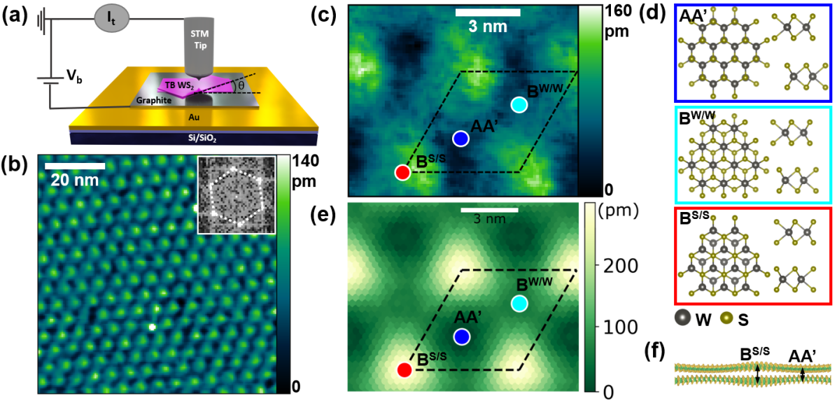
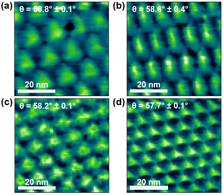
We fabricated the AP-WS2 twisted bilayer using a variation of the “tear-and-stack” dry transfer method (see Methods section) and performed room temperature STM/STS experiments, as indicated schematically in Figure 1(a). Across the entire sample, we identified moiré patterns with a range of periods (6 nm-14 nm) (Supplementary Figure S1), corresponding to a twist-angle range of -, indicating the presence of twist-angle disorder within the AP-WS2 sample. A large area of uniform hexagonal moiré pattern with a period of 6.0 nm 0.2 nm (corresponding to a twist angle of ) is shown in Figure 1(b). A zoomed-in scanning tunnelling micrograph of this pattern in Figure 1(c) highlights the unit cell and the different high-symmetry stacking regions within it (, ’, ), with corresponding atomic configurations described in Figure 1(d).
A simulated STM topograph of a AP-twisted WS2 bilayer obtained from density functional theory (DFT) calculations based on the Tersoff-Hamann approximation 31 is shown in Figure 1(e). Before the DFT calculations, the relaxed atomic positions of the twisted bilayer, shown in Fig. 1(f), were obtained using classical force fields (see Methods). The simulated topograph is in good agreement with the experimental micrograph of Figure 1(c). In particular, the bright regions correspond to stacking. This stacking exhibits the largest buckling and therefore also the largest tunnelling matrix element.
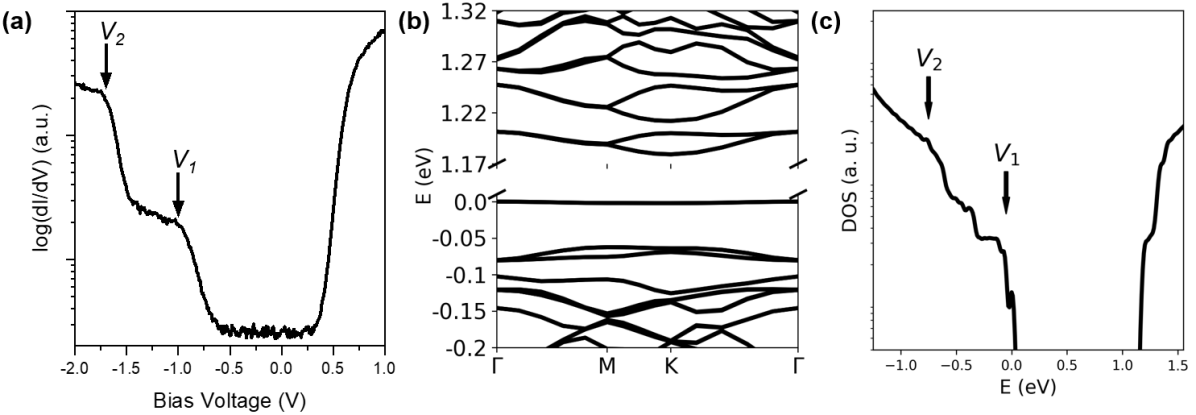
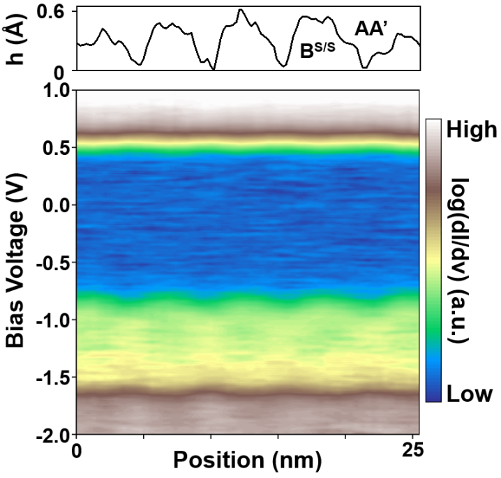
To explore the local electronic properties of the moiré superlattice in Figure 1(b), we performed scanning tunnelling spectroscopy (STS) measurements. In Figure 2(a) we present the average tunnelling conductance (dI/dV) acquired over five moiré periods (Supplementary Figures S2 and S3). Two notable features are present in the spectrum: a first one (denoted V1) near the valence band edge (VBE), with an energy of eV, and a second feature V2 deeper in the valence band at eV.
These two features are also found in the density of states (DOS) calculated using DFT for the relaxed atomic structure, see Fig. 2(c). The energy separation between the two features is found to be 0.7 eV, in excellent agreement with the experimental result. We note that the valence band edge of the calculated DOS is much sharper than in the experiment, which is likely a consequence of thermal broadening.
To understand the origin of the observed features close to the valence band edge, we also present the DFT band structure of the twisted bilayer in Fig. 2(b). This reveals that the highest valence band is extremely flat with a bandwidth of 2 meV. Approximately 60 meV below the highest valence band we find another pair of relatively flat bands which contribute to the sharp feature . We also identify another sharp feature in the DOS 0.7 eV below the , in good agreement with the experiment.
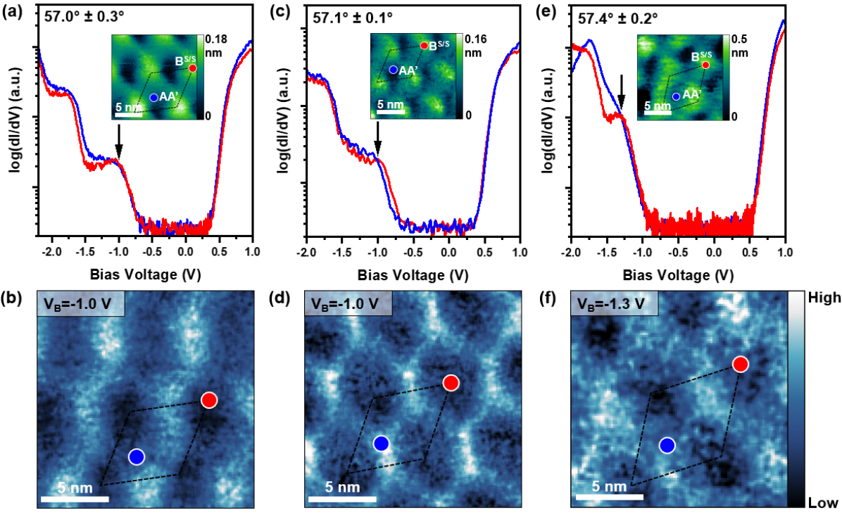
Taking advantage of the spatial resolution of a STM/STS experiment, we measured dI/dV maps corresponding to the feature V1. In Figure 3 we present scanning tunnelling spectra collected at AA’ and stacking regions taken on three areas with slightly different twist angles: [Figure 3(a),(b)], [Figure 3(c),(d)] and [Figure 3(e),(f)]. The insets show the associated topographic image including the high-symmetry points and unit cell. These maps demonstrate that the feature V1 is associated with localized states that form a hexagonal pattern with low intensity on the sites and high intensity on the AA’ sites. The spectra taken at the AA’ and sites show that the valence band onset occurs at the site, suggesting that the highest-lying valence band is localized at this site (indicating that the localized state associated with V1 is not the highest lying valence band). While this difference between the two sites is clearly visible for the system, the separation between the two spectra is much smaller for the other two systems (for the system the onsets at the AA’ and the sites occur almost at the same energy). We also note that more significant differences between the various twist-angle regions are found further away from the valence band onset indicating that the electronic structure is highly sensitive to the local twist angle.
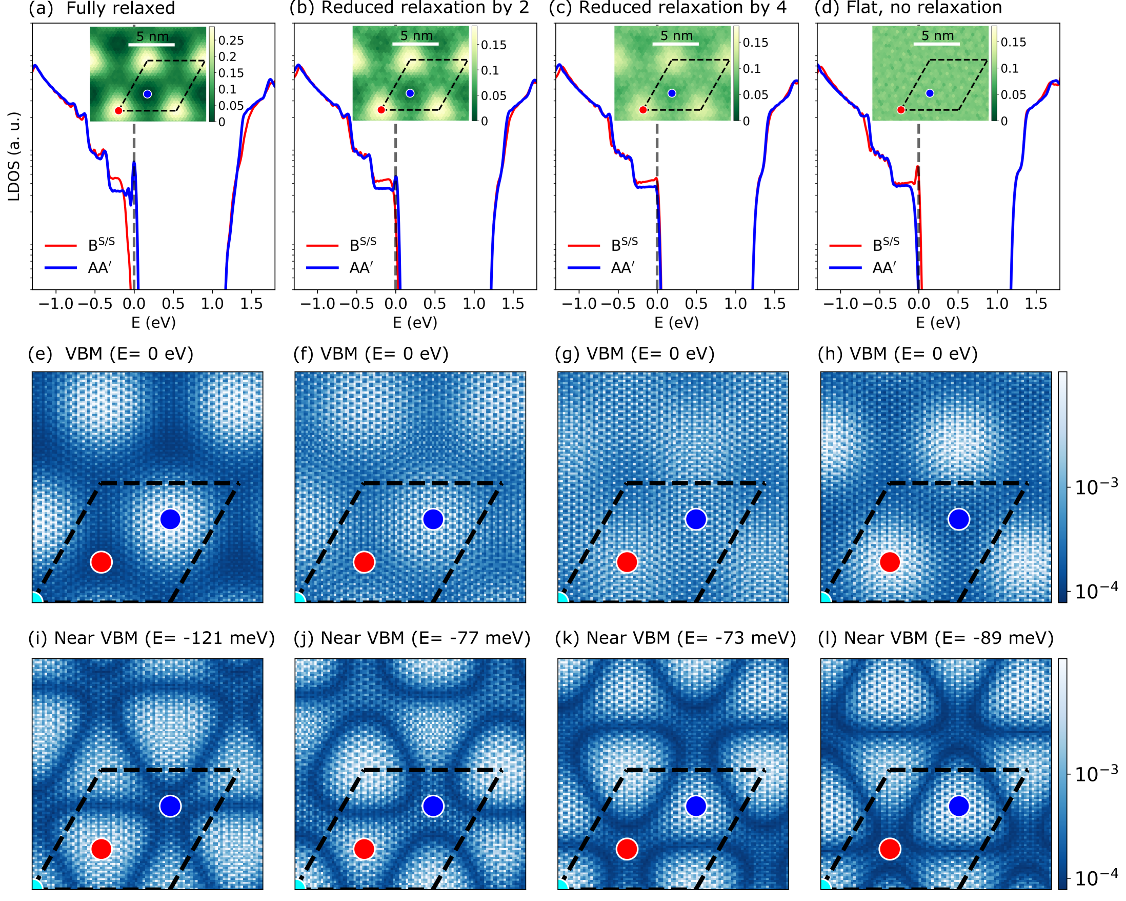
To further understand the experimental findings, we calculated the local density of states (LDOS) at the AA’ and sites using DFT (see SI for more details). Figure 4(a) shows the result for a fully relaxed free-standing twisted bilayer (i.e. a bilayer in free space without a substrate). In the inset of Fig. 4(a), we also show the calculated STM topography. The LDOS in Figure 4(a) suggests that in this scenario the highest valence band is highly localized at the ’ sites, contrary to the experimental findings of Figure 3. Interestingly, the highest valence band is localized on the site when no atomic relaxations are included and the layers remain flat, see Fig. 4(d). This suggests that atomic relaxations in the experimental sample are not as strong as in a free-standing system. Possible origins of this discrepancy include (i) the influence of the substrate which is not included in our simulations, (ii) atomic motions due to thermal fluctuations, and (iii) extrinsic strains. To test this hypothesis, we also carry out DFT calculations for twisted bilayers in which the displacements of all atoms from their unrelaxed positions are reduced by a factor of 2 in Fig. 4(b) and by a factor of 4 in Fig. 4(c), compared to their values in the fully relaxed free-standing system. In Figure 4(h) we show the calculation in the absence of relaxation. In these systems, the LDOS in the AA’ and the regions are almost the same near the valence band onset in good agreement with the experimental findings. These results clearly demonstrate the high sensitivity of the electronic structure on atomic relaxations.
Figures 4(e)-(h) demonstrate that the wavefunction of the highest lying valence band does not correspond to the experimental measurement for the feature V1 shown in the lower panel of Fig. 3: the wavefunctions do not form a honeycomb shape, but a triangular pattern. The only exception corresponds to the wavefunctions obtained when all displacements are reduced by a factor of 4, see Fig. 4(g). However, in this case, the dark regions of the honeycomb pattern are not associated with regions as in the experiment. Instead, we have found that a deeper-lying valence band has a low intensity on the Bs/S regions when relaxations are absent or strongly reduced, see Figs. 4(g) and (h). This state also exhibits a six-fold symmetry around these BS/S sites as does the honeycomb pattern observed in experiments. We, therefore, assign the experimental maps of the feature V1 to this deeper-lying valence band. Considering the thermal broadening in this experiment, it is not surprising that the contributions from a single narrow flat band would not be the only ones measured at a particular energy.
In conclusion, we use scanning tunneling microscopy and spectroscopy to characterize the spatial distribution of the wave functions corresponding to flat bands in a bilayer WS2 sample twisted off the antiparallel alignment. To understand the localization at the different high-symmetry stacking regions we performed density-functional theory calculations which revealed that atomic relaxations play a critical role in determining the degree to which the wave functions associated with flat bands localize on the high-symmetry regions. We find that in our samples the atomic relaxations are much suppressed compared to calculations for the idealized system of a bilayer in vaccum. These findings provide insight into the spatial distributions of the wave functions associated with flat bands believed to be responsible for the occurrence of correlated electron phenomena, demonstrating that atomic relaxations are a way to control the localization of the wave functions.
References
- 1 Shimazaki, Y.; Schwartz, I.; Watanabe, K.; Taniguchi, T.; Kroner, M.; Imamoğlu, A. Strongly correlated electrons and hybrid excitons in a moiré heterostructure. Nature 2020, 580, 472–477.
- 2 Yankowitz, M.; Chen, S.; Polshyn, H.; Zhang, Y.; Watanabe, K.; Taniguchi, T.; Graf, D.; Young, A. F.; Dean, C. R. Tuning Superconductivity in twisted bilayer graphene. Science 2019, 363, 1059–1064.
- 3 An, L.; Cai, X.; Pei, D.; Huang, M.; Wu, Z.; Zhou, Z.; Lin, J.; Ying, Z.; Ye, Z.; Feng, X., et al. Interaction effects and superconductivity signatures in twisted double-bilayer WSe2. Nanoscale Horiz. 2020, 5, 1309–1316.
- 4 Brotons-Gisbert, M.; Baek, H.; Molina-Sánchez, A.; Campbell, A.; Scerri, E.; White, D.; Watanabe, K.; Taniguchi, T.; Bonato, C.; Gerardot, B. D. Spin–layer locking of inter-layer excitons trapped in moiré potentials. Nat. Mater. 2020, 19, 630–636.
- 5 Choi, J.; Hsu, W.-T.; Lu, L.-S.; Sun, L.; Cheng, H.-Y.; Lee, M.-H.; Quan, J.; Tran, K.; Wang, C.-Y.; Staab, M., et al. Moiré potential impedes interlayer exciton diffusion in van der Waals heterostructures. Sci. Adv. 2020, 6, eaba8866.
- 6 Tran, K.; Moody, G.; Wu, F.; Lu, X.; Choi, J.; Kim, K.; Rai, A.; Sanchez, D. A.; Quan, J.; Singh, A., et al. Evidence for moiré excitons in van der Waals heterostructures. Nature 2019, 567, 71–75.
- 7 Das, S.; Dandu, M.; Gupta, G.; Murali, K.; Abraham, N.; Kallatt, S.; Watanabe, K.; Taniguchi, T.; Majumdar, K. Highly tunable layered exciton in bilayer WS2: linear quantum confined stark effect versus electrostatic doping. ACS Photonics 2020, 7, 3386–3393.
- 8 Naik, M. H.; Kundu, S.; Maity, I.; Jain, M. Origin and evolution of ultraflat bands in twisted bilayer transition metal dichalcogenides: Realization of triangular quantum dots. Phys. Rev. B 2020, 102, 075413.
- 9 Wang, L.; Shih, E.-M.; Ghiotto, A.; Xian, L.; Rhodes, D. A.; Tan, C.; Claassen, M.; Kennes, D. M.; Bai, Y.; Kim, B., et al. Correlated electronic phases in twisted bilayer transition metal dichalcogenides. Nat. Mater. 2020, 19, 861–866.
- 10 Li, E.; Hu, J.-X.; Feng, X.; Zhou, Z.; An, L.; Law, K. T.; Wang, N.; Lin, N. Lattice reconstruction induced multiple ultra-flat bands in twisted bilayer WSe2. Nat. Commun. 2021, 12, 1–7.
- 11 Li, H.; Li, S.; Naik, M. H.; Xie, J.; Li, X.; Wang, J.; Regan, E.; Wang, D.; Zhao, W.; Zhao, S., et al. Imaging moiré flat bands in three-dimensional reconstructed WSe2/WS2 superlattices. Nat. Mater. 2021, 20, 945–950.
- 12 Vitale, V.; Atalar, K.; Mostofi, A. A.; Lischner, J. Flat band properties of twisted transition metal dichalcogenide homo- and heterobilayers of MoS2, MoSe2, WS2 and WSe2. 2d Mater. 2021, 8, 045010.
- 13 Waters, D.; Nie, Y.; Lupke, F.; Pan, Y.; Folsch, S.; Lin, Y.-C.; Jariwala, B.; Zhang, K.; Wang, C.; Lv, H., et al. Flat bands and mechanical deformation effects in the moiré superlattice of MoS2-WSe2 heterobilayers. ACS Nano 2020, 14, 7564–7573.
- 14 Maity, I.; Maiti, P. K.; Krishnamurthy, H. R.; Jain, M. Reconstruction of moiré lattices in twisted transition metal dichalcogenide bilayers. Phys. Rev. B 2021, 103, L121102.
- 15 Li, H.; Li, S.; Naik, M. H.; Xie, J.; Li, X.; Regan, E.; Wang, D.; Zhao, W.; Yumigeta, K.; Blei, M., et al. Imaging local discharge cascades for correlated electrons in WS2/WSe2 moiré superlattices. Nat. Phys. 2021, 17, 1114–1119.
- 16 Kobayashi, Y.; Yoshida, S.; Sakurada, R.; Takashima, K.; Yamamoto, T.; Saito, T.; Konabe, S.; Taniguchi, T.; Watanabe, K.; Maniwa, Y., et al. Modulation of electrical potential and conductivity in an atomic-layer semiconductor heterojunction. Sci. Rep. 2016, 6, 31223.
- 17 Shi, J.; Tong, R.; Zhou, X.; Gong, Y.; Zhang, Z.; Ji, Q.; Zhang, Y.; Fang, Q.; Gu, L.; Wang, X.; Liu, Z.; Zhang, Y. Temperature-Mediated Selective Growth of MoS2/WS2 and WS2/MoS2 Vertical stacks on Au foils for direct photocatalytic applications. Adv. Mater. 2016, 28, 10664–10672.
- 18 Zhang, F.; Lu, Z.; Choi, Y.; Liu, H.; Zheng, H.; Xie, L.; Park, K.; Jiao, L.; Tao, C. Atomically resolved observation of continuous interfaces between an as-grown MoS2 monolayer and a WS2/MoS2 heterobilayer on SiO2. ACS Appl. Nano Mater. 2018, 1, 2041–2048.
- 19 Hill, H. M.; Rigosi, A. F.; Rim, K. T.; Flynn, G. W.; Heinz, T. F. Band alignment in MoS2/WS2 transition metal dichalcogenide heterostructures probed by scanning tunneling microscopy and spectroscopy. Nano Lett. 2016, 16, 4831–4837.
- 20 Pan, Y.; Folsch, S.; Nie, Y.; Waters, D.; Lin, Y.-C.; Jariwala, B.; Zhang, K.; Cho, K.; Robinson, J. A.; Feenstra, R. M. Quantum-confined electronic states arising from the moiré pattern of MoS2–WSe2 heterobilayers. Nano Lett. 2018, 18, 1849–1855.
- 21 Shabani, S.; Halbertal, D.; Wu, W.; Chen, M.; Liu, S.; Hone, J.; Yao, W.; Basov, D. N.; Zhu, X.; Pasupathy, A. N. Deep moiré potentials in twisted transition metal dichalcogenide bilayers. Nat. Phys. 2021, 17, 720–725.
- 22 Regan, E. C.; Wang, D.; Jin, C.; Bakti Utama, M. I.; Gao, B.; Wei, X.; Zhao, S.; Zhao, W.; Zhang, Z.; Yumigeta, K., et al. Mott and generalized Wigner crystal states in WSe2/WS2 moiré superlattices. Nature 2020, 579, 359–363.
- 23 Tang, Y.; Li, L.; Li, T.; Xu, Y.; Liu, S.; Barmak, K.; Watanabe, K.; Taniguchi, T.; MacDonald, A. H.; Shan, J., et al. Simulation of Hubbard model physics in WSe2/WS2 moiré superlattices. Nature 2020, 579, 353–358.
- 24 Naik, M. H.; Jain, M. Ultraflatbands and shear solitons in moiré patterns of twisted bilayer transition metal dichalcogenides. Phys. Rev. Lett. 2018, 121, 266401.
- 25 Van Winkle, M.; Craig, I. M.; Carr, S.; Dandu, M.; Bustillo, K. C.; Ciston, J.; Ophus, C.; Taniguchi, T.; Watanabe, K.; Raja, A., et al. Quantitative imaging of intrinsic and extrinsic strain in transition metal dichalcogenide moiré bilayers. ArXiv:2212.07006 2022.
- 26 Lin, J.; Han, T.; Piot, B. A.; Wu, Z.; Xu, S.; Long, G.; An, L.; Cheung, P.; Zheng, P.P.; Plochocka, P., et al. Determining interaction enhanced valley susceptibility in spin-valley-locked MoS2. Nano Lett. 2019, 19, 1736–1742.
- 27 Weston, A.; Zou, Y.; Enaldiev, V.; Summerfield, A.; Clark, N.; Zólyomi, V.; Graham, A.; Yelgel, C.; Magorrian, S.; Zhou, M., et al. Atomic reconstruction in twisted bilayers of transition metal dichalcogenides. Nat. Nanotechnol. 2020, 15, 592–597.
- 28 Enaldiev, V. V.; Zólyomi, V.; Yelgel, C.; Magorrian, S. J.; Fal’ko, V. I. Stacking domains and dislocation networks in marginally twisted bilayers of transition metal dichalcogenides. Phys. Rev. Lett. 2020, 124, 206101.
- 29 Molino, L.; Aggarwal, L.; Enaldiev, V.; Plumadore, R.; Fal’ko, V.; Luican-Mayer, A. Ferroelectric switching at symmetry-broken interfaces by local control of dislocation networks. ArXiv:2210.03074 2022.
- 30 Winkle, M.; Craig, I.; Carr, S.; Dandu, M.; Bustillo, K.; Ciston, J.; Ophus, C.; Taniguchi, T.; Watanabe, K.; Raja, A.; Griffin, S.; Bediako, D. Quantitative imaging of intrinsic and extrinsic strain in transition metal dichalcogenide moiré bilayers. ArXiv:2212.07006 2022.
- 31 Tersoff, J.; Hamann, D. R. Theory of the scanning tunneling microscope. Phys. Rev. B 1985, 31, 805–813.
- 32 Boddison-Chouinard, J.; Plumadore, R.; Luican-Mayer, A. Fabricating van der Waals heterostructures with precise rotational alignment. JoVE 2019, 149.
- 33 Boddison-Chouinard, J.; Scarfe, S.; Watanabe, K.; Taniguchi, T.; Luican-Mayer, A. Flattening van der Waals heterostructure interfaces by local thermal treatment. Appl. Phys. Lett. 2019, 115, 231603.
- 34 Lindvall, N.; Kalabukhov, A.; Yurgens, A. Cleaning graphene using atomic force microscope. J. Appl. Phys. 2012, 111, 064904.
- 35 Rosenberger, M. R.; Chuang, H.-J.; McCreary, K. M.; Hanbicki, A. T.; Sivaram, S. V.; Jonker, B. T. Nano-“squeegee” for the creation of clean 2D material interfaces. ACS Appl. Mater. Interfaces. 2018, 10, 10379–10387.
- 36 Naik, S.; Naik, M. H.; Maity, I.; Jain, M. Twister: Construction and structural relaxation of commensurate moiré superlattices. Comput. Phys. Commun. 2022, 271, 108184.
- 37 Jiang, J.-W.; Zhou, Y.-P. Handbook of Stillinger-Weber potential parameters for two-dimensional atomic crystals; IntechOpen: Rijeka, 2017.
- 38 Naik, M. H.; Maity, I.; Maiti, P. K.; Jain, M. Kolmogorov–Crespi potential for multilayer transition-metal dichalcogenides: capturing structural transformations in moiré superlattices. J. Phys. Chem. C 2019, 123, 9770–9778.
- 39 Thompson, A. P.; Aktulga, H. M.; Berger, R.; Bolintineanu, D. S.; Brown, W. M.; Crozier, P. S.; in’t Veld, P. J.; Kohlmeyer, A.; Moore, S. G.; Nguyen, T. D.; Shan, R.; Stevens, M. J.; Tranchida, J.; Trott, C.; Plimpton, S. J. LAMMPS - a flexible simulation tool for particle-based materials modeling at the atomic, meso, and continuum scales. Comp. Phys. Comm. 2022, 271, 108171.
- 40 https://lammps.org/. https://lammps.org/.
- 41 Soler, J. M.; Artacho, E.; Gale, J. D.; García, A.; Junquera, J.; Ordejón, P.; Sánchez-Portal, D. The SIESTA method for ab initio order-N materials simulation. J. Condens. Matter Phys. 2002, 14, 2745–2779.
- 42 Fernández-Seivane, L.; Oliveira, M. A.; Sanvito, S.; Ferrer, J. On-site approximation for spin–orbit coupling in linear combination of atomic orbitals density functional methods. J. Condens. Matter Phys. 2006, 18, 7999–8013.
- 43 Troullier, N.; Martins, J. L. Efficient pseudopotentials for plane-wave calculations. Phys. Rev. B 1991, 43, 1993–2006.
- 44 Perdew, J. P.; Zunger, A. Self-interaction correction to density-functional approximations for many-electron systems. Phys. Rev. B 1981, 23, 5048–5079.
Methods
The sample was prepared by the dry transfer method. Two monolayers of WS2 (purchased from HQ Graphene) were stacked on each other using the tear-and-stack technique 32, 33. Graphene (purchased from Graphenea) was used as a substrate to allow a sufficiently conductive contact for STM measurements. Both WS2 and graphite crystals were mechanically exfoliated onto Si/SiO2 substrates. Monolayer WS2 was identified optically, and the thickness was confirmed with atomic force microscopy (AFM). Suitable graphite flakes were identified and were picked up with a polydimethylsiloxane (PDMS) stamp covered with Polypropylene carbonate (PPC) film on a glass slide. The graphite on the polymer stamp was then used to pick up monolayer WS2. The two layers of WS2 correspond to two halves of a large flake, allowing for precise rotational control. The PPC film was then cut and the 2D material stack was transferred onto a Si/SiO2 substrate coated with Ti/Au (5 nm/150 nm). The sample was then annealed under ultra-high vacuum at 300°C for several hours. The surface was cleaned using an AFM tip 34, 35. STM measurements were performed at pressures below Torr, at room temperature. For STS we used bias modulation of 5.0 mV, 1.325 kHz and a typical set-point: , .
Computational Details
0.1 Atomic reconstructions
The twisted bilayer of WS2 has been generated using the TWISTER package 36. The total number of atoms in the unit cell of twisted bilayer WS2 is 1986. All the atomic relaxations are performed using classical interatomic potentials fitted to density functional theory calculations. The intralayer interactions within WS2 are described using a Stillinger- Weber potential 37, and the interlayer interactions are captured using a Kolmogorov-Crespi potential 38. All the simulations with classical interatomic potentials are performed using the LAMMPS package 39, 40. We relax the atoms within a fixed simulation box with a force tolerance of 10-6 eV/Å for any atom along any direction.
0.2 Electronic structure calculations
All the electronic structure calculations were performed using the SIESTA package 41. All the calculations included spin-orbit coupling 42. We used Troullier-Martins pseudopotential 43 and the local density approximation with the Perdew- Zunger parametrization as the exchange-correlation functional 44. We used a double- plus polarization basis for the expansion of wavefunctions. For the electronic structure calculations we used the point in the moiré Brillouin zone to obtain the converged ground state charge density. A large vacuum spacing of Å was used in the out-of-plane direction.
0.2.1 Density of states calculations
To obtain well-converged results, the density of states calculations were performed on a fine k-grid in the moiré BZ (which corresponds to a k-grid of the monolayer Brillouin zone). We used a Gaussian with a width of 30 meV to represent the -function in the density of states calculations.
0.2.2 Local density of states (LDOS) calculations
To obtain the LDOS for selected stackings, we used a k-grid to sample the moiré Brillouin zone. Furthermore, we average the LDOS over a 9 Å radius in-plane circular patch around the centre of the selected high-symmetry stackings.
0.2.3 STM topography calculations
The calculations associated with the STM topography were performed only using the point in the moiré Brillouin zone. Furthermore, we used a Voronoi diagram to coarse-grain atomistic details in the topography.
The codes developed for this work (selected LDOS and STM topography) will be made publicly available at https://gitlab.com/_imaity_/Moire_toolkit_electronic.
Acknowledgement
AL-M, LM, RP, LA acknowledge funding from NSERC Discovery RGPIN-2022-05215, NRC Quantum Sensing Challenge, Ontario Early Researcher Award ER-16-218. This project received funding from the European Union’s Horizon 2020 research and innovation program under the Marie Skłodowska-Curie Grant agreement No. 101028468. This work used the ARCHER2 UK National Supercomputing Service (https://www.archer2.ac.uk) via our membership of the UK’s HEC Materials Chemistry Consortium, which is funded by EPSRC (EP/R029431).
Supplementary information for: Moiré flat band in antiparallel twisted bilayer WS2 relevaled by scanning tunneling microscopy
Section I: Different moiré patterns observed over the sample
Section II: Spatial variation of the local density of states over moiré periods
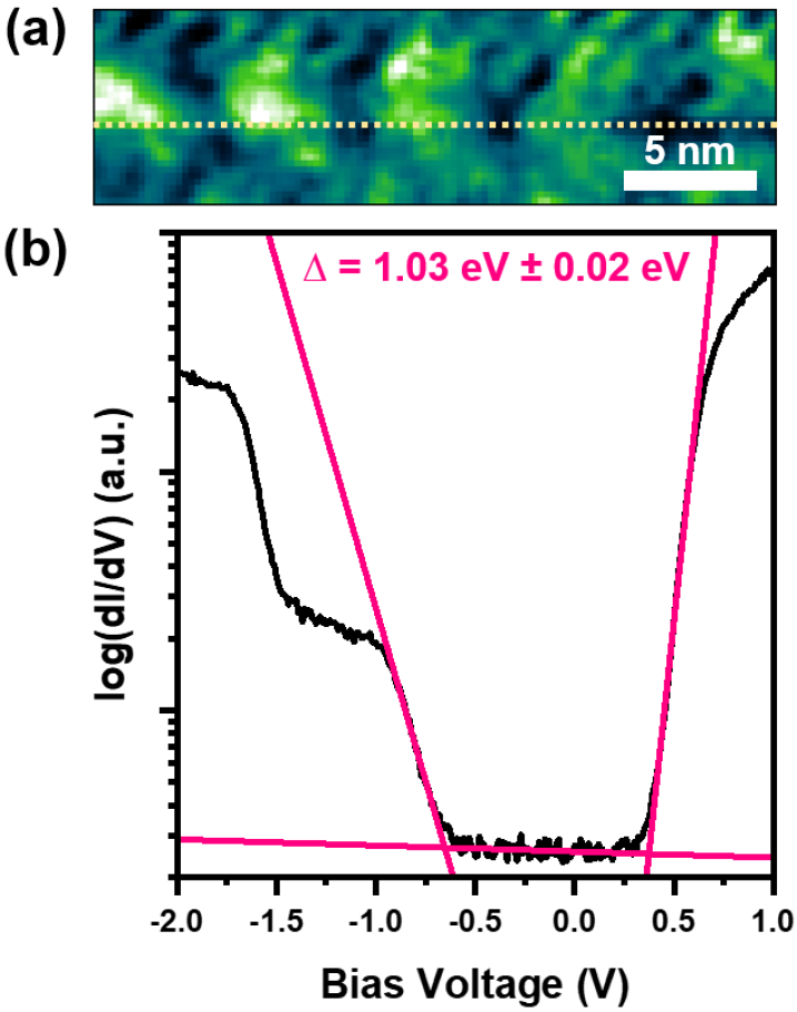
Section III: Spectroscopic gap calculated from the average spectra
