Switchable-magnetisation planar probe MFM sensor
Abstract
We present an alternative switching-magnetization magnetic force microscopy (SM-MFM) method using planar tip-on-chip probes. Unlike traditional needle-like tips, the planar probe approach integrates a microdevice near the tip apex with dedicated functionality. Its planar surface paves the way for freedom in ultra thin-film engineering and micro-/nano-tailoring for application-oriented tip functionalization. Here, we form a microscale current pathway near the tip end to control tip magnetisation. The chip like probe or planar probe, was applied to study the complex magnetic behaviour of epitaxial transition metal oxide perovskite LaMnO3, which was previously shown to behave as complex material with domains associated with superpara-, antiferro- and ferromagnetism. To this end we successfully imaged an inhomogeneous distribution of weak ferromagnetic islands with a resolution better than .
![[Uncaptioned image]](/html/2302.11387/assets/Figures/ToC.png)
For Table of Contents Only
Key words: AFM, MFM, tip design, weak magnetic, LMO3, metal oxide.
0.1 Introduction
Magnetic force microscopy (MFM) is a widespread method in fundamental surface studies and nanoscale technological applications with a high lateral resolution of up to tens of nanometers and force sensitivity1, 2. The working principle of MFM relies on the force interaction between the tip’s magnetic stray field and a samples’ spatially varying magnetic textures. By nanoscale utilization of this magnetic force interaction, MFM covers a wide operational range from characterization to manipulation of magnetic objects 3, 4, 5.
Despite its extensive use, a general MFM hits its capability limits mainly in lateral resolution of imaging materials with weak or time-varying magnetization. For instance, low coercive and weak ferromagnetic (FM) or superparamagnetic (SP) structures generally require an external magnetic field to saturate 6, and without this the magnetic force to the tip is weak or may be undetectable by the bandwidth of the MFM. Hence, nonmagnetic interactions such as those of electrostatic origin can mask the magnetic signal7, 8, 9. To obtain the pure magnetic signal of nanoscale weak FM or SP textures, such as isolated islands, an MFM variant called switching magnetization force microscopy (SM-FM) 10, 11 or controlled magnetization-MFM (CM-MFM) 8 stands out by extracting such signals out of the detected force 11, 12, 9. Beyond traditional MFM, SM-FM measures a relative force change due to controlled altering of the magnetic state of the tip or the sample (or both). Only the magnetic field interaction is sensitive to the relative magnetic polarities between the tip and sample and hence can thus be detected.
The need for a SM-FM imaging technique with a capability of imaging weak FM or SP islands with a resolution beyond can be found in the study of epitaxial complex oxide perovskites such as LaMnO3 (LMO3). Wang et al. 13 have shown that epitaxial LMO3 reveals an abrupt transition from an antiferromagnetic (AF) state to a ferromagnetic (FM) depending on the thickness of the LMO3 layer. The magnetic transition occurred at a film of atomic unit cell (u.c.) thickness. Furthermore, Anahory et al.14 observed inhomogeneously distributed SP islands besides the FM domains, with the former only detected following an applied in-plane magnetic field of variable strength. Both groups used a scanning SQUID microscope (SSM), albeit with different lateral resolution, to image the LMO3 sample’s stray field distribution. However, the SSM imaging performed by Anahory et al. 14 could not go beyond a resolution of , which left the SP island size to be only indirectly inferred between and .
To solve the problem of limited imaging resolution of traditional MFM, we carefully designed a new type of SM-FM sensor. To this end, we design a magnetic tip with a stray-field of several hundred mT strong enough to saturate the magnetic textures. The tip is realised by forming an oriented single domain state near the tip apex 15. Traditional needle-like MFM tips generally only generate up to a few tens of mT of stray field 16, 2. With this approach the LMO3 weak FM domains are simultaneously saturated and profiled for imaging by the same tip. The tip’s stray field decays rapidly from the tip and hence, by changing the height of the tip with respect to the sample surface the weak magnetic textures can be actively saturated.
We demonstrate that our sensor is capable of imaging magnetic textures of LMO3 with a resolution beyond . For this, we present a new approach combining planar chip-like probes17, 18, 19 with highly sensitive tuning fork force sensors which we call the switching-magnetization planar probe (SM-PP) and is illustrated in Figure 1a. This method aims to provide an on-chip reorientable tip magnetization with no required external magnetic field, to act as an switchable magnetic force sensor.
0.2 Results and Discussion
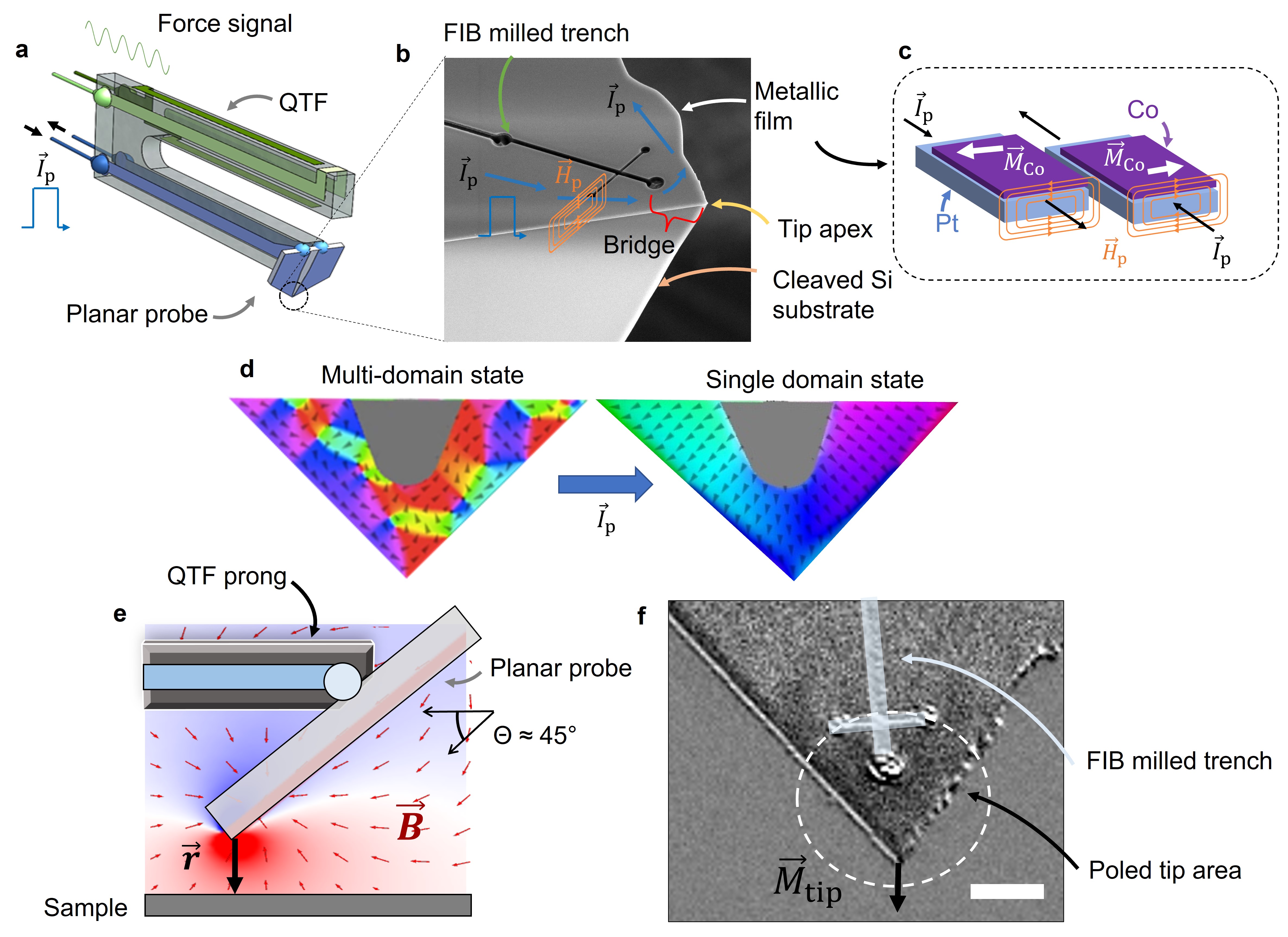
The working principle of the SM-PP relies on switching from a multi-domain state of the tip to a poled single domain via an internally generated Ørsted field () within a planar chip-like probe, as illustrated in Figures 1a, b and d. Initially, the magnetic layer on the tip is in a multi-domain state with a closed flux loop, Figure 1d. The direction of this flux may be irregular, and hence inappropriate for perturbing weak FM islands. The planar probe design used in this study has a bi-metallic structure of thin-film components: the current-carrying layer and the ferromagnetic layer, as depicted in Figures 1b and c. By sending an electrical pulse () through the current-carrying layer in a designated electrical pathway (called the bridge) near the tip apex, we generate an Ørsted field of controlled magnitude and well-defined direction which penetrates the ferromagnetic layer. This action leads to a singular domain state of the tip apex, with a preferable orientation.
The planar probe is formed by cleaving a silicon wafer into a small square piece with a tip apex 20, 17. Near the tip apex, i.e. the cleaved corner, naturally increases the flux density, increasing the tip stray field compared to a needle-like MFM tip. This magnetic field strength and distribution is discussed later on. The single domain state of the tip can be used to probe weak FM domains. To this end, we used a Pt film for the current-carrying layer and a Co film for the ferromagnetic layer, placed on top of the planar probe. Detailed fabrication procedures of the film and planar probe are given in Supplementary S1.
Contrary to the traditional passive needle-like MFM tips, we can orient the SM-PP multi-domains into a singular domain by only a single current pulse as often as needed to combat transient tip demagnetisation, a known issue in MFM. The resulting tip domain after sending a current pulse is illustrated in Figure 1d. As a result, we can obtain consistently oriented tip domains, resulting in a predictable stray field in the tip vicinity, as indicated by in Figure 1e. Figure 1e illustrates the side view of the SM-PP with the tip stray field distribution predominately out-of-plane from the sample’s perspective. In Supplementary S4 we discuss in-depth the tip stray field distribution derived from a numerical study. Finally, Figure 1f shows a Kerr microscopy image of the SM-PP, after having sent a current pulse of sufficient amplitude. A poled tip domain is formed as observed with the dark contrast near the apex, highlighted within the dashed circle.
We attached this functionalized planar probe to a mass retuned 20 quartz tuning fork (QTF) force sensor with integrated electrical access to the probe for the current pulse , as schematically illustrated in Figure 1a. QTF’s have been successfully used before for MFM 21 and are easily integrated in an UHV scanning probe microscope. The retuned tuning fork approach significantly improved the load capacity of the QTF sensor. As widespread AFM and MFM applications have previously experienced, once the mass exceeds several tens of 22, which is far below the mass of a chip-like probe, the oscillation’s Q-factor value drops to only several hundred from the original 40 thousand. This reduction in Q-factor results in a large loss in force sensing capabilities 23, 20. For degraded Q-factor sensors, we would be unable to use the planar probe for imaging magnetic fields of LMO3. To this end, the retuned tuning fork approach compensates for the mass unbalancing from planar probe attachment and recovers sensitivity. As a result we are able to restore the Q-factor to over at room temperature in ultra-high vacuum (UHV) 18, 20. In Supplementary S3 we discuss further the need for a high .
As a consequence, the Q-factor drops to only a few hundred 18, leading to degraded force sensing capabilities. The same effect can arise from the additional wires connecting the current control signal for pulsing, which is the reason why dedicated electrical contacts to the tip are now integrated on the tuning fork itself 24. We solve the mass-imbalance by mass retuning 23 the QTF as described in our previous work 20 and utilising readily available electrodes on the tuning fork.
For extracting the magnetic signal of weak FM islands, the SM-PP needs to change to a fully oriented near the tip apex, starting from a multi-domain state. We turned to finite element modeling (FEM), with COMSOL™, to simulate the generated Ørsted field within the bridge to assess the required magnitude for tip magnetisation control. Furthermore, we can investigate the thermal response of the tip by Joule heating.
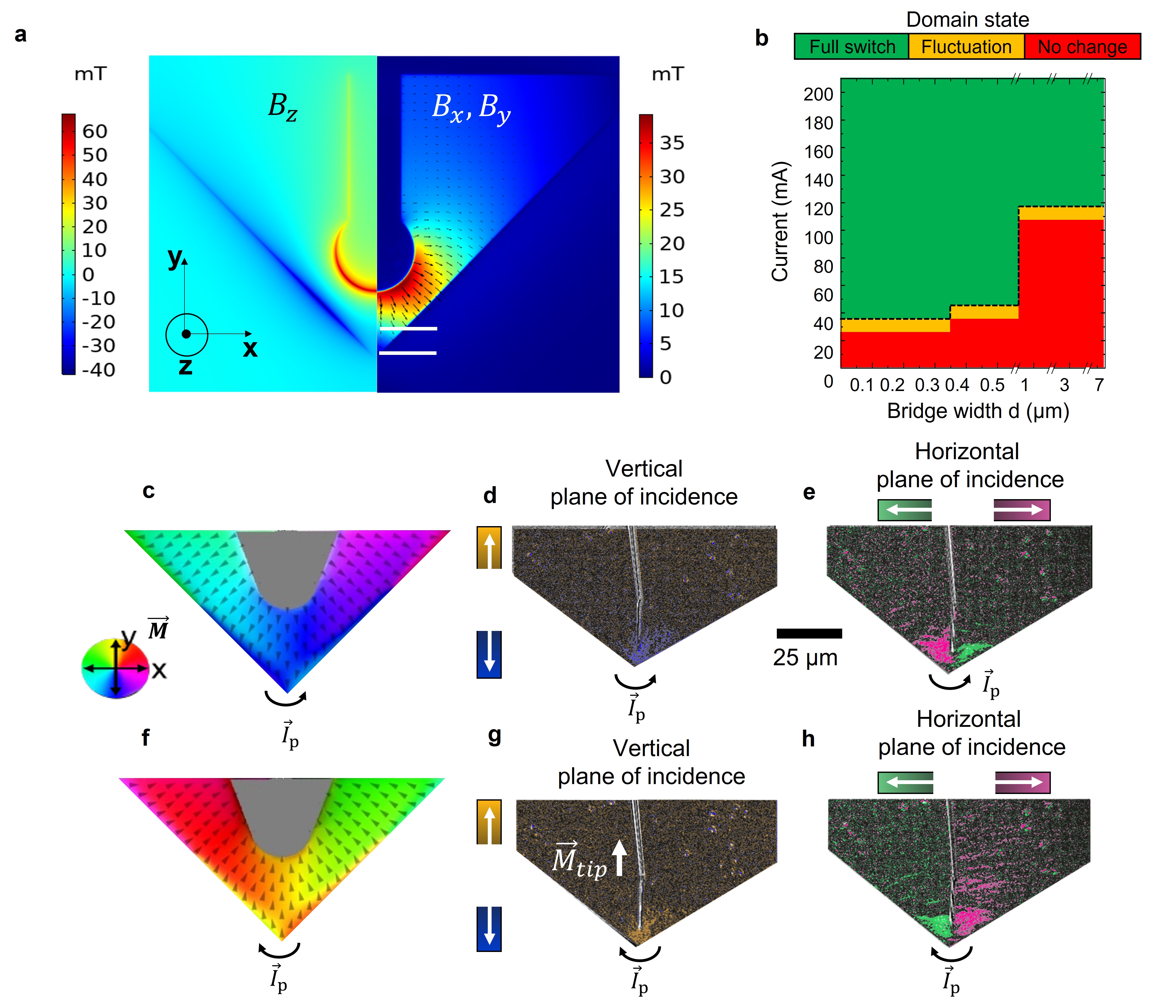
Figure 2 presents the numerical and experimental validation of the magnetic switch of SM-PP tip. The simulations cover various bridge widths in the range from to and different values from to . The pulse duration is . See Supplementary S4 for details on the simulations. First, Figure 2a shows the calculated spatial field components of of a bridge under application of . The in-plane field components and of follow the bridge structure. This indicates that both symmetric sides of the tip have opposing magnetic direction, as is evident from the current flow pathway. Near the tip apex, and are relatively small since the current density is lowest (between the white lines of Figure 2a). A strong out-of-plane component (Figure 2a) is only observed at the boundary of the tip and bridge, but is of little importance with respect to the in-plane magnetisation of the Co film. At just away from the tip apex, above the upper white line, the in-plane magnetic field is larger than which implies the nucleation of oriented in-plane Co domains. In Supplementary S1 the magnetisation response of the Co film is given.
Following, is used as an input parameter within Mumax3 to calculate the magnetisation response (switch vs. no switch) of the Co film at the tip apex, as a function of the bridge width and . In Figure 2b the color scale represents three different states of the tip magnetization after applying . Green means the tip end domain shows a 180° reversal, so a full switch. Yellow represents an observed modification or a limited rotation by less than 180° in the tip domain. Red implies that the magnetization remained identical to the pre-pulse orientation. The results show a few tens of mA increase in critical current level for the bridge gap width values from until , as given in Figure 2a. For the bridge gap widths greater than , the critical current shows a larger increase.
Although the nanometer scale of the bridge can be achieved with various techniques and types of lithography, in our experiments we used focused ion beam (FIB) milling. This resulted in bridges on the micrometer scale and as the simulations results shows, we require a current magnitude in the order of . Supplementary S1 discusses the FIB fabrication in further detail. When we simulate a current pulse with amplitude and duration for a bridge of , the tip magnetization changes fully accordingly to the pulse polarity, as shown in Figures 2c and f. The notion of tip switch at values below is important, especially for micrometer scale bridges, because it significantly limits the Joule heating, as we discuss later.
Based on the simulation results, a Kerr microscopy experiment was performed to validate the magnetic switch. The Kerr microscopy experimental details are given in Supplementary S2. Gray/black tones in Figure 2d, e, g, and h represent Co domains preserving initial orientations before the pulse, upon applying a current pulse. False colored areas represent the Co domains’ response to . Figures 2c and f indicate the orientation in the vertical direction expressed by the blue-to-yellow color scale. Figures 2d and g show the domain orientation in the horizontal direction, given by the pink-to-green color scale. The domain is mainly confined to the bridge region, as only here the current density is sufficient for inducing Co domain reversal. Along the length of the FIB bridge, the domains are inverted (pink and green), which follows closely those of the numerical simulations of Figures 2c and f, validating the realisation of the SM-PP.
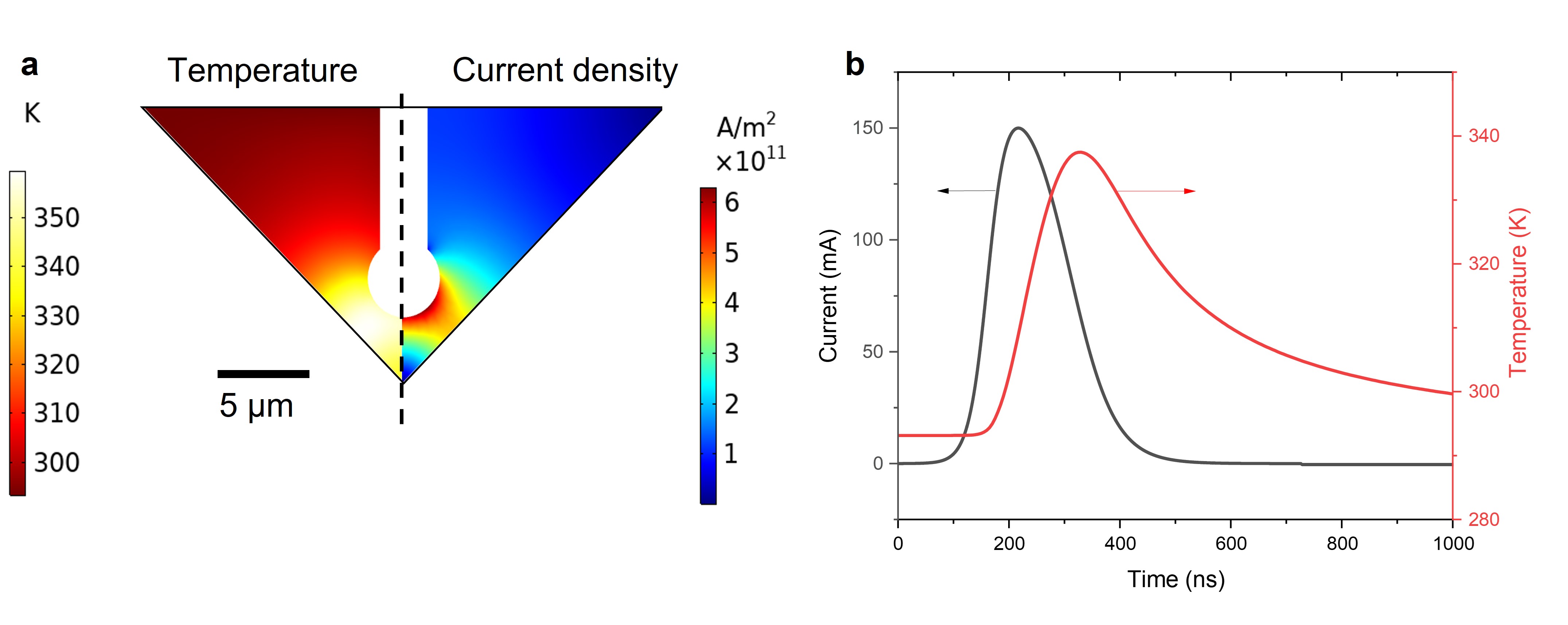
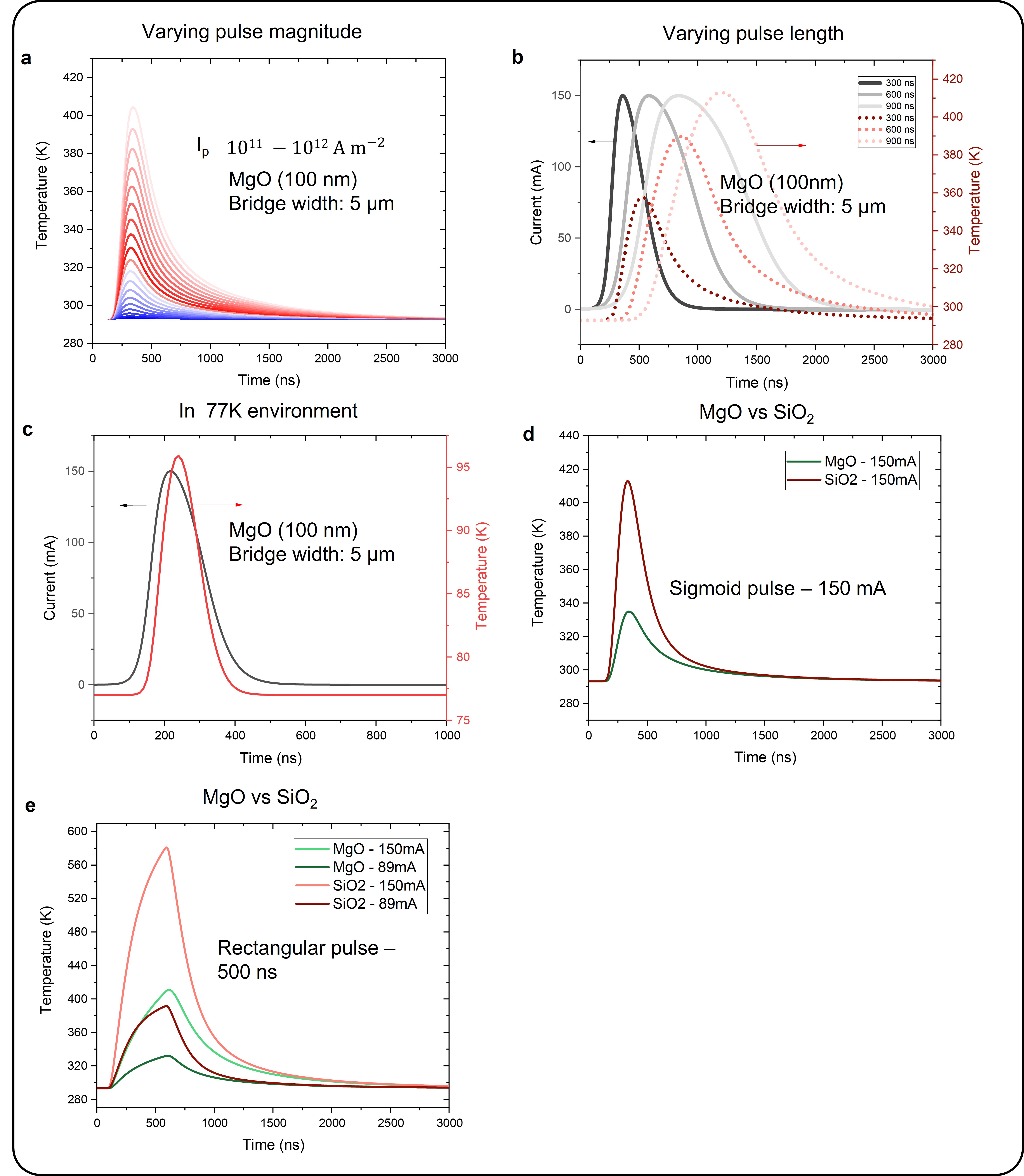
After applying , the temperature increase should be excessive i.e. above , because it would hamper operation in UHV and degrade the tip’s metallic layers. Examples and solution by metallic layer composition with respect to preventing degradation of tips are discussed in Supplementary S1. Hence, we modelled the (transient) temperature response of the tip for for an upper limit of thermal increase. Figure 3a compares the simulated spatial current density across the bridge for a of , with the thermal profile. As expected, the current density is highest near the shortest width of the metallic film and is in the order of . Yet, the maximum temperature increase is observed to be only , which means operation in UHV is possible and would minimize Joule heating damage to the metallic films. We experimentally pulsed several tips for tens of times and no degradation was observed. The transient heating response was also simulated, with the results given in Figure 3b. Here, a asymmetric double sigmoidal pulse, see Supplementary S4 for pulse details, is simulated. The temperature decreases quickly within a microsecond due to efficient thermal dissipation of the Si substrate. We studied the effects of substrate capping material, i.e. Si coated with SiO2 or MgO, on this thermal dissipation and the results are also discussed in Supplementary S4.
To conclude the first part of this work; the design, fabrication and optimisation of SM-PP provides us a SM-PP sensor with high Q-factor. Combined with the current-controlled tip magnetization it enables the possibility to study the magnetic surface textures of LMO3 13, 14. For the second part of this work we turn to applying the SM-PP sensor to saturate and image the weak FM islands, aswell the AF domains the former are embedded into, of epitaxial LMO3.
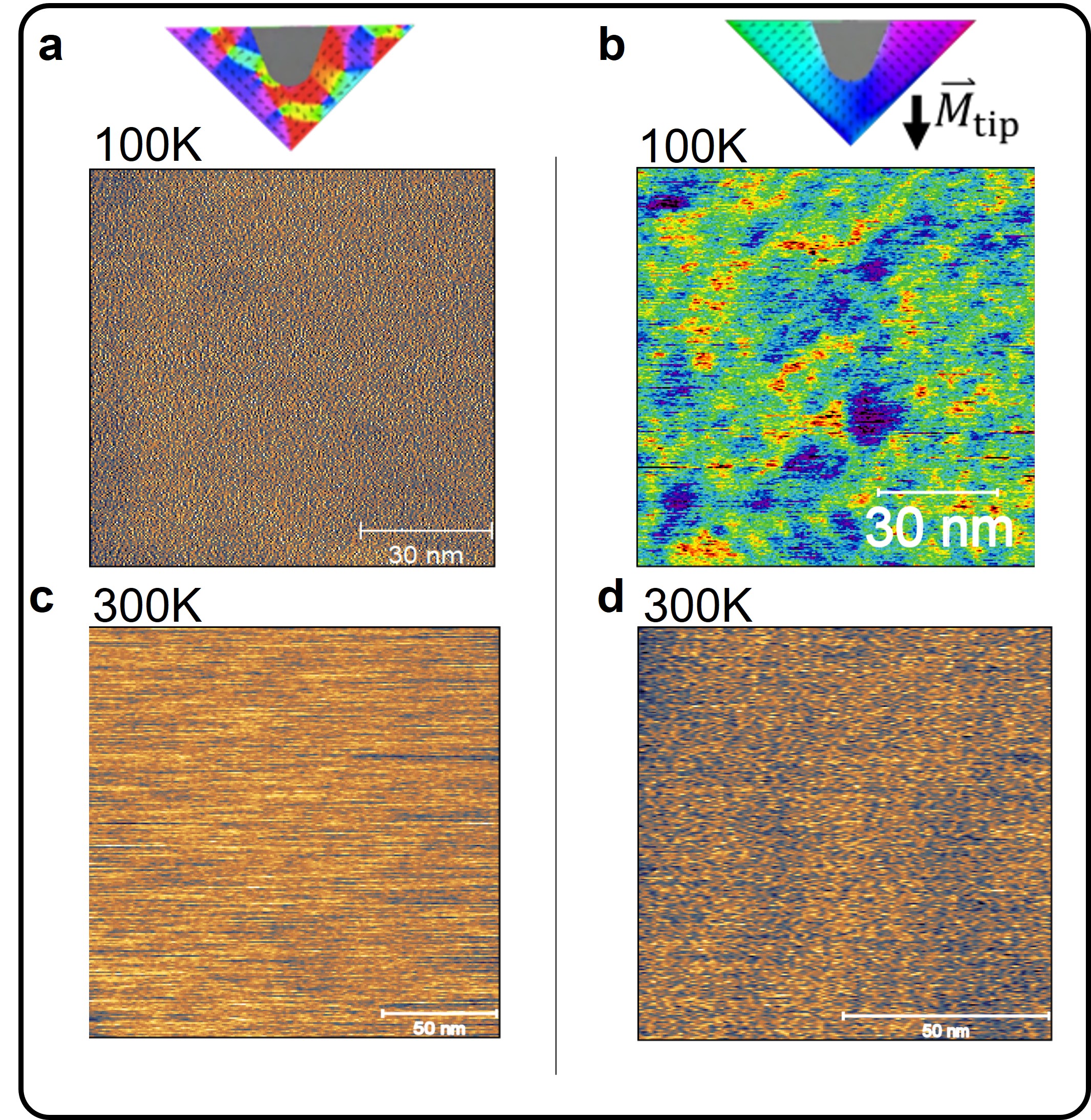
The magnetic texture of a 6 u.c. LMO3 on STO3 sample was imaged with our MFM operating both below ( ) and above ( ) of LMO3’s 13. The first aim was to identify the AF and weak-FM texture distribution across the surface. Secondly, the SM-PP is able to magnetize magnetic islands by the tip’s oriented stray field exceeding , see Supplementary S4, and hence the size of the magnetic islands can be observed with a lateral scale between and 14. The same SM-PP sensor was used for all imaging, with Frequency Modulation (FM) feedback. The scanning parameters are kept constant throughout all the measurements, see Supplementary S6 for methods and experimental details.
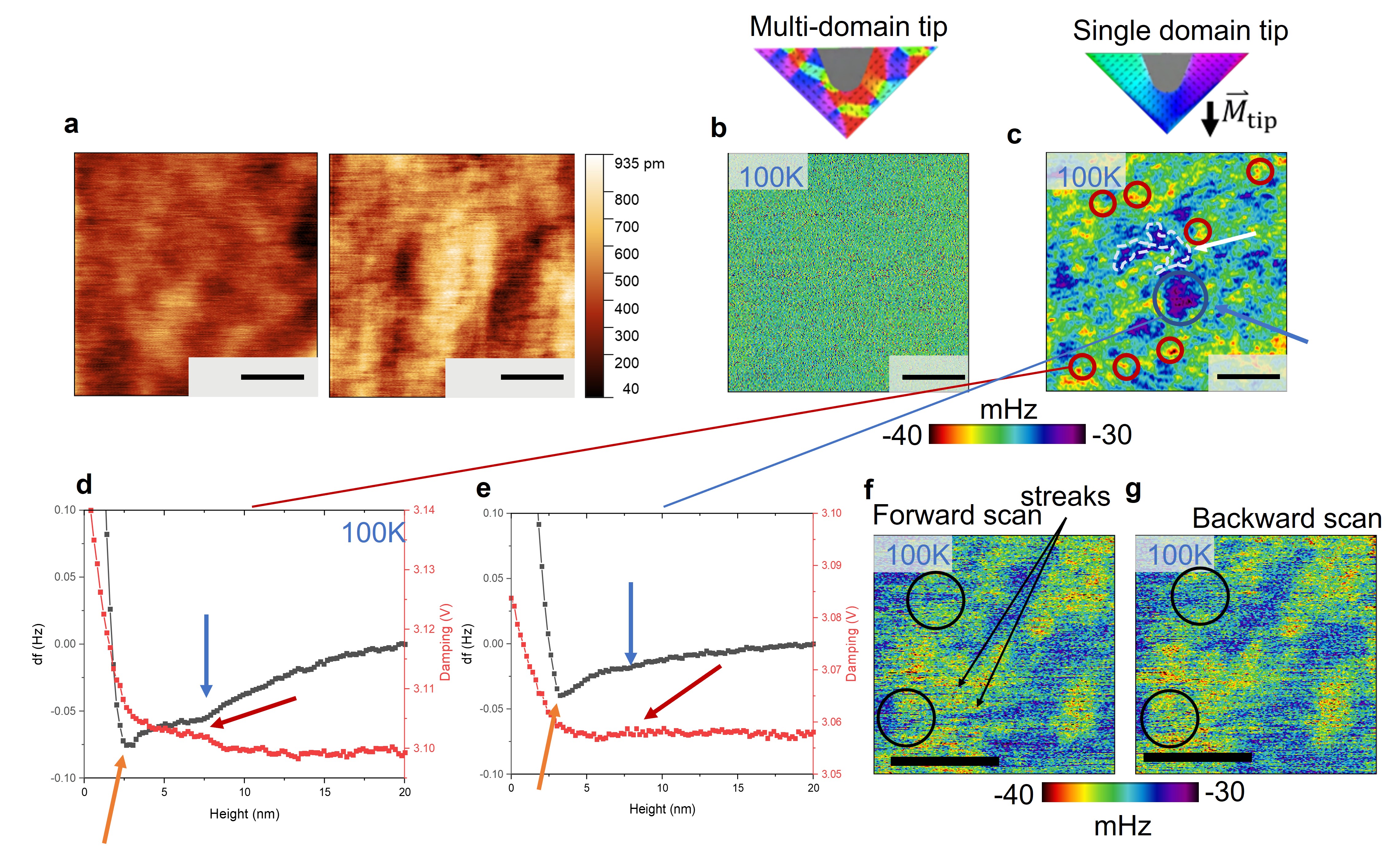
First, we scanned at a temperature of and imaged a plateau of the LMO3/STO3 stepped surface. The 9090 topography images are given in Figure 4a and demonstrates a LMO film RMS roughness of . Although the surface of LMO3 can show up to 1 u.c. roughness variations, in-homogeneously distributed across the stepped surface, which is a known surface feature for manganites 25. The lateral resolution in topography is limited by the relatively large amplitude of used for detecting the long range magnetic force. Ideally, one would use a small amplitude for high resolution topography and a large amplitude for lift mode magnetic imaging 21. We leave this for future work, as currently this approach of consecutively switching of the amplitude introduced large drift in our setup.
After obtaining the local topography, we switched to MFM. The MFM signal was first acquired with a multi-domain, closed flux tip, where negligible (out-of-plane oriented) stray field should interact with the sample magnetic domains. Indeed, Figure 4b shows that no MFM signal could be measured below the noise level of . The lack of topography cross-talk in the lift mode image also demonstrates that the lateral variation of the electrostatic force is neglible.
Following, the tip was pulsed by a current pulse for , which aligned the tip domain in the downward position, as indicated schematically in Figure 4c and confirmed with Kerr microscopy prior. For safety, the tip was retracted by from the surface during the pulse, which can give rise to lateral drift of around in our SPM at these temperatures. With the magnetically oriented tip, we continue MFM imaging at and observed a complex landscape of magnetic textures across the scanned area, as given in Figure 4c. The smallest magnetic objects are highlighted with red circles in Figure 4c, which also correspond to the strongest attractive magnetic forces. These features have on average a diameter of . We attribute these area’s as stray field induced magnetised domains. Observing the nominal size, it is very likely that these corresponds to the weak FM textures 14, even at .
Performing force-distance (F-z) spectroscopy on the red islands of Figure 4d showed complex behaviour and provides more evidence for weak FM properties. The tip was retracted up to above the surface, and then lowered until a notable repulsive fore was observed. The frequency shift was measured during spectroscopy. Evidence of the tip stray field induced magnetic alignment is given in Figure 4d. We observe four distinct regimes; firstly we note a long-range attractive forces between and . This can be assigned to long range electrostatic forces. At around , a sudden negative change in frequency (force) is observed as indicated with a blue arrow. We attribute this to the significant increase of the magnetic field the sample experiences as the SM-PP tip approaches the weak FM domain and hence saturating it. At , indicated with an orange arrow, the attractive van der Waals force region is noted. At very small tip-sample distances the frequency shift becomes positive evidence of repulsive forces. We also measured the damping, a sign of energy loss via local magnetization change of the weak FM islands 7. In Figure 4d, the red curve shows a sudden rise in the damping as indicated with the red arrow. Likely, at this distance the weak FM islands are magnetized periodically as the tip oscillates up and down. As a comparison, Figure 4e shows the same F-z spectroscopy experiment performed on the blue areas of Figure 4c. Less perturbing of the attractive force is noted, and no measurable dissipation change is observed as highlighted with the colored arrows. We conjecture that those blue colored areas are the antiferromagnetic domains.
Generally, the weak FM features (coloured red) are embedded in magnetic labyrinth-like domains colored yellow/green in Figure 4c. These domains are continuous and spread across the surface. Furthermore, they have smaller attractive force than the weak FM areas. Due to the tip’s large stray field induced magnetization of LMO3, no repulsive area’s could be observed. Areas depicted in blue are observed in two distinct regimes. First, we note distributed areas highlighted with the dashed white line. Secondly, blue circular like objects are noted as highlighted with the blue circle. These objects show very little attractive frequency shift. Hence, excluding electrostatic forces as these are constant across the surface, these domains form an antiferromagnetic texture, corroborating the SSM observations of Wang et al. 13 and Anahory et al. 14.
Furthermore, we note that the tip stray field can induce local magnetic perturbations in the real-space imaging. By comparing the forward and the backward scan, Figures 4f-g, the areas highlighted in the black circle show clear distinction between the two images. We conjecture that the field from the tip perturbed the local weak FM domains. This would also be in agreement with the observation of streak-lines as indicated with the arrows.
In conclusion, the results lay strong indications of the imaging capabilities of the magnetically controllable SM-PP tips for weak FM islands with a resolution higher than . Firstly, we achieved a repeatable control over the magnetization at the SM-PP tip with a consistently distributed domain state at the tip apex. Following, we demonstrated imaging of a complex magnetic texture of the rare-earth metal oxide perovskite LMO3 with nanometric identification of weak FM islands. For further investigation of LMO3 the SM-PP can be employed for ultra-high resolution imaging of the local u.c. variation in film thickness and the possible correlation with weak FM islands. Furthermore, the integration of the SM-PP in a LHe cryostat would increase the Q-factor by another order of magnitude, significantly improving the signal-to-noise ratio. Finally, future application the SM-PP can be combined with scanning tunneling microscopy functionality because of the tip metallic layers and electrode accessibility of the tuning fork. This way we can combine ultra-high lateral resolution imaging of conductive metal-oxide-perovskites and measure the long range MFM forces without the need to switch to different setups. This possibility opens up a approach to disentangle the atomic scale structure and long range magnetic ordering relations of transition metal oxides for application in spintronic and catalytic devices. Considering its enhanced sensitivity, the widened scope of tip-on-chip design can convert the MFM/AFM from a surface analysis tool with passive probes to a more sophisticated device with active more complex probes for characterization, e.g. nitrogen-vacancy centers diamond tips as quantum sensors for detecting ultra-small magnetic fields 26, 27 or currents 28.
0.3 Materials and Methods
0.3.1 Planar probe fabrication
The metallic layers was sputtered on a thin thin Si wafer (intrinsic, UniversityWafer). The wafer was cleaved by a diamond scriber in pieces and inspected by an optical microscope. Following, the tip apex radius was inspected and selected for a radius below by a ZEISS-Sigma SEM. A FEI Nova600i SEM-FIB was used to fabricate the bridge structure by Ga-ion etching. A sequential beam current of , and was used. Near the bridge the smallest current prevents damage and increases the etching resolution. The acceleration voltage was . The planar probe was placed onto the QTF (AB38T) prong with UV-curable resin with minimal volume (less than ) employed by the use of a syringe needle. Silver paste was used to connect the electrical leads of the planar probe to those of the QTF. EPO-TEK 4410 was used to connect the wires from the QTF to a custom PEEK sensor holder. Detailed fabrication procedure is further outlined in Supplementary S1.
0.3.2 Kerr Microscopy
A Zeiss Axio Imager.D2m Kerr microscope was used with a magnification lens, assembled by Evico Magnetics with a polariser/analyser pair and manual slit diaphragm. The setup was combined with a set of water cooled Helmholtz coils for magnetic moment alignment by in-plane magnetic fields with respect to the Co film orientation. Kerrlab software was used for data acquisition.
0.3.3 Numerical calculations
MuMax3 was employed to simulate the domain structure of a Co film. Exchange length of and grid unit cell of 4x4 were used. For study of the thermal and magnetic properties of the SM-PP COMSOL Multiphysics was used with the AC/DC module and Heat Transfer module. Further numerical details are outlined in Supplementary S4.
0.3.4 Imaging in UHV
A Scienta Omicron VT-SPM setup was modified to carry two additional electrical contacts for pulsing the planar probe tip. The contacts are constructed from 2 gold coated pogo pins placed on a custom PEEK holder onto the scanning tube. An square wave generator (Agilent 33120A) was connected to a custom MOSFET circuit to reduce the pulse down to several hundred ns. Coax cables where used to connect the function generator to the VT-SPM. Detailed imaging methods are outlined in Supplementary S5.
The authors thank W. Dijkstra for assistance in both the modification of the UHV-SPM and fabrication of the custom pulse generator. Special thanks to H. Hilgenkamp of Twente University of Technology, Netherlands, for providing the 6 u.c. LaMnO3 thin film on SrTiO3 sample. O. Kurnosikov acknowledge support from ANR-15-IDEX-04-LUE CAP-MAT ans by the “FEDER-FSE Lorraine et Massif Vosges 2014–2020. Financial support from the Eindhoven University of Technology is acknowledged.
0.4 Supplementary S1: Fabrication and characterisation of the SM-PP
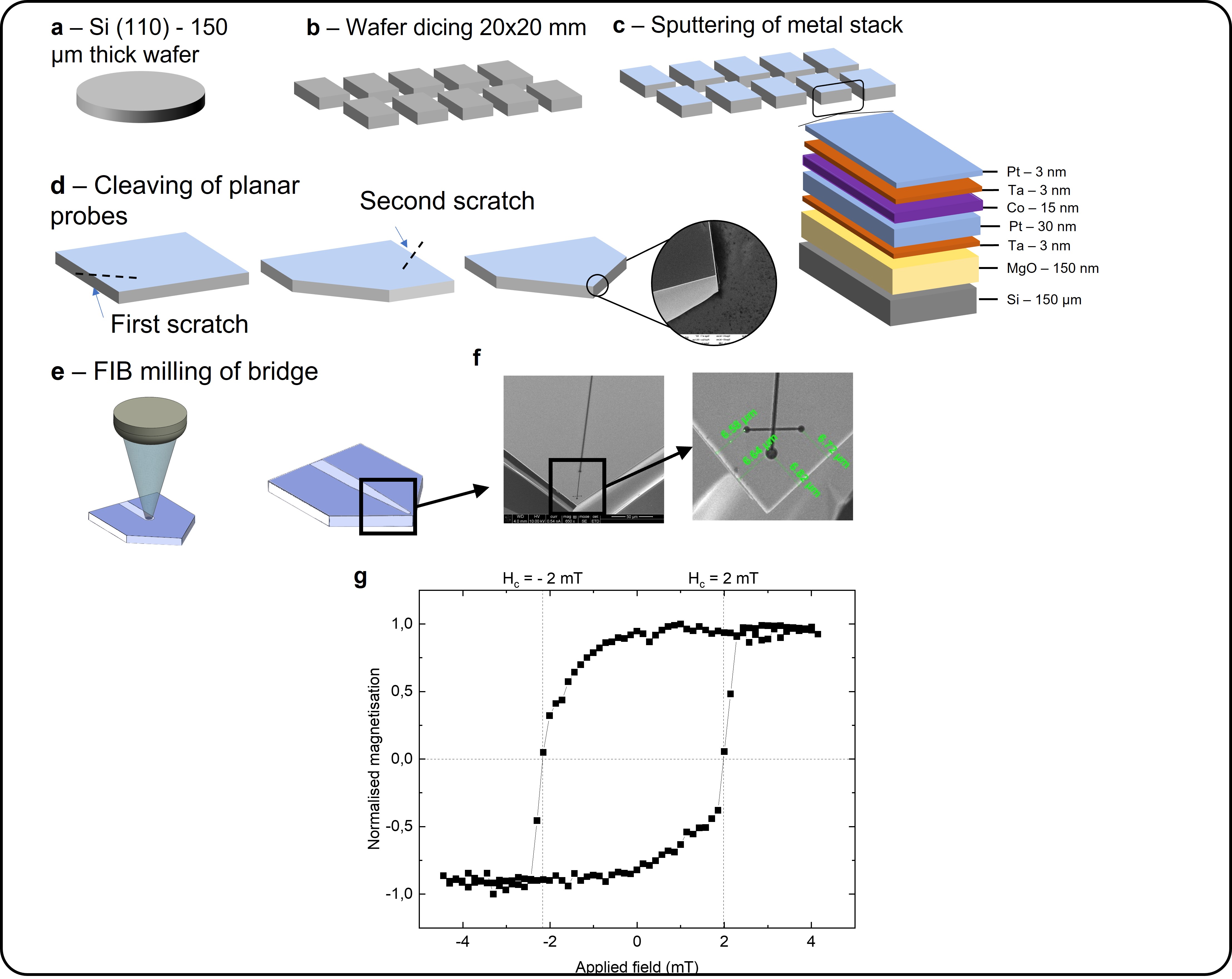
The fabrication procedure of the SM-PP is schematically given in Figure 5. The use of a thin Si wafer (intrinsic, from UniversityWafer) makes it possible to facilitate easy mechanical cleaving without having to apply large mechanical force and simultaneously reduce the planar probe’s mass. First the wafer is diced into x pieces, as shown in Figure 5b. Single crystal silicon (100) is known to cleave in atomically smooth planes 29. By cleaving in two perpendicular directions a nanometer scale tip apex can be achieved. The cleaving results in square pieces up to x, with the tip apex’ are evaluated for their radius (sharpness) with SEM, see Figure 5e for a large scale image. For integration into a sensor, tips with a radius below were chosen for further fabrication steps, tips with larger radii where discarded. Because of the square nature of the cleaved planar probes, each piece offers up to adequate tip apices. This makes the availability of many excellent tips with a small radius very likely, fabricated in a short amount of time.
With FIB milling, significant Ga-ion implantation occurred into the Si wafer which shortened the milled trench and voiding the bridge functionality. Hence, we resorted to growing an insulator spacer layer of SiO2 or MgO between the metallic stack and the wafer. The integration of a microscale current pathway requires to reduce thermal-induced damage by excessive Joule heating. To enhance thermal management near the tip apex a high thermal conductivity MgO spacer layer is sputtered on top of the silicon wafer. MgO has a sufficient thermal conductivity of about 30. Furthermore, MgO simultaneously facilitates electrical insulation to reduce electrical leakage currents. In Supplementary S4 we discuss the thermal dissipation behaviour between Si/MgO and Si/SiO2 substrates after sending a current pulse through the bridge.
Next, the metallic multilayer was deposited. The planar probe metallic layer consists of the following structure, see Figure 5c. First, a tantalum (Ta) seed layer is grown to induce good mechanical adhesion of the subsequent metal layers with the MgO/Si substrate. The Ta seed layer also smooths the surface roughness of the MgO layer to to some extent, which still results in a final RMS roughness of . Such a reduced roughness can actually be beneficial as it can be expected that near the cleaved tip apex small nanometer scale bumps form the nano-tip and reduce the van der Waals forces compared to a fully triangular structure, as it scales with the tip volume. The measured roughness of SiO2 and MgO layered films are given in Figure 6.
Subsequently, a current-carrying Pt layer is grown. This relatively thick Pt layer has the lowest film electrical resistance of the metallic stack; the majority of the current will flow through this layer. The ferromagnetic film is made from Co. Finally, the stacking is capped with of Ta and of Pt to induce high mechanical rigidity of the tip apex and prevent native oxidation.
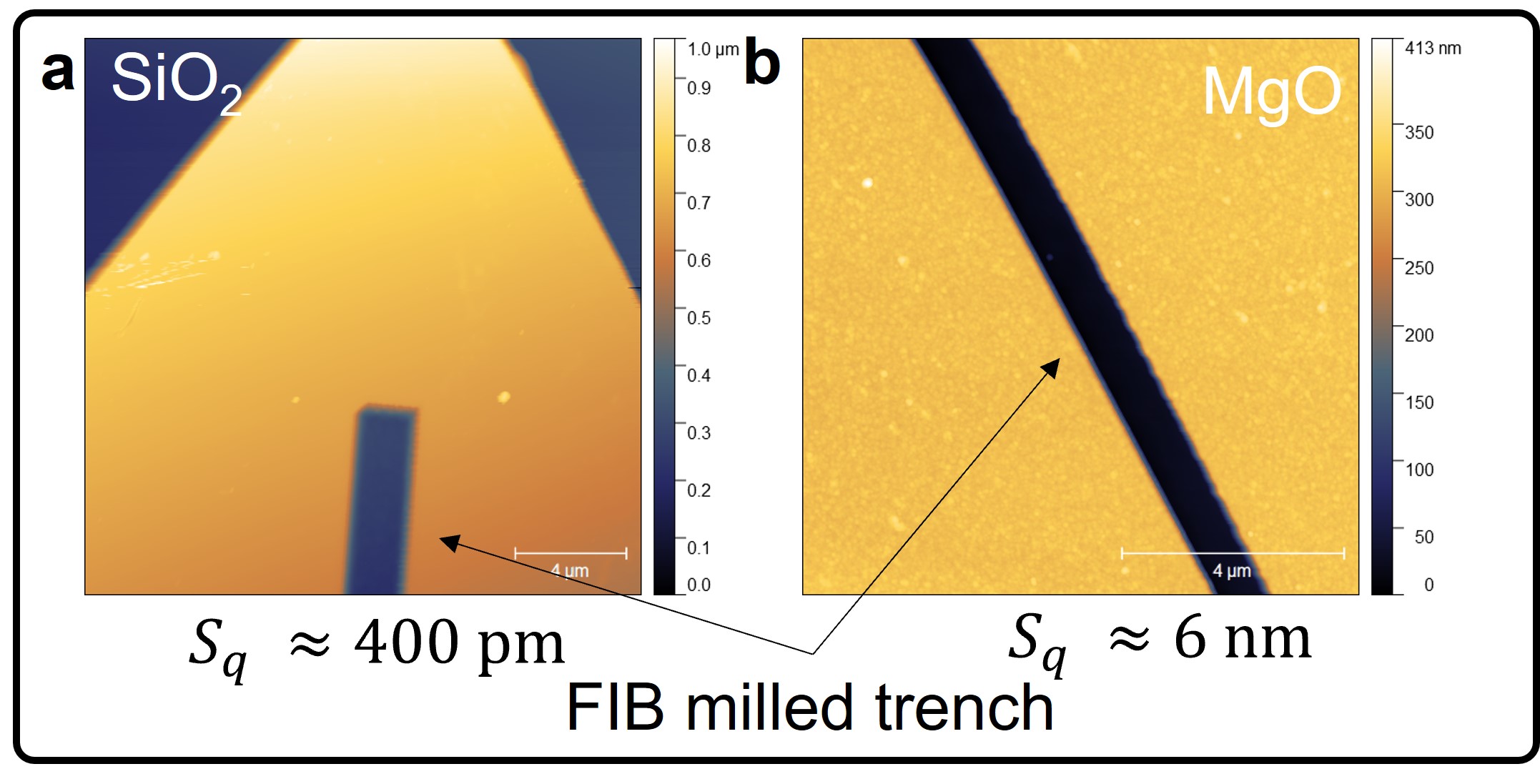
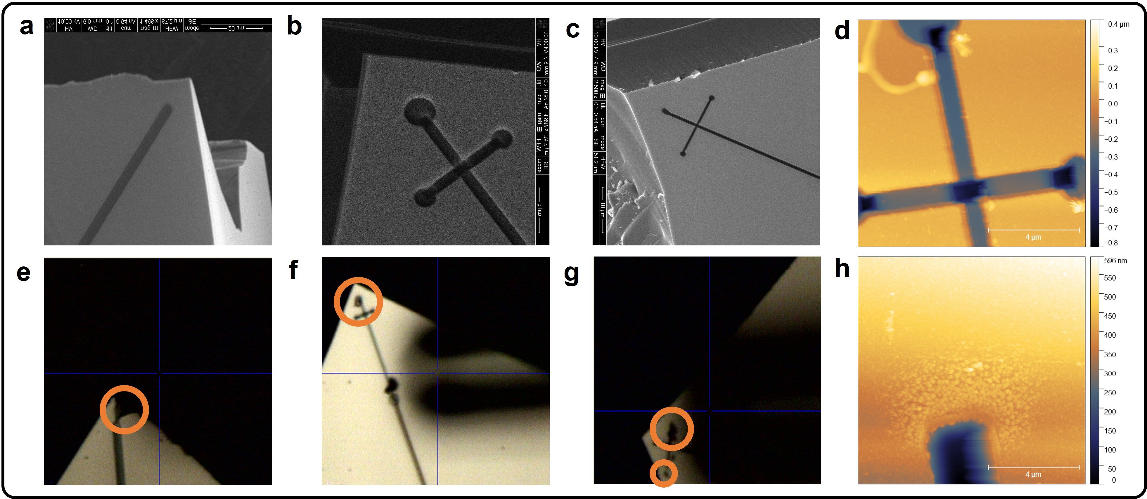
When using (native) SiO2 as a spacer layer between the intrinsic silicon substrate and the metallic stack of the planar probe, the low thermal conductivity of SiO2 of only , limits the thermal durability of the device. This low thermal conductivity was found to be insufficient to prevent damage from Joule heating to the bridge when using pulses above . Limiting the current below proved insufficient for full domain reversal for many devices with bridges in the micrometer widths. Figures 7a, b and c show SEM images of FIB fabricated tips with either a single straight trench or the crossed configuration. The tips have a nominal bridge width, measured from the end of the trench to the tip end, of (a) , (b) and (c) . Figures 7e, f and g show optical microscope images of observed tip damage, highlighted with orange circles, after sequential pulsing. In these images, the metallic films have clearly degraded by excessive Joule heating. The Joule heating is most intense where the bridge width is smallest i.e. near the tip end, corresponding to the highest current density. Figures 7d and 7h show AFM topographic images of the FIB trench end, after 2 pulses. Clearly, the metallic film shows first signs of degradation or ”peel-back”, before full layer destruction occurs. With the inclusion of MgO, which is directly sputtered on top of the silicon wafer, we observed no Joule heating induced damage. MgO has a much high thermal conductivity of 30. MgO devices pulsed over 25 times showed no degradation or change of the bridge resistance, even for pulses up to .
0.5 Supplementary S2: Kerr microscopy
A Zeiss Axio Imager.D2m Kerr microscope was used with a magnification lens, assembled by Evico Magnetics with a polariser/analyser pair and manual slit diaphragm. The setup was combined with a set of water cooled Helmholtz coils for magnetic moment alignment by in-plane magnetic fields with respect to the Co film orientation. Kerrlab software was used for data acquisition. The slit diaphragm makes it possible to filter light and select a magnetisation direction to visualise (horizontal or vertical) moment sensitivity. A custom-made sample holder was fabricated with integrated electrical wiring. The holder offered 3-degree’s of positioning freedom needed for positioning of the SM-PP below the Kerr lens. A custom pulsing circuit was used to pulse a to current for to . By ramping up the current in consecutive pulses, the domain switching threshold was found.
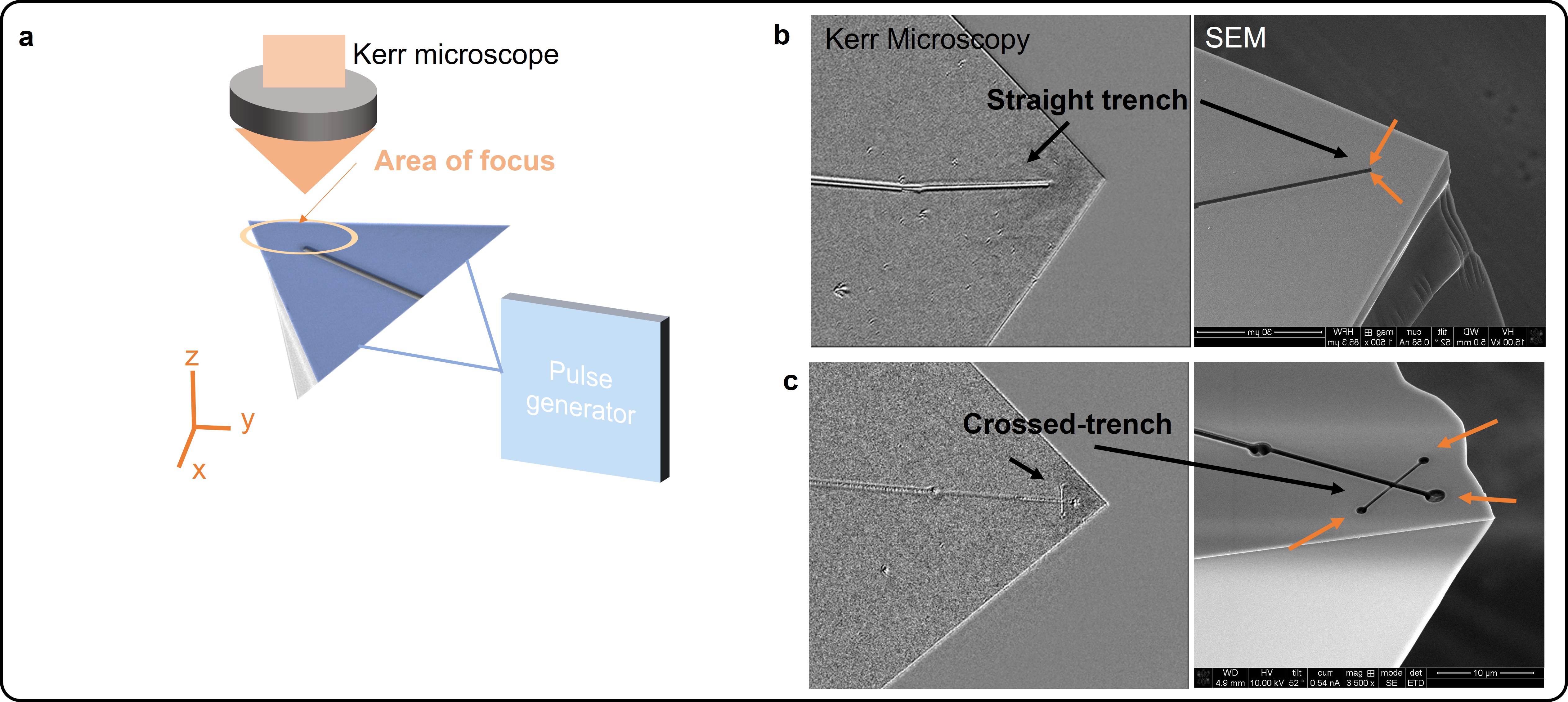
It was found that fabricating a single straight FIB trench does not always result in a stable magnetic domain reversal, with an example given in Supplementary Figure 8b. For these straight trench devices, a stable domain was observed only after several consecutive current pulses. Even then, the domain does not extend across the complete bridge region, as indicated with the black arrows. With a single trench structure, only two nucleation sites are formed, near the very tip apex where the current density is highest (orange arrows). Although our numerical model suggests that it is possible to fully switch the domain with a single pulse, we attribute some devices needing more pulses to the fact that the FIB bridge was not always placed perfectly placed along the mirror-symmetrical axis of the probe. Hence, the current distribution is not equal along the bridge which could hamper full domain reversal near the tip apex. In our numerical models we have always assumed fully symmetrical structures.
To remedy this problem a perpendicular and smaller trench was FIB milled near the original trench, close to the tip apex, see Figure 8c. This design adds an extra nucleation site, indicated with orange arrows, in close proximity to the bridge end. It was observed that this enables formation of a very stable domain that can be reliably reversed with a single pulse in all fabricated tips (number of tips exceeding 15). Figure 8c show gray-scale Kerr Microscope images focused on the crossed bridge design. Kerr sensitivity was selected which corresponds to the domain pointing in-plane. Thus, the double crossed trench solution overcomes the non-perfect mirror-symmetric alignment of the FIB trench and induces multiple nucleation sites across the bridge.
0.6 Supplementary S3: Note on the QTF function
The large mass of the planar probe would decrease the Q-factor below a few hundred, with strongly influencing the sensitivity of the force sensor 24. Hence, mass retuning of the QTF is performed by offsetting the mass of the planar probe carrying prong to equate that of the added mass of the oversized tip. This effectively restores to its pristine value 20. The need to enhance is vital by satisfying two requirements for the SM-PP to function. First, the frequency noise in frequency-modulation (FM) AFM scales inversely with 24. Hence, a higher results in larger signal-to-noise ratio needed to measure the smaller forces associated with magnetic stray field gradient sensing 24.
Second, due to the mentioned separation of the electrode layout, the actual force-to-voltage conversion signal by the piezo-electric effect of the quartz tuning fork, is measured in the upper prong of the QTF. This prong essentially measures the tip-sample force indirectly and works most efficiently if the two oscillating prongs operate in the anti-phase mode with little dissipation in the connecting node 20. A low would lead to insufficient coupling between the two oscillating prongs and hence impede operation of the force sensing. This is fundamentally different from the qPlus sensor, were only one prong oscillates and hence the force sensing is limited to this prong 24.
Using the retuned tuning fork approach, we explore the possibility of using a high spring constant () force sensors, which is remarkably higher than those of the qPlus (). With a high , the minimal detectable force gradient is reduced together with the detectable frequency shift down to several tens of mHz, according to the equation 24. Hence, the tip needs to scan only a few nanometers above the sample surface to measure the magnetic stray field gradients, above the noise level of approximately . This small simultaneously prevents the signals from areas beyond the dimensions of the tip to be picked up and hence the resolution can be increased significantly, needed for imaging nanometer scale SP islands of LMO3. Our SM-PP realises a above at room temperature, in ultra-high vacuum (UHV), which results in a noise floor of . For MFM imaging of nanometer sized SP textures, the high and large are beneficial, as forces coming from area’s not directly beneath the tip are not picked up by the SM-PP because the decreases rapidly below the noise floor.
0.7 Supplementary S4: Numerical calculations of thermal and magnetic properties
0.7.1 Influence of current pulse characteristics on Joule heating
The (transient) temperature response of the SM-PP bridge was numerically studied with COMSOL ™. First we address the current pulse shape.
In our SPM setup, capacitance of the cables that are connected to the SM-PP affect the pulse shape, resulting in a more asymmetric shape deviating from a square current pulse input. We simulate this curve in COMSOL using the asymmetric double sigmoidal function, which has the following functional form:
| (1) |
Here, defines the width of the pulse, and together define the asymmetry of the pulse, is the centre of the pulse and is proportional to the amplitude of the current pulse . We fit Eq 1 to the real pulse of which we obtain the full-width-at-half-maximum (FWHM), and pulse amplitude .
Heat transport in ultrahigh vacuum (UHV) conditions is modelled via COMSOL™heat conduction. Thermal dissipation occurs via conduction within the planar probe and via radiative emission. The environment is set at room temperature, as is the case for the Scienta Omicron VT-SPM lacking a cryostat. Only the sample is cooled. The radiative thermal dissipation is set by the surface emissivity . We used the values for the following materials that were used in the functionalised planar probe: , , and . The other metals, Ta and Co, are neglected.
First, we consider the maximum current through the bridge without overheating it. To this end, we varied the current density in the planar probe, which is related to the total current via , where is the thickness of the main platinum layer and is the width of the bridge gap (), respectively. The situation we consider is the asymmetric pulse from Equation 1 with a current peak of , which amounts to a current density of . We vary the current density from to , in steps of . The results are shown in Figure 9a, in which the temperature barely increases by for the smallest current densities, and increases by approximately in case of the highest current density.
To characterize the temperature increase with respect to the current pulse length, we simulate three current pulses with a different pulse duration: , and FWHM. The pulses are indicated in Figure 9b in dark solid lines. The resulting temperature evolution at the probe’s tip end is shown in Figure 9b in dotted red lines. Indeed, the temperature increases with the duration of the pulse. The temperature increases by about in case of a short pulse, up to an increase of over for the pulse. This large difference illustrates that the current pulse duration has a major impact on the temperature increase, so the current pulses need to be as short as possible in order to prevent overheating the probe.
We also investigated the thermal aspects of the planar probe when it is cooled down to liquid nitrogen temperature (). The values of the surface emissivity are set to the same values as at . The temperature evolution of the probe’s tip at is shown in Figure 9c. Evidently, the temperature of the probe increases by only , which would make operation in a cryostat possible.
Finally, we discuss the thermal characteristics of a SiO2 layer. As Supplementary S1 discussed, the inclusion of SiO2 as a spacer layer to reduce electrical shorting by FIB milling, turned out to negatively impact the thermal dissipation, eventually leading to bridge damage after several pulses above . Numerical calculations of MgO and SiO2 are shown in Figure 9d. These plots show a temperature increase when SiO2 is used, to a maximum above . These values were calculated with a pulse of equation 1, with a FWHM of . In the case of a MgO layer, the temperature increase is less than , supporting the experimentally observed stability of MgO as a spacer layer. For comparison, we have also used a block pulse of with a magnitude of with the thermal response shown in Figure 9e, with much higher temperature peaks observed, exceeding over . Hence, the peak value needs to be minimized to only a few ns to prevent damage to the tip, and a block pulse is not sufficient.
0.7.2 MuMax3 calculation of tip domain orientation
MuMax3 31 was used in which a Co film was simulated, with an exchange length of and grid unit cell of 4x4 . The following values are taken to simulate the cobalt; saturation magnetisation = , exchange constant = and the order uniaxial anisotropy constant of .
0.7.3 Note on the magnetic stray field computation
To study the magnetic properties of the SM-PP, specifically its tip magnetic field component distribution , and and the field magnitude, a 3D COMSOL™FEM model was made. The SM-PP is modelled as a ferromagnetic Co layer with a magnetization of . In the main text we showed the stray field of the SM-PP in the in-plane direction of the tip as it extends outwards, when placed a certain height above a flat sample. In the calculations, the SM-PP and sample are placed in an air medium. Figure 10 presents the modeled stray field results.
Figures 10a and b show the field distribution at two different cross-sections: in the -plane, and parallel to the probe surface, respectively. Important to note is that the probe length is much larger than the tip-sample distance . However, for computational reasons the probe was made smaller (”cut-off”), which gives rise to an additional curvature of the field near the upper side of the probe. Near the tip, where the calculations were performed, the effect of this curvature has been taken into account during the final calculations. Figure 10c presents the calculated , and between the tip sample distance .
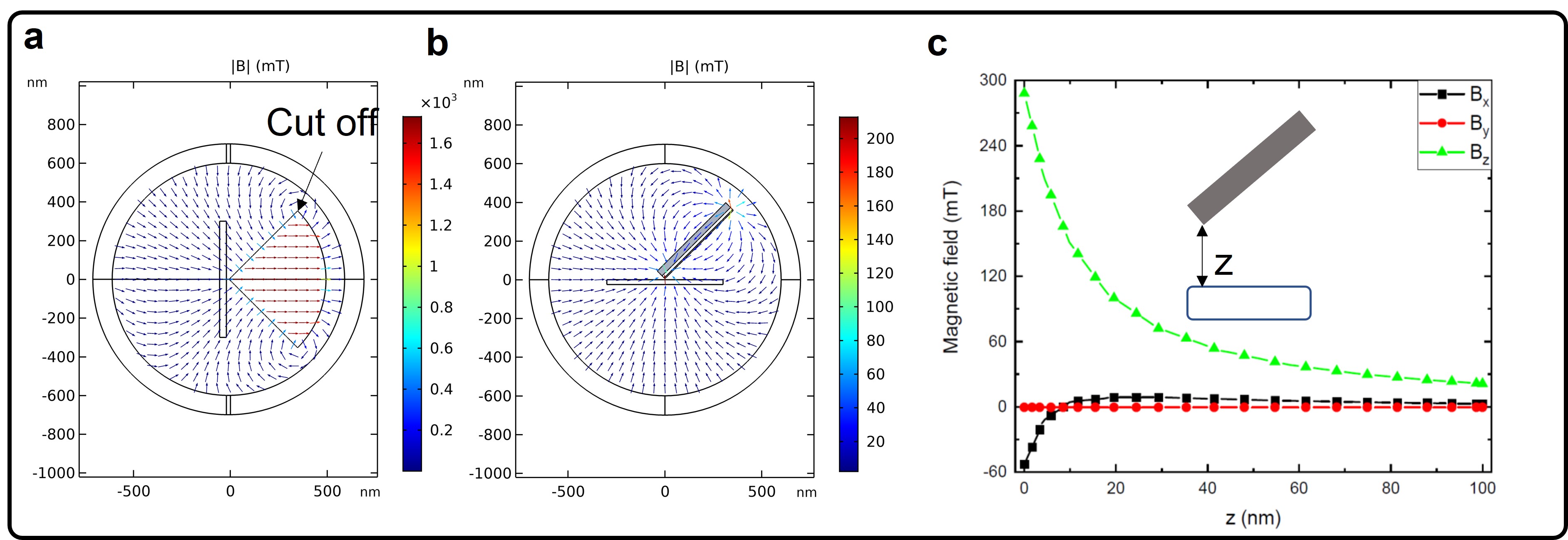
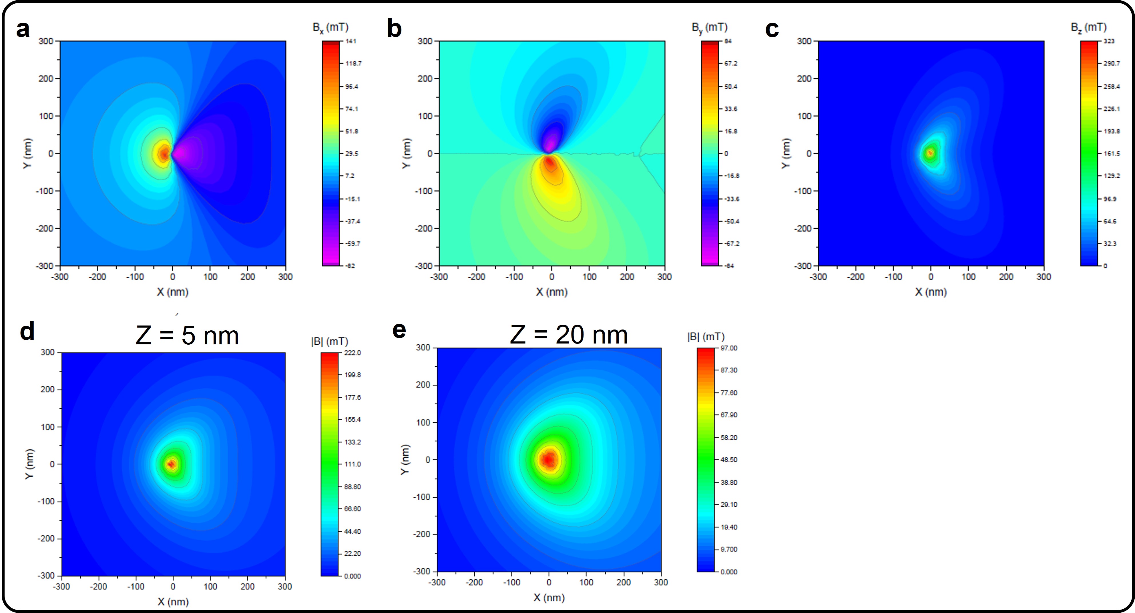
We calculated the spatial distribution of the tip’s stray field across the sample surface. Figure 11 shows the lateral distribution of , and at a tip-sample distance of . We expect this to be the closest tip-sample distance during oscillation. At the lowest point of the amplitude extension with respect to the sample surface, the stray field perturbation should be strongest. The and components in Figure 11a and 11b show sign inversion close to the (0,0) point, where the tip apex is positioned. This is to be expected from the symmetry of the planar probe. The magnitude of can become quite large up to . However, at (0,0) the field is minimal for . But for a sizable field up to is observed directly below the tip. For a fabricated planar probe, the tip is never fully symmetric, nor is the bridge shape and it’s position on the tip apex. The in-plane values are hence expected to be larger below the tip during experiments. The out-of-plane component is strongest at (0,0) and given in Figure 11c. The magnitude can reach up to over . For measuring LMO3, having both an in-plane and out-of-plane field is beneficial, as the SM-PP in-plane field magnetises the SP islands, while is used to read out the stray signal. This is similar to the SSM experiments of Anahory et al. 14 and supports our work on observing the complex SP islands.
We also examined the dependency of the magnetic field magnitude and distribution on , between and . The spatial distribution of is given in Figure 11d and 11e, respectively. Evidently, increases by almost a factor of as decreases down to . Hence, this may explain why we observe a sudden change (kink) in F-z spectroscopy, in Figure 4 in the main text, as the SP islands are magnetized and a sudden change in the magnitude of the attractive force occurs.
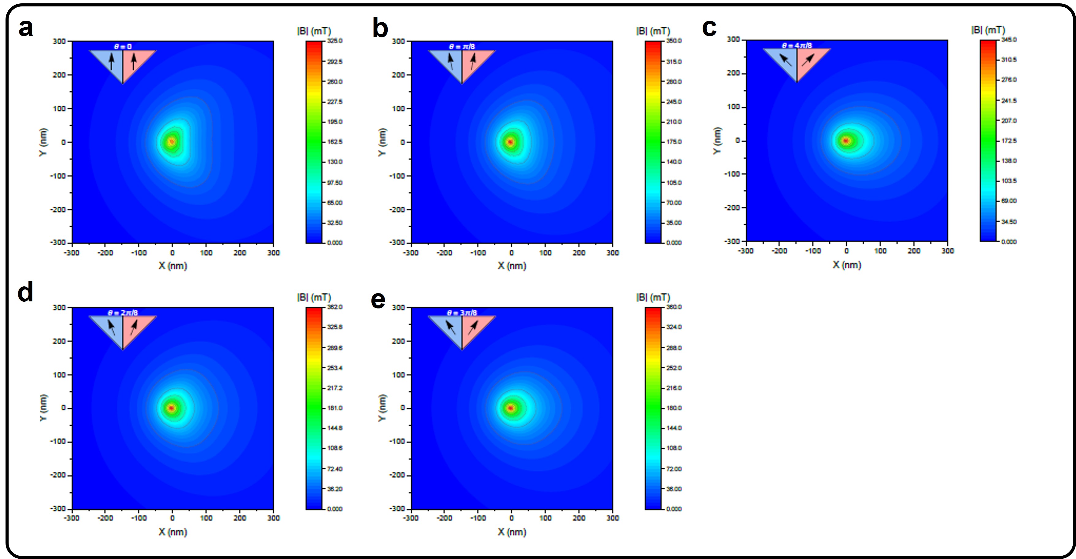
Finally, we examined the effect of the direction of the Co magnetisation along the planar probe symmetry axis, on the tip stray field magnitude and distribution. Figure 12 shows the calculated at a fixed . Here, the relative Co magnetisation direction on both sides of the symmetry axis are depicted in blue and red with the angle between the two directions indicated as . Two main conclusions can be derived from these results: the magnitude of magnetic field strength is relatively independent on . And secondly, the shape of the magnetic field distribution on the surface changes only slightly. In conclusion, changing the symmetry of Co magnetisation along the planar probe vertical symmetry axis does not alter the final distribution a lot. Hence it is reasonable to assume is mainly tip-sample distance , dependent.
0.8 Supplementary S5: Methods SM-PP MFM experiment
0.8.1 LMO3 sample in UHV
The 6 u.c. LMO3/STO3 sample was exposed to ambient air prior to measurement, hence we expect a thin layer of contaminates present of the LMO3 surface before being loaded into UHV. Gently heating to in UHV removed the water adsorbents. Higher temperatures were not used to prevent oxygen diffusion which likely alters the stochiometry and magnetic behaviour 32, 33. However, we cannot attest if small stochiometric changes have occurred (and also over time) or between sample growths. This variable offers future investigation possibilities between the stochiometry relationship and the magnetic textures.
0.8.2 FM-MFM imaging and data visualisation
To measure the long-range MFM signal, the tip was retracted by and followed the previously obtained topography, the so-called lift mode 1. For measuring the long range magnetic gradient force , the oscillation amplitude was set to .
A Scienta Omicron VT-SPM was used with a custom tip holder and low temperature sample holder for enhanced thermal conduction. Imaging was performed by locking the amplitude and tracking the frequency shift with a phase lock loop (PLL). Care was taken to keep all the scanning parameters constant, with optimized feedback settings for the phase, amplitude and frequency. The PLL bandwidth was set to . After a topography line-scan was obtained, the tip was lifted by the predefined lift height. Both forward and backward scans where compared to identify repeatability and exclude artifacts. We imaged with a speed of at a resolution of 256x256 pixels. Gwyddion software was used for the AFM and MFM data plotting and analysis. We used plane projection to level the image, and line-alignment in the vertical direction. Due to thermal drift induced by the thermal gradient between the cold sample and the room temperature SM-PP (as dictated by the VT-SPM design), a small eigenmode frequency shift of was observed during the prolonged imaging, hence we renormalized the frequency MFM shift accordingly to the first few line-scans. No influence on the MFM lateral dimensions was noted by this effect. Finally, both the sample and tip are grounded. Future work will translate the SM-PP to a cryostat to reduce thermal gradients which would also significantly increase the further.
0.9 Supplementary S6: Variable temperature MFM
References
- Kazakova et al. 2019 Kazakova, O.; Puttock, R.; Barton, C.; Corte-León, H.; Jaafar, M.; Neu, V.; Asenjo, A. Frontiers of magnetic force microscopy. Journal of Applied Physics 2019, 125, 60901
- Hug et al. 1998 Hug, H. J.; Stiefel, B.; Van Schendel, P. J.; Moser, A.; Hofer, R.; Martin, S.; Güntherodt, H. J.; Porthun, S.; Abelmann, L.; Lodder, J. C.; Bochi, G.; O’Handley, R. C. Quantitative magnetic force microscopy on perpendicularly magnetized samples. Journal of Applied Physics 1998, 83, 5609–5620
- Casiraghi et al. 2019 Casiraghi, A.; Corte-León, H.; Vafaee, M.; Garcia-Sanchez, F.; Durin, G.; Pasquale, M.; Jakob, G.; Kläui, M.; Kazakova, O. Individual skyrmion manipulation by local magnetic field gradients. Communications Physics 2019, 2, 1–10
- Albisetti et al. 2016 Albisetti, E.; Petti, D.; Pancaldi, M.; Madami, M.; Tacchi, S.; Curtis, J.; King, W. P.; Papp, A.; Csaba, G.; Porod, W.; Vavassori, P.; Riedo, E.; Bertacco, R. Nanopatterning reconfigurable magnetic landscapes via thermally assisted scanning probe lithography. Nature Nanotechnology 2016, 11, 545–551
- Gartside et al. 2018 Gartside, J. C.; Arroo, D. M.; Burn, D. M.; Bemmer, V. L.; Moskalenko, A.; Cohen, L. F.; Branford, W. R. Realization of ground state in artificial kagome spin ice via topological defect-driven magnetic writing. Nature Nanotechnology 2018, 13, 53–58
- Schreiber et al. 2008 Schreiber, S.; Savia, M.; Pelekhov, D. V.; Iscru, D. F.; Selcu, C.; Hammel, P. C.; Agarwal, G. Magnetic force microscopy of superparamagnetic nanoparticles. Small 2008, 4, 270–278
- Torre et al. 2011 Torre, B.; Bertoni, G.; Fragouli, D.; Falqui, A.; Salerno, M.; Diaspro, A.; Cingolani, R.; Athanassiou, A. Magnetic force microscopy and energy loss imaging of superparamagnetic iron oxide nanoparticles. Scientific Reports 2011, 1
- Angeloni et al. 2016 Angeloni, L.; Passeri, D.; Reggente, M.; Mantovani, D.; Rossi, M. Removal of electrostatic artifacts in magnetic force microscopy by controlled magnetization of the tip: Application to superparamagnetic nanoparticles. Scientific Reports 2016, 6, 1–14
- Krivcov et al. 2018 Krivcov, A.; Junkers, T.; Möbius, H. Understanding electrostatic and magnetic forces in magnetic force microscopy: Towards single superparamagnetic nanoparticle resolution. Journal of Physics Communications 2018, 2
- Cambel et al. 2011 Cambel, V.; Gregušová, D.; Eliáš, P.; Fedor, J.; Kostič, I.; Maňka, J.; Ballo, P. Switching magnetization magnetic force microscopy - An alternative to conventional lift-mode MFM. Journal of Electrical Engineering 2011, 62, 37–43
- Cambel et al. 2013 Cambel, V.; Precner, M.; Fedor, J.; Šoltýs, J.; Tóbik, J.; Ščepka, T.; Karapetrov, G. High resolution switching magnetization magnetic force microscopy. Applied Physics Letters 2013, 102, 1–5
- Wren et al. 2017 Wren, T.; Puttock, R.; Gribkov, B.; Vdovichev, S.; Kazakova, O. Switchable bi-stable multilayer magnetic probes for imaging of soft magnetic structures. Ultramicroscopy 2017, 179, 41–46
- Wang et al. 2015 Wang, X. R.; Li, C. J.; Lü, W. M.; Paudel, T. R.; Leusink, D. P.; Hoek, M.; Poccia, N.; Vailionis, A.; Venkatesan, T.; Coey, J. M.; Tsymbal, E. Y.; Ariando,; Hilgenkamp, H. Imaging and control of ferromagnetism in LaMnO3/SrTiO3 heterostructures. Science 2015, 349, 716–719
- Anahory et al. 2016 Anahory, Y.; Embon, L.; Li, C. J.; Banerjee, S.; Meltzer, A.; Naren, H. R.; Yakovenko, A.; Cuppens, J.; Myasoedov, Y.; Rappaport, M. L.; Huber, M. E.; Michaeli, K.; Venkatesan, T.; Ariando,; Zeldov, E. Emergent nanoscale superparamagnetism at oxide interfaces. Nature Communications 2016, 7
- Corte-León et al. 2019 Corte-León, H.; Rodríguez, L. A.; Pancaldi, M.; Gatel, C.; Cox, D.; Snoeck, E.; Antonov, V.; Vavassori, P.; Kazakova, O. Magnetic imaging using geometrically constrained nano-domain walls. Nanoscale 2019, 11, 4478–4488
- Sakar et al. 2021 Sakar, B.; Liu, Y.; Sievers, S.; Neu, V.; Lang, J.; Osterkamp, C.; Markham, M. L.; Öztürk, O.; Jelezko, F.; Schumacher, H. W. Quantum calibrated magnetic force microscopy. Physical Review B 2021, 104, 1–6
- Siahaan et al. 2015 Siahaan, T.; Kurnosikov, O.; Barcones, B.; Swagten, H. J.; Koopmans, B. Cleaved thin-film probes for scanning tunneling microscopy. Nanotechnology 2015, 27
- Ciftci et al. 2019 Ciftci, H. T.; Van, L. P.; Koopmans, B.; Kurnosikov, O. Polymer patterning with self-heating atomic force microscope probes. Journal of Physical Chemistry A 2019, 123, 8036–8042
- 19 Leeuwenhoek, M.; Groenewoud, F.; Van Oosten, K.; Benschop, T.; Allan, M. P.; Gröblacher, S. Fabrication of on-chip probes for double-tip scanning tunneling microscopy.
- Çiftçi et al. 2022 Çiftçi, H. T.; Verhage, M.; Cromwijk, T.; Pham Van, L.; Koopmans, B.; Flipse, K.; Kurnosikov, O. Enhancing sensitivity in atomic force microscopy for planar tip-on-chip probes. Microsystems & Nanoengineering 2022, 8
- Schneiderbauer et al. 2012 Schneiderbauer, M.; Wastl, D.; Giessibl, F. J. qPlus magnetic force microscopy in frequencymodulation mode with millihertz resolution. 2012
- Dagdeviren and Schwarz 2017 Dagdeviren, O. E.; Schwarz, U. D. Optimizing qPlus sensor assemblies for simultaneous scanning tunneling and noncontact atomic force microscopy operation based on finite element method analysis. Beilstein J. Nanotechnol 2017, 8, 657–666
- Ooe et al. 2014 Ooe, H.; Sakuishi, T.; Nogami, M.; Tomitori, M.; Arai, T. Resonance frequency-retuned quartz tuning fork as a force sensor for noncontact atomic force microscopy. Applied Physics Letters 2014, 105
- Giessibl 2019 Giessibl, F. J. The qPlus sensor, a powerful core for the atomic force microscope. Review of Scientific Instruments 2019, 90
- Gambardella et al. 2014 Gambardella, A.; Graziosi, P.; Bergenti, I.; Prezioso, M.; Pullini, D.; Milita, S.; Biscarini, F.; Dediu, V. A. Surface nanostructures in manganite films. Scientific Reports 2014, 4, 1–5
- Casola et al. 2018 Casola, F.; Van Der Sar, T.; Yacoby, A. Probing condensed matter physics with magnetometry based on nitrogen-vacancy centres in diamond. Nature Reviews Materials 2018, 3
- Healey et al. 2023 Healey, A. J.; Scholten, S. C.; Yang, T.; Scott, J. A.; Abrahams, G. J.; Robertson, I. O.; Hou, X. F.; Guo, Y. F.; Rahman, S.; Lu, Y.; Kianinia, M.; Aharonovich, I.; Tetienne, J. P. Quantum microscopy with van der Waals heterostructures. Nature Physics 2023, 19, 87–91
- Ariyaratne et al. 2018 Ariyaratne, A.; Bluvstein, D.; Myers, B. A.; Jayich, A. C. Nanoscale electrical conductivity imaging using a nitrogen-vacancy center in diamond. Nature Communications 2018, 9, 1–7
- Lei et al. 2012 Lei, W.-S.; Kumar, A.; Yalamanchili, R. Die singulation technologies for advanced packaging: A critical review. Journal of Vacuum Science & Technology B, Nanotechnology and Microelectronics: Materials, Processing, Measurement, and Phenomena 2012, 30, 040801
- Slifka et al. 1998 Slifka, A. J.; Filla, B. J.; Phelps, J. M. Thermal Conductivity of Magnesium Oxide from Absolute, Steady-State Measurements. Journal of Research of the National Institute of Standards and Technology 1998, 103, 357–363
- Vansteenkiste et al. 2014 Vansteenkiste, A.; Leliaert, J.; Dvornik, M.; Helsen, M.; Garcia-Sanchez, F.; Van Waeyenberge, B. The design and verification of MuMax3. AIP Advances 2014, 4
- Li et al. 2019 Li, M. et al. Controlling the Magnetic Properties of LaMnO3/SrTiO3 Heterostructures by Stoichiometry and Electronic Reconstruction: Atomic-Scale Evidence. Advanced Materials 2019, 31
- Xie et al. 2015 Xie, H.; Huang, H.; Cao, N.; Zhou, C.; Niu, D.; Gao, Y. Effects of annealing on structure and composition of LSMO thin films. Physica B: Condensed Matter 2015, 477, 14–19