SReferences Supplementary Materials
Magnetic switching of spin-scattering centers in Dresselhaus [110] circuits
Abstract
Spin carriers subject to Dresselhaus [110] (D110) spin-orbit coupling (SOC) gather null spin phases in closed circuits, contrary to usual Rashba and Dresselhaus [001] SOC. We show that D110 spin phases can be activated in square circuits by introducing an in-plane Zeeman field, where localized field inhomogeneities act as effective spin-scattering centers. Our simulations show rich interference patterns in the quantum conductance, which work as maps for a geometric classification of the propagating spin states. We also find that disorder facilitates low-field implementations.
Introduction. — Spin-orbit coupling (SOC) in two-dimensional electron gases (2DEG) [1] is a strategic resource for quantum electronics and spin-based technologies [2, 3, 4, 5]. The cases of Rashba [6] and Dresselhaus [001] [7] SOC in zincblende III-V compound semiconductor quantum wells have been discussed extensively in the literature over the last decades. Although they belong to different symmetry classes, both Rashba and Dresselhaus [001] SOC present in-plane effective field textures exploited in, e.g., Aharonov-Casher (AC) spin interferometry [8, 9, 10, 11, 12, 13, 14, 15, 16, 17, 18, 19, 20] and the manipulation of geometric spin phases in electronic transport [21, 11, 17, 22, 23] by electrical control of the corresponding SOC strengths [24, 25, 18]. By contrast, Dresselhaus [110] (D110) SOC [7] has received relatively little attention (with some notable exceptions [1, 26, 27, 28, 29, 30, 4, 31, 32]). However, D110 offers a unique feature of practical interest: an effective field texture perpendicular to the 2DEG’s plane. Such a robust symmetry facilitates the development of a so-called persistent spin helix (PSH) [31, 33, 34] and the corresponding suppression of spin relaxation [27], spin dephasing [35], spin Hall effect [36], and weak antilocalization [26] for conduction electrons. One additional consequence of utmost importance is the absence of AC interference in D110 systems, as in any PSH. This is true not only for III-V compound semiconductor 2DEGs but also for group III and IV monochalcogenide monolayers. Moreover, D110 has been proposed for realizing topological phases in noncentrosymmetric superconductors that could host the celebrated (and elusive) Majorana modes [32].
In this article, we discuss D110-based spin interferometry and control in mesoscopic circuits of square shape. Due to its symmetry properties, D110 alone does not manifest any sign of AC interference in electronic transport. We show that the introduction of an additional in-plane Zeeman field activates complex spin dynamics leading to the development of spin phases and interference effects that modulate the quantum conductance. In polygonal circuits, the interplay between D110 and Zeeman fields creates effective-field discontinuities localized at the vertices where spin-scattering takes place. This results in field-dependent phase differences between counter-propagating spin carriers that produce a rich interference pattern. The effect is remarkable, as it enables the magnetic switching of spin-scattering centers in D110 circuits (difficult to achieve with other SOC classes) and its characterization by means of transport experiments. Furthermore, we show that this result is robust against disorder and realizable at low field strengths thanks to the Al’tshuler-Aronov-Spivak (AAS) effect [37].
Here, we focus on the modelling of square D110 circuits built on 2DEG lodged in III-V semiconductor heterostructures. Other geometries may work as well; still, we choose square circuits based on its simple experimental realization, modelling, numerical simulation, and interpretation. Previous works have shown that rich conductance patterns arise in Rashba squares [38, 39, 40]. Moreover one-dimensional (1D) models have been applied with success to Rashba squares [41, 42, 43, 44, 45], resulting in excellent agreement with the experimental observations. One-dimensional models are especially suited to large loop arrays [13, 38, 17, 22, 18, 40], where higher slow-propagating modes are more likely to decohere than lower fast-propagating ones. The surviving interference observed in experiments with loop arrays is well described by the physics of one single (quasi 1D) orbital mode propagating along a single mesoscopic loop [17, 22, 18, 40, 23].
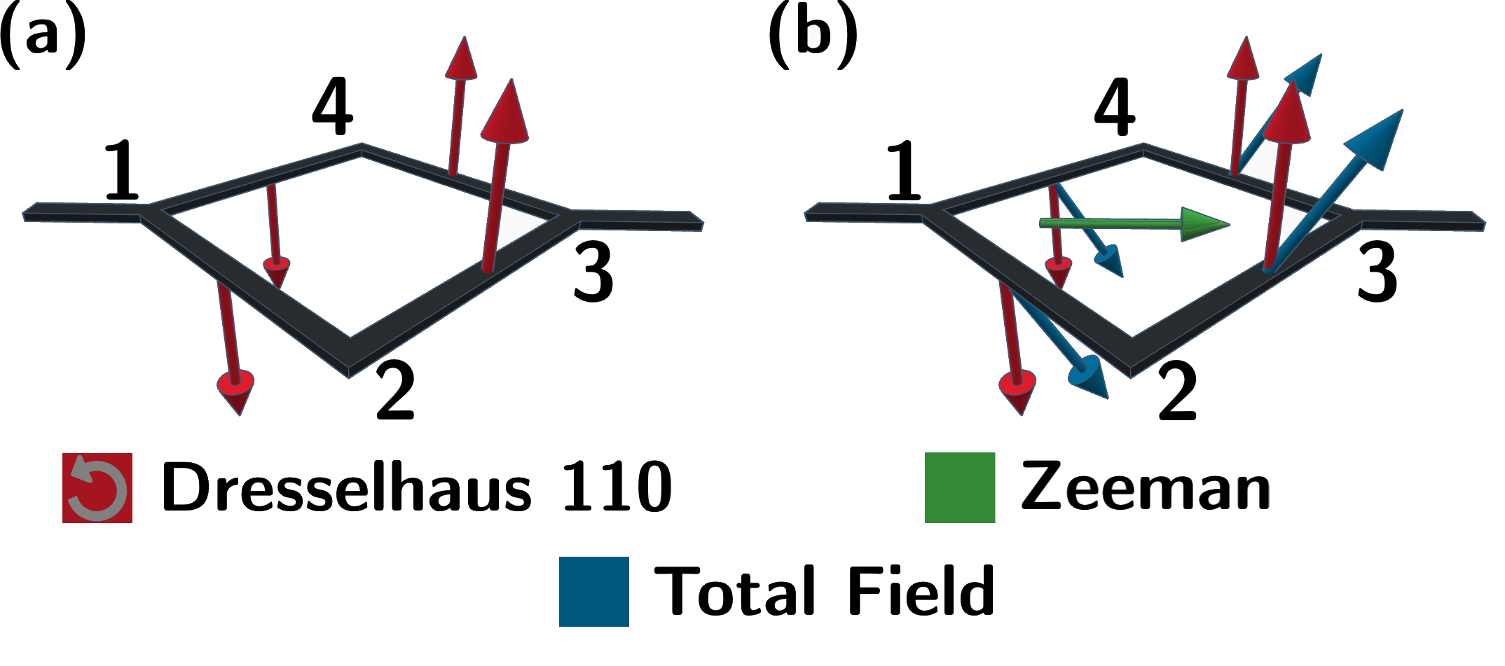
Model — We consider a 1D square circuit contained in the -plane consisting of conducting segments of length subject to D110 SOC and Zeeman coupling, see Fig. 1. Each segment connects vertices and and is oriented along the direction , from towards . The spin-carrier dynamics along each segment is given by the Hamiltonian [1, 29, 30, 4, 31]:
| (1) |
where is the carrier’s linear momentum along , is the linear D110 SOC strength, the carrier’s effective mass, is the magnetic moment, and the vector of Pauli matrices. Notice that the D110 SOC contribution —2nd term on the r.h.s. of Eq. (1) —appears as a momentum-dependent magnetic field of magnitude coupled to the spin along the direction. Importantly, since , the orientation of each segment modulates the amplitude and sign of the D110 SOC strength. This term establishes a PSH [31, 33, 34]. There is experimental evidence [46] of a dominating linear-in-momentum contribution to D110 SOC 111Notice that the lesser higher-order contribution proportional to [4], with the polar angle with respect to the axis, does not compromize the PSH since it acts along the axis as well as the linear contribution in Eq. (1).. Still, higher-order contributions can be incorporated by introducing a renormalized in Eq. (1) [4]. This suggest the possibility of controlling the D110 SOC strength by electrical means, similar to what recently found in Dresselhaus [001] systems [25, 18]. The in-plane Zeeman field, , with , is common to all segments. Hence, the effective field undergone by a spin-carrier travelling either clockwise (CW) or counterclockwise (CCW) around the square loop resembles a stroboscopic Rabi driving, namely, a constant Zeeman field coexisting with a normal D110 component that takes a sequence of discrete values, see Fig. 1(b). Notice that the Zeeman field undermines the PSH established by the D110 SOC field.
The square circuit of Fig. 1 is oriented such that, starting from node , the directional angles are . This choice maximizes the amplitude of the D110 SOC field. The resulting D110 field texture for a spin carrier travelling CCW is shown in Fig. 1(a). It represents a field oscillating along the direction, fixing a global spin quantization axis. Under this circumstance, the spin phase gathered by a carrier in a round trip is zero. Figure 1(b) shows how the introduction of an external in-plane Zeeman field induces sudden changes in the direction of the effective-field at nodes and , destroying the global quantization axis. This favors the development of complex spin dynamics and phases due to the misalignment of the local spin quantization axis at different segments. In this way, vertices and act as effective spin-scattering centers. In order to maximize interference effects, in the following we study quantum transport between vertices and . Any other choice would undermine spin-dependent signatures (in particular, symmetry dictates that flat interference patterns are expected for transport between nodes and ). Still, misalignments up to between the leads and the crystallographic axis are acceptable. See Supplemental Material.
To study the quantum conductance as a function of D110 and Zeeman fields we implement a tight-binding model of the square loop and use a Green’s function formalism. This permits the inclusion of contact leads and accounts for all possible propagation paths contributing to quantum transport between contacts (see Supplemental Material). Following the Landauer-Büttiker formalism [48], the zero-temperature conductance is given by , with the quantum transmission between contacts evaluated at the Fermi energy, . Notice that a suitable description of the experimental conditions requires a Fermi energy average of the computed conductance to discard resonances due to finite-size effects. We focus on the semiclassical limit in which the Fermi wavelength of the electron, , with the Fermi momentum, is much smaller than the perimeter , i.e., [22, 11].
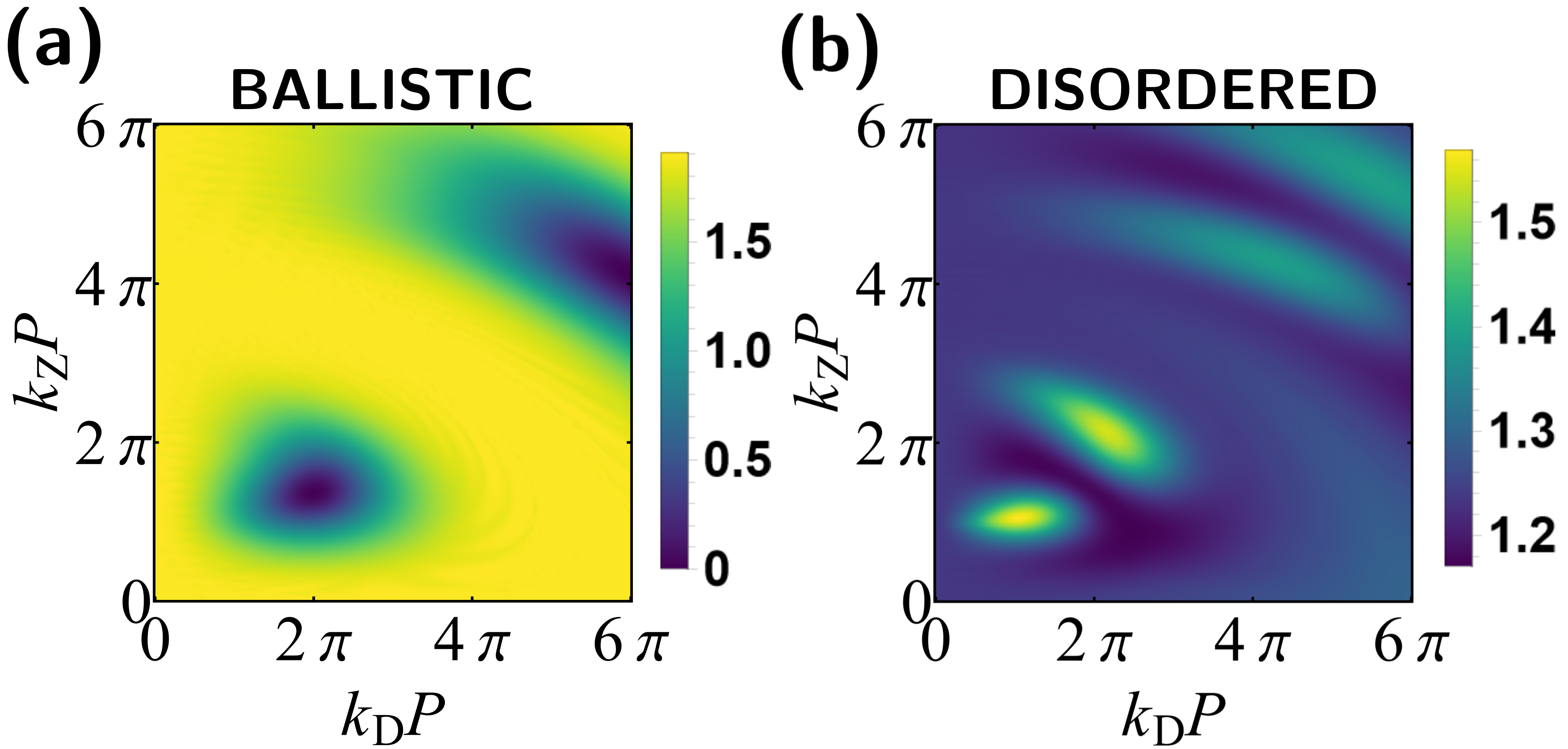
Results — In Figure 2 we show the computed conductance as a function of and . These parameters are chosen to coincide with the spin phases gathered by a spin carrier propagating along a straight quantum wire of length oriented along the -axis due to the action of the D110 and Zeeman fields, respectively, with a flight time . Figure 2(a) shows results for a symmetric square identified with ballistic transport through a regular array of square loops. Notice, however, that a typical sample consists of hundreds of loops, so that a more realistic description of the experimental conditions requires a self-averaging over disorder realizations (modelled here by introducing segments of fluctuating lengths taken from a random distribution). We plot the corresponding tight-binding results in Figure 2(b).
Our numerical simulations show that spin interference effects appear as periodic patterns in the quantum conductance over a wide range of field strengths. However, here we focus our attention on relatively low and values, according to the limited field strengths accessible in experiments [22, 40]. In both cases— ballistic, Fig. 2(a), and disordered, Fig. 2(b)— we observe that the coexistence of D110 and Zeeman fields is essential for the emergence of spin interference effects: D110 or Zeeman fields alone do not imprint any relevant spin phase contributing to interference due to the existence of global spin quantization axes (along and , respectively) and the conductance is spin independent.
In contrast, the interplay between D110 and Zeeman fields produces discontinuities in the direction of the local spin-quantization axis at vertices 2 and 4, Fig. 1(b), that turn on spin-scattering processes and spin phases contributing to interference. When both fields are comparable in magnitude, spin interference leads to a periodic series of lobes corresponding to minimum, Fig. 2(a), or maximum, Fig. 2(b), conductance. Notice that disordered circuits display split lobes with respect to the ballistic case, with a periodicity of order along the diagonal . The lobe splitting is a manifestation of the AAS effect [37] due to dominant time-reversed interfering paths in disordered loops, also related to weak-(anti)localization in disordered thin layers [49, 50]. This has dramatic consequences for experimental verification, since it allows for detection of active field discontinuities for lower field magnitudes if one focuses on the first split lobe.
In-plane magnetic fields of 2.5T lead to in square loops with perimeter m built on 2DEGs lodged in InGaAs quantum wells (QW) [40] . Moreover, in single-mode QWs of width one can approximate [29], with the bulk-inversion asymmetry coefficient running from 11 eVÅ3 in GaAs and InGaAs [51] to 490 eVÅ3 in InSb [52]. The QWs can be as narrow as 5-10 nm [25, 29]. Moreover, the carriers’ effective mass runs from 0.014 in InSb to 0.023 in InAs, 0.041 in InGaAs, and 0.067 in GaAs (in units of the electron mass ) [1]. To be conservative, for square loops with m built on a nm InGaAs QW we find . These values could be tuned on the same sample by building arrays of square loops with different perimeter , to be tested in transport experiments. The electrical tuning of the renormalized (through cubic terms) can also contribute with a tuning range proportional to [18, 25].
We point out that the interference patterns shown in Fig. 2 for D110 squares are essentially different from those reported in Ref. [40] for Rashba squares. There, the Rashba SOC lead to AC interference patterns subject to additional modulation by an in-plane Zeeman field (with lobes centered on the Rashba axis). Here, instead, no AC interference arises as a consequence of D110 SOC: both D110 and Zeeman fields are necessary for the emergence of interference patterns (with no lobes on the D110 axis).
Finally, the conductance shows no dependence on , namely, the results of Figs. 2(a) and 2(b) are valid for any orientation of the in-plane Zeeman field (see Supplemental Material for a demonstration).
Discussion. — To gain further physical insight on the exact numerical results presented above, we make use of a 1D model that captures the spin dynamics along the loop, disregarding orbital back-scattering at the vertices [40, 44]. The solutions of the 1D Schrödinger equation along a segment based on (1) are plane waves such that the spinor wavefunction propagates from vertex towards vertex along the direction as
| (2) |
where parametrizes the distance from vertex , with at vertex . The prefactor corresponds to the kinetic phase of the carrier associated to the charge dynamics, while the remaining factors represent the spin phase due to spin precession in the presence of D110 and Zeeman fields. Notice that the D110 SOC field inverts its sign for counter-propagating carriers. Indeed, since points from to , the sign reversal of the D110 contribution is made explicit in Eq. (2) by noting that .
According to Eq.(2), the spin evolution along a full segment is given by the spin rotation operator:
| (3) |
By using the labelling shown in Figs. 3(a) and 3(b), we define the spin evolution operators , , and , with the subindex () indicating CCW (CW) propagation. The unitary represent full round-trips with origin in vertex 1, whereas correspond to direct paths from vertex 1 to vertex 3. We resort again to the Landauer-Büttiker formalism and obtain the conductance, , by computing the transmission for two different dominating interference processes. In the first case, is computed from the interference between the direct paths and , see Fig. 3(a). This contribution is dominant for geometries preserving a twofold reflection symmetry along the axis connecting the contact leads. It requires symmetric and clean samples as, e.g., the ballistic ones discussed in Fig. 2(a). In the second case, the transmission is computed as after noting that the reflection coefficient follows from the interference between paths and , see Fig. 3(b). This contribution dominates in disordered samples, as those discussed in Fig. 2(b), since and describe the spin evolution along time-reversed paths.
Figures 3(c) and 3(d) show the conductances and calculated from direct and time-reversed path contributions, respectively, as a function of and . We find that these lower-order semiclassical models reproduce very well the fully quantum numerical results of Fig. 2 for the ballistic () and disordered () cases. In particular, the agreement between the disordered tight-binding simulations, Fig. 2(b), and the results from time-reversed path contributions, Fig. 3(d), demonstrates that the lobe splitting has its origin in the AAS effect.
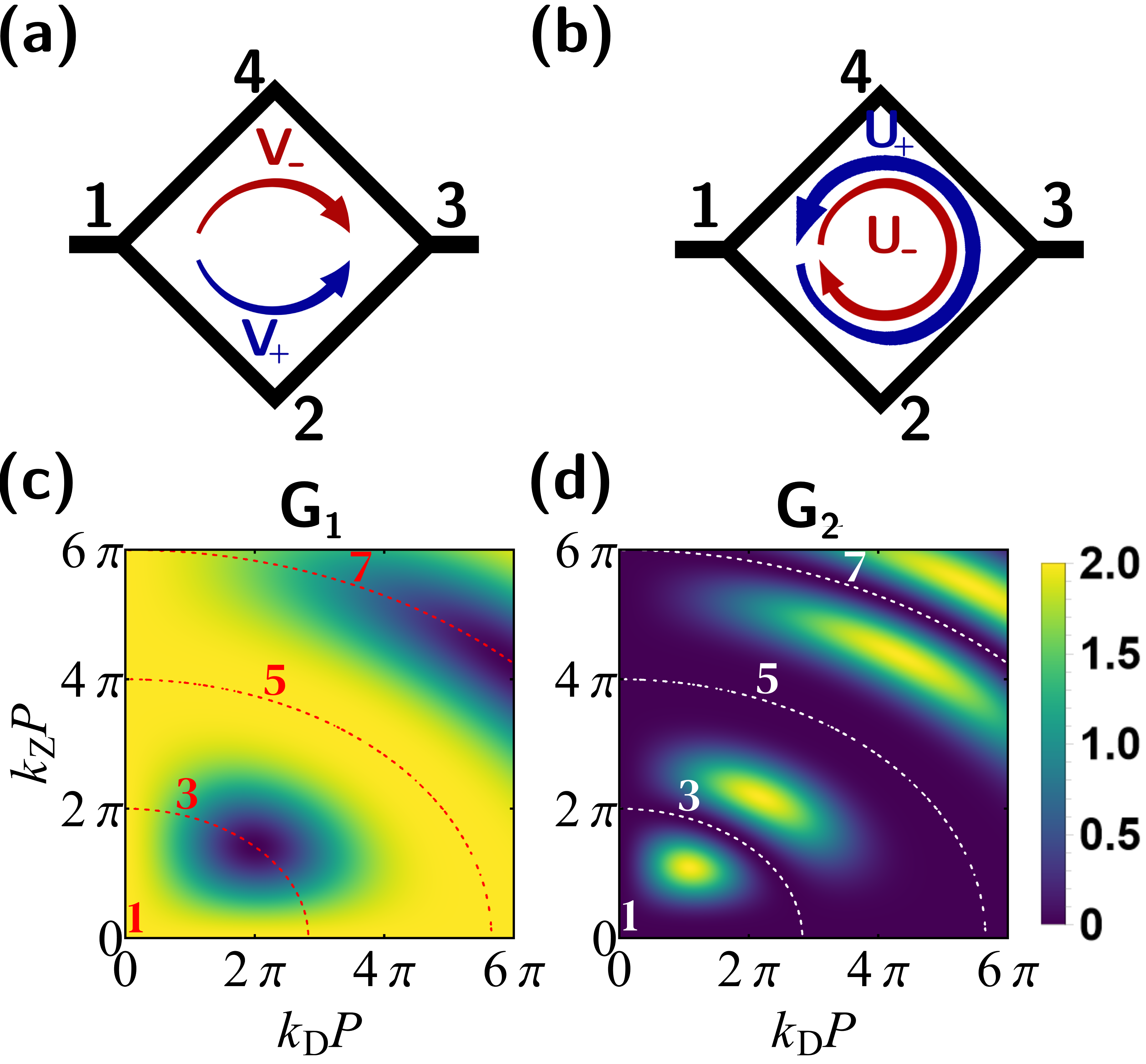
Moreover, an inspection of unveils relevant geometric characteristics of the spin states. We find that reduces to the SU(2) identity whenever , with and integer. Notice that the carriers gather no net spin phase in a full round trip for these particular field settings. The condition defines a series of lines that split the lobes in Figs. 3(c) and 3(d). Interestingly, we find that such lines also define topological transitions for the textures displayed by the spin modes in the Bloch sphere (with an eigen-solution of ). This is demonstrated by defining the winding number around the Zeeman-field axis as
| (4) |
where is the normalized projection of the spin texture on the plane orthogonal to (see Supplemental Material for further details). We find that the spin states organize in sectors with definite odd , with only one single lobe per sector in Figs. 3(d). This finding suggest that the interference pattern in the quantum conductance can work as a map for the geometric characterization of the spin states.
Conclusions and Outlook. — We show that the combined action of D110 SOC and Zeeman fields is a resourceful tool for the manipulation of spin carriers in quantum circuits. This is demonstrated in square circuits as a proof of concept, though other geometries may work as well. When either field dominates over the other, transport is spin independent (differing form previous results with Rashba squares displaying AC interference [40]). By contrast, the application of D110 and Zeeman fields of similar magnitude turns on effective spin-scattering centers that trigger complex spin dynamics and the development of spin phases modulating quantum transport. The resulting interference pattern in the conductance works as a guide through the geometry of the propagating spin states. Remarkably, the presence of disorder facilitates the experimental realization in loop arrays at relatively low field strengths due to the AAS effect. This also provides a way to determine the magnitude of the D110 SOC strength in a 2DEG.
Our results provide crucial information about the action of D110 SOC fields on spin carriers and show how spin dynamics can be activated in a controlled fashion, demonstrating a potential for applications in spintronics and spin-based quantum technologies.
We further notice some alternative implementations. Similar effects could be found in usual Rashba and Dresselhaus [001] square circuits (with in-plane effective SOC fields) provided that a PSH is established by setting equal SOC strengths [4]. This, however, has the disadvantage of requiring a fine tuning of the SOC fields (contrary to D110 circuits where the PSH is built-in). Moreover, group-III metal-monochalcogenide monolayers such as GaSe and GaS display threefold symmetric, cubic-in-momentum D110 [53] which could be optimally exploited by using, e.g., triangular or hexagonal circuits. Recently, it has been suggested [54] that group-IV monochalcogenide monolayers (Sn or Ge and S, Se, or Te) develop D110 PSHs originated by in-plane ferroelectricity that can be controlled electrically, appearing as possible platforms. An interesting alternative would be electron spin resonance (ESR) experiments in D110 zigzag ballistic channels instead of D110 square loops [55].
Acknowledgements. —
We acknowledge support from the Spanish MICINN-AEI through Project No. PID2021-127250NB-I00 and from the Andalusian Government through PAIDI 2020 Project No. P20-00548 and FEDER Project No. US-1380932. We thank R. Winkler for suggesting us the study of D110 circuits.
References
- Winkler [2003] R. Winkler, Spin—Orbit Coupling Effects in Two-Dimensional Electron and Hole Systems (Springer Berlin Heidelberg, 2003).
- Bercioux and Lucignano [2015] D. Bercioux and P. Lucignano, Quantum transport in Rashba spin–orbit materials: a review, Reports on Progress in Physics 78, 106001 (2015).
- Manchon et al. [2015] A. Manchon, H. C. Koo, J. Nitta, S. M. Frolov, and R. A. Duine, New perspectives for Rashba spin–orbit coupling, Nat. Mater. 14, 871 (2015).
- Schliemann [2017] J. Schliemann, Colloquium: Persistent spin textures in semiconductor nanostructures, Rev. Mod. Phys. 89, 011001 (2017).
- Hirohata et al. [2020] A. Hirohata, K. Yamada, Y. Nakatani, I.-L. Prejbeanu, B. Diény, P. Pirro, and B. Hillebrands, Review on spintronics: Principles and device applications, J. Magn. Magn. Mater. 509, 166711 (2020).
- Rashba [1960] E. Rashba, Properties of semiconductors with an extremum loop. 1. Cyclotron and combinational resonance in a magnetic field perpendicular to the plane of the loop, Sov. Phys. Solid State 2, 1109 (1960).
- Dresselhaus [1955] G. Dresselhaus, Spin-Orbit Coupling Effects in Zinc Blende Structures, Phys. Rev. 100, 580 (1955).
- Aharonov and Casher [1984] Y. Aharonov and A. Casher, Topological quantum effects for neutral particles, Phys. Rev. Lett. 53, 319 (1984).
- Mathur and Stone [1992] H. Mathur and A. D. Stone, Quantum transport and the electronic Aharonov-Casher effect, Phys. Rev. Lett. 68, 2964 (1992).
- Nitta et al. [1999] J. Nitta, F. E. Meijer, and H. Takayanagi, Spin-interference device, Appl. Phys. Lett. 75, 695 (1999).
- Frustaglia and Richter [2004] D. Frustaglia and K. Richter, Spin interference effects in ring conductors subject to Rashba coupling, Phys. Rev. B 69, 235310 (2004).
- Molnár et al. [2004] B. Molnár, F. M. Peeters, and P. Vasilopoulos, Spin-dependent magneto transport through a ring due to spin-orbit interaction, Phys. Rev. B 69, 155335 (2004).
- Bergsten et al. [2006] T. Bergsten, T. Kobayashi, Y. Sekine, and J. Nitta, Experimental demonstration of the time reversal Aharonov-Casher effect, Phys. Rev. Lett. 97, 196803 (2006).
- König et al. [2006] M. König, A. Tschetschetkin, E. M. Hankiewicz, J. Sinova, V. Hock, V. Daumer, M. Schäfer, C. R. Becker, H. Buhmann, and L. W. Molenkamp, Direct observation of the Aharonov-Casher phase, Phys. Rev. Lett. 96, 076804 (2006).
- Grbić et al. [2007] B. Grbić, R. Leturcq, T. Ihn, K. Ensslin, D. Reuter, and A. D. Wieck, Aharonov-bohm oscillations in the presence of strong spin-orbit interactions, Phys. Rev. Lett. 99, 176803 (2007).
- Aharony et al. [2011] A. Aharony, Y. Tokura, G. Z. Cohen, O. Entin-Wohlman, and S. Katsumoto, Filtering and analyzing mobile qubit information via Rashba–Dresselhaus–Aharonov–Bohm interferometers, Phys. Rev. B 84, 035323 (2011).
- Nagasawa et al. [2012] F. Nagasawa, J. Takagi, Y. Kunihashi, M. Kohda, and J. Nitta, Experimental demonstration of spin geometric phase: Radius dependence of time-reversal aharonov-casher oscillations, Phys. Rev. Lett. 108, 086801 (2012).
- Nagasawa et al. [2018] F. Nagasawa, A. A. Reynoso, J. P. Baltanás, D. Frustaglia, H. Saarikoski, and J. Nitta, Gate-controlled anisotropy in Aharonov-Casher spin interference: Signatures of Dresselhaus spin-orbit inversion and spin phases, Phys. Rev. B 98, 245301 (2018).
- Lia and Tamborenea [2021] J. Lia and P. Tamborenea, Narrow quantum rings with general Rashba and Dresselhaus spin-orbit interactions, Phys. E: Low-Dimens. Syst. Nanostructures 126, 114419 (2021).
- Shekhter et al. [2022] R. I. Shekhter, O. Entin-Wohlman, M. Jonson, and A. Aharony, Magnetoconductance Anisotropies and Aharonov-Casher Phases, Phys. Rev. Lett. 129, 037704 (2022).
- Aronov and Lyanda-Geller [1993] A. G. Aronov and Y. B. Lyanda-Geller, Spin-orbit Berry phase in conducting rings, Phys. Rev. Lett. 70, 343 (1993).
- Nagasawa et al. [2013] F. Nagasawa, D. Frustaglia, H. Saarikoski, K. Richter, and J. Nitta, Control of the spin geometric phase in semiconductor quantum rings, Nat. Commun. 4, 1 (2013).
- Frustaglia and Nitta [2020] D. Frustaglia and J. Nitta, Geometric spin phases in Aharonov-Casher interference, Solid State Commun. 311, 113864 (2020).
- Nitta et al. [1997] J. Nitta, T. Akazaki, H. Takayanagi, and T. Enoki, Gate control of spin-orbit interaction in an inverted —n0.53Ga0.47As/—n0.52Al0.48as heterostructure, Phys. Rev. Lett. 78, 1335 (1997).
- Dettwiler et al. [2017] F. Dettwiler, J. Fu, S. Mack, P. J. Weigele, J. C. Egues, D. D. Awschalom, and D. M. Zumbühl, Stretchable Persistent Spin Helices in GaAs Quantum Wells, Phys. Rev. X 7, 031010 (2017).
- Hassenkam et al. [1997] T. Hassenkam, S. Pedersen, K. Baklanov, A. Kristensen, C. B. Sorensen, P. E. Lindelof, F. G. Pikus, and G. E. Pikus, Spin splitting and weak localization in (110) GaAs/As quantum wells, Phys. Rev. B 55, 9298 (1997).
- Ohno et al. [1999] Y. Ohno, R. Terauchi, T. Adachi, F. Matsukura, and H. Ohno, Spin Relaxation in GaAs(110) Quantum Wells, Phys. Rev. Lett. 83, 4196 (1999).
- Couto et al. [2007] O. D. D. Couto, F. Iikawa, J. Rudolph, R. Hey, and P. V. Santos, Anisotropic Spin Transport in (110) GaAs Quantum Wells, Phys. Rev. Lett. 98, 036603 (2007).
- Liu and Chang [2010] M. H. Liu and C. R. Chang, Anomalous spin Hall effects in Dresselhaus (110) quantum wells, Phys. Rev. B 82, 155327 (2010).
- Ganichev and Golub [2014] S. Ganichev and L. Golub, Interplay of Rashba/Dresselhaus spin splittings probed by photogalvanic spectroscopy –A review, Phys. Status Solidi (B): Basic Res. 251 (2014).
- Iizasa et al. [2018] D. Iizasa, D. Sato, K. Morita, J. Nitta, and M. Kohda, Robustness of a persistent spin helix against a cubic Dresselhaus field in (001) and (110) oriented two-dimensional electron gases, Phys. Rev. B 98, 165112 (2018).
- You et al. [2013] J. You, C. H. Oh, and V. Vedral, Majorana fermions in s-wave noncentrosymmetric superconductor with Dresselhaus (110) spin-orbit coupling, Phys. Rev. B 87, 054501 (2013).
- Chen and Chang [2008] S.-H. Chen and C.-R. Chang, Non-Abelian spin-orbit gauge: Persistent spin helix and quantum square ring, Phys. Rev. B 77, 045324 (2008).
- Bernevig et al. [2006] B. A. Bernevig, J. Orenstein, and S.-C. Zhang, Exact SU(2) Symmetry and Persistent Spin Helix in a Spin-Orbit Coupled System, Phys. Rev. Lett. 97, 236601 (2006).
- Poshakinskiy and Tarasenko [2013] A. V. Poshakinskiy and S. A. Tarasenko, Effect of Dresselhaus spin-orbit coupling on spin dephasing in asymmetric and macroscopically symmetric (110)-grown quantum wells, Phys. Rev. B 87, 235301 (2013).
- Hankiewicz et al. [2006] E. M. Hankiewicz, G. Vignale, and M. E. Flatté, Spin-Hall Effect in a [110] GaAs Quantum Well, Phys. Rev. Lett. 97, 266601 (2006).
- Altshuler et al. [1981] B. Altshuler, A. Aronov, and B. Spivak, The Aaronov-Bohm effect in disordered conductors, JETP Lett. 33, 94 (1981).
- Koga et al. [2006] T. Koga, Y. Sekine, and J. Nitta, Experimental realization of a ballistic spin interferometer based on the Rashba effect using a nanolithographically defined square loop array, Phys. Rev. B 74, 041302 (2006).
- Qu et al. [2011] F. Qu, F. Yang, J. Chen, J. Shen, Y. Ding, J. Lu, Y. Song, H. Yang, G. Liu, J. Fan, Y. Li, Z. Ji, C. Yang, and L. Lu, Aharonov-Casher effect in Bi2Se3 square-ring interferometers, Phys. Rev. Lett. 107, 016802 (2011).
- Wang et al. [2019] M. Wang, H. Saarikoski, A. A. Reynoso, J. P. Baltanás, D. Frustaglia, and J. Nitta, Geometry-Assisted Topological Transitions in Spin Interferometry, Phys. Rev. Lett. 123, 266804 (2019).
- Bercioux et al. [2005] D. Bercioux, D. Frustaglia, and M. Governale, Signatures of spin-related phases in transport through regular polygons, Phys. Rev. B 72, 113310 (2005).
- van Veenhuizen et al. [2006] M. J. van Veenhuizen, T. Koga, and J. Nitta, Spin-orbit induced interference of ballistic electrons in polygon structures, Phys. Rev. B 73, 235315 (2006).
- Hijano et al. [2021] A. Hijano, T. L. V. D. Berg, D. Frustaglia, and D. Bercioux, Quantum network approach to spin interferometry driven by Abelian and non-Abelian fields, Phys. Rev. B 103, 155419 (2021).
- Rodríguez and Frustaglia [2021] E. J. Rodríguez and D. Frustaglia, Nonmonotonic quantum phase gathering in curved spintronic circuits, Phys. Rev. B 104, 195308 (2021).
- Hijano et al. [2022] A. Hijano, E. J. Rodríguez, D. Bercioux, and D. Frustaglia, Spin-texture topology in curved circuits driven by spin-orbit interactions, arxiv:2209.11653 (2022).
- Chen et al. [2014] Y. S. Chen, S. Fält, W. Wegscheider, and G. Salis, Unidirectional spin-orbit interaction and spin-helix state in a (110)-oriented GaAs/(Al,Ga)As quantum well, Phys. Rev. B 90, 121304 (2014).
- Note [1] Notice that the lesser higher-order contribution proportional to [4], with the polar angle with respect to the axis, does not compromize the PSH since it acts along the axis as well as the linear contribution in Eq. (1).
- Büttiker et al. [1985] M. Büttiker, Y. Imry, R. Landauer, and S. Pinhas, Generalized many-channel conductance formula with application to small rings, Phys. Rev. B 31, 6207 (1985).
- Bergmann [1984] G. Bergmann, Weak localization in thin films: a time-of-flight experiment with conduction electrons, Phys. Rep. 107, 1 (1984).
- Meijer et al. [2005] F. E. Meijer, A. F. Morpurgo, T. M. Klapwijk, and J. Nitta, Universal Spin-Induced Time Reversal Symmetry Breaking in Two-Dimensional Electron Gases with Rashba Spin-Orbit Interaction, Phys. Rev. Lett. 94, 186805 (2005).
- Kohda and Salis [2017] M. Kohda and G. Salis, Physics and application of persistent spin helix state in semiconductor heterostructures, Semiconductor Science and Technology 32, 073002 (2017).
- Kallaher et al. [2010] R. L. Kallaher, J. J. Heremans, N. Goel, S. J. Chung, and M. B. Santos, Spin-orbit interaction determined by antilocalization in an insb quantum well, Phys. Rev. B 81, 075303 (2010).
- Li and Appelbaum [2015] P. Li and I. Appelbaum, Symmetry, distorted band structure, and spin-orbit coupling of group-III metal-monochalcogenide monolayers, Phys. Rev. B 92, 195129 (2015).
- Absor and Ishii [2019] M. A. U. Absor and F. Ishii, Intrinsic persistent spin helix state in two-dimensional group-IV monochalcogenide monolayers ( or Ge and , Se, or Te), Phys. Rev. B 100, 115104 (2019).
- Sanada et al. [2013] H. Sanada, Y. Kunihashi, H. Gotoh, K. Onomitsu, M. Kohda, J. Nitta, P. V. Santos, and T. Sogawa, Manipulation of mobile spin coherence using magnetic-field-free electron spin resonance, Nature Physics 9, 280 (2013).