Epitaxial growth and scanning tunneling microscopy of LiV2O4 thin films on SrTiO3(111)
Abstract
LiV2O4 is a mixed-valent spinel oxide and one of a few transition-metal compounds to host a heavy fermion phase at low temperatures. While numerous experimental studies have attempted to elucidate how its 3 electrons undergo giant mass renormalization, spectroscopic probes that may provide crucial hints, such as scanning tunneling microscopy (STM), remain to be applied. A prerequisite is atomically flat and pristine surfaces, which, in the case of LiV2O4, are difficult to obtain by cleavage of small, three-dimensional crystals. We report the epitaxial growth of LiV2O4 thin films with bulklike properties on SrTiO3(111) via pulsed laser deposition and stable STM imaging of the LiV2O4(111) surface. The as-grown films were transferred ex situ to a room-temperature STM, where subsequent annealing with optional sputtering in ultrahigh vacuum enabled compact islands with smooth surfaces and a hexagonal 11 atomic lattice to be resolved. Our STM measurements provide insights into growth mechanisms of LiV2O4 on SrTiO3(111), as well as demonstrate the feasibility of performing surface-sensitive measurements of this heavy fermion compound.
The mixed-valent spinel oxide LiV2O4 has drawn attention over the years as the first discovered example of a heavy fermion system with 3 electrons, instead of 4 or 5 electrons Kondo et al. (1997); Urano et al. (2000). A key feature of this compound is the geometric frustration experienced by both its spins and charges. The magnetic V atoms occupy a pyrochlore sublattice with corner-sharing tetrahedra, which engenders spin frustration in the presence of nearest-neighbor antiferromagnetic exchange Kessler and Sienko (1971). The nominal V3.5+ ions are further hindered from charge disproportionation into a 1:1 population of V3+ and V4+ species. In order to minimize the short-range Coulomb energy, the number of adjacent V3+-V4+ pairs should be maximized, in analogy to the Ising model. However, a macroscopic number of degenerate configurations exists on the pyrochlore sublattice, leading to charge frustration Anderson (1956). While in many other mixed-valent spinel oxides Verwey (1939); Matsuno et al. (2001); Yamada and Tanaka (1995); Okamoto et al. (2008); Browne et al. (2018), the frustration is eventually relieved by structural distortions coupled with spin, charge, and/or orbital orders, LiV2O4 remains cubic with equivalent V sites down to at least 4 K Chmaissem et al. (1997), with no signs of ordering.
At low temperatures, LiV2O4 exhibits a metallic phase that satisfies many hallmarks of the heavy fermion state seen in Kondo-lattice systems with electrons. The linear coefficient extracted from the electronic heat capacity has a sizeable value of 0.42 J/(mol K2) at 1 K Kondo et al. (1997), which implies a 25-fold enhancement of effective mass compared to the value predicted by first-principles calculations with the local density approximation Matsuno, Fujimori, and Mattheiss (1999). The spin susceptibility is also large and nearly constant at low temperatures. Together, and yield a Wilson ratio of 1.7 Kondo et al. (1997), which is close to the value of one for free electrons. Resistivity measurements of single crystals showed on cooling a downturn at 20–30 K from -linear-like behavior, followed by a -like temperature dependence characteristic of a Fermi liquid below 2 K Urano et al. (2000). From a fit of the resistivity to , Urano et al. Urano et al. (2000) estimated the Kadowaki-Woods ratio to be ( cm/K2) / [mJ/(mol K2)]2, which is comparable to that of other heavy fermion compounds with electrons. Despite these similarities, it is unclear how the 3 electrons in LiV2O4 can be mapped onto a Kondo lattice, or whether a distinct mechanism of mass enhancement is at play, and such questions have inspired a large number of experimental studies on bulk samples Kondo et al. (1997); Urano et al. (2000); Shimoyamada et al. (2006); Jönsson et al. (2007); Shimizu et al. (2012); Browne et al. (2020) and theoretical models Anisimov et al. (1999); Fulde et al. (2001); Burdin, Grempel, and Georges (2002); Fujimoto (2002); Hopkinson and Coleman (2002); Yamashita and Ueda (2003); Arita et al. (2007); Hattori and Tsunetsugu (2009).
Thin films of LiV2O4 grown by pulsed laser deposition (PLD) represent a nascent avenue to derive fresh insights into the heavy fermion enigma Yajima et al. (2021); Niemann et al. . Thin films are especially amenable to charge and lattice engineering, and both electrochemical Li intercalation Yajima et al. (2021) and epitaxial strain Niemann et al. have been shown to induce metal-to-insulator transitions in LiV2O4 films. The latter is especially revealing, as tensile strain in the (001) plane explicitly breaks the degeneracy of the V pyrochlore sublattice. The resulting emergence of a Verwey-type charge order in strained, tetragonal films strongly implies that the heavy fermion phase in cubic LiV2O4 is a charge-frustrated phase, and that intense charge fluctuations underlie the giant mass renormalization of its 3 electrons Niemann et al. . Thin films are also amenable to angle-resolved photoemission spectroscopy and scanning tunneling microscopy (STM), which can be used to determine which electronic band (or bands) becomes heavy at low temperatures. STM can also elucidate the surface structure of LiV2O4, which is useful for potential electrochemical applications Lu et al. (2019). STM requires atomically flat and pristine surfaces, which are challenging to achieve with the typical size and morphology of LiV2O4 crystals Das et al. (2007). With thin films grown on typical millimeter-size substrates, however, atomically resolved STM has been proven possible on a number of closely related spinel oxides, including Fe3O4(111) Ritter and Weiss (1999), Co3O4(111) Meyer et al. (2008), LiTi2O4(111) Okada et al. (2017), and Li4Ti5O12(111) Kitta et al. (2014). These successes motivate our present study.
Here, we demonstrate that atomically resolved STM is possible on the surface of LiV2O4 films grown on SrTiO3(111) substrates via PLD. A key step to preparing flat and pristine surfaces, even after exposing the films to air, is a high-temperature anneal in ultrahigh-vacuum (UHV), with or without Ar sputtering, monitored by reflection high-energy electron diffraction (RHEED). STM topographic images reveal a terrain of compact, flat islands with structural defects such as irregular step heights, tilted planes, screws dislocations, and trenches. We resolved a hexagonal 11 atomic lattice whose bright spots likely coincide with the location of V atoms.
PLD of LiV2O4 thin films was carried out following Ref. Niemann et al. in a homebuilt chamber integrated with a KrF excimer laser of wavelength 248 nm (Coherent LPX PRO 210F). Substrates of insulating SrTiO3(111) and conducting 0.5 wt% Nb-SrTiO3(111) were pretreated by annealing up to 1000∘C in atmosphere in order to obtain atomically flat terraces (see Fig. S1 in the supplementary material). Our choice of SrTiO3 was motivated by its widespread use in thin-film growth as a workhorse substrate, as well as the ability to tune its conductivity via Nb doping for different applications. We picked [111]-oriented substrates in order to induce [111]-oriented growth of LiV2O4, as the (111) termination of spinels have been suggested to possess the lowest surface energy Mishra and Thomas (1977); Wen et al. (2020). For the target, we used a sintered pellet produced from mixing LiCO3 and V2O5 with a molar ratio of 1.75:1. The excess nominal Li:V ratio of 1.75:2, compared to 1:2 for LiV2O4, was intended to compensate for the loss of light Li atoms upon laser ablation. The substrate temperature ranged from 520–660∘C (see Fig. S2 in the supplementary material for additional information). Deposition took place in high vacuum conditions (base pressure 10-7 mbar) with no additional supply of O2 gas. We used a pulse repetition rate of 5 Hz and a laser fluence of approximately 1.5–1.7 J/cm2. Atomic force microscopy (AFM) was performed with a Bruker system using PeakForce tapping. STM at room temperature was performed in a separate custom system (Unisoku). We used electrochemically etched W tips that were subsequently sharpened in situ by electron-beam heating. STM topographies were acquired in constant-current imaging mode, and high scan speeds up to 80 nm/s were needed to overcome large thermal drifts at room temperature. Piezo calibration in the direction was performed on step edges of a Au(111)/mica sample (see Fig. S3 in the supplementary material).
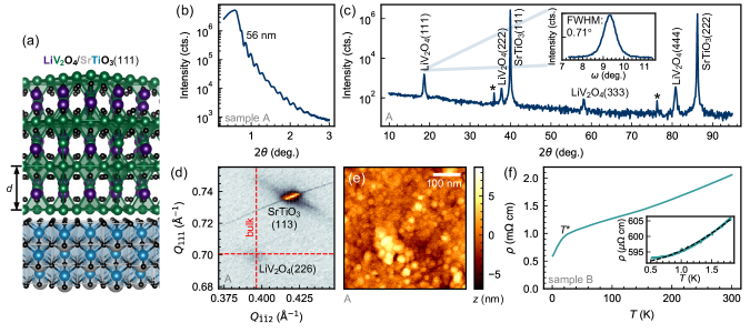
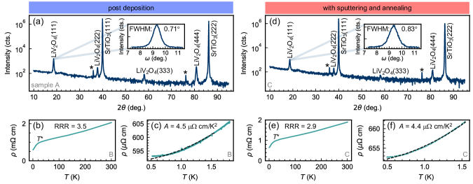
Figures 1(a)–1(d) present x-ray diffraction of a LiV2O4 film deposited on insulating SrTiO3(111) (sample A). We estimate the film thickness to be 56 nm, based on Kiessig oscillations in x-ray reflectivity measurements at grazing angles [Fig. 1(b)]. In the - scan [Fig. 1(c)], we observe all the allowed Bragg reflections associated with the (111) planes of LiV2O4, confirming that the film grew epitaxially with a well-defined orientation. We extract an interplane spacing of 4.756 Å, consistent with that of single crystals of LiV2O4, (Ref. Chmaissem et al. (1997)). Reciprocal space mapping around the LiV2O4(226) peak [Fig. 1(d)] also reveals bulk-like values for the in-plane lattice parameter. Given the large lattice mismatch between bulk LiV2O4 and SrTiO3, , we would expect a relaxed, dislocated growth of LiV2O4 on SrTiO3. The relaxed growth may be responsible for the larger out-of-plane mosaicity of LiV2O4 films on SrTiO3(111) compared to those on MgAl2O4(111) and MgO(001), which have lattice constants of and and smaller lattice mismatches to LiV2O4, and , respectively. The larger out-of-plane mosaicity of the LiV2O4 films on SrTiO3(111) is evidenced in the full-width half-maximum (FWHM) of the rocking curve, which is 0.71∘ as seen in the inset of Fig. 1(c), but 0.06∘ for films on both MgAl2O4(111) Yajima et al. (2021) and MgO(001) Niemann et al. . Our films are metallic, as evidenced by transport measurements (Fig. 1(f); sample B). The resistivity exhibits the same qualitative behavior as in bulk single crystals Urano et al. (2000): a characteristic downturn at 20 K and a functional form , = 4.5 cm/K2, around 1.8 K (Fig. 1(f) inset). The residual resistivity ratio of 3.5 is nearly identical to that of LiV2O4/MgAl2O4(111) films Yajima et al. (2021), in spite of the large mosaicity, but lower than the value of 11 in LiV2O4/SrTiO3(001) films Niemann et al. .
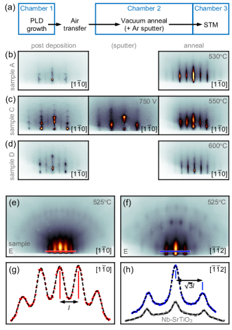
Having confirmed that our thin films possess the desired LiV2O4 phase, we turn to STM measurements. The exposure of oxide thin films to air contaminates the surface and hampers atomically resolved STM. In particular, single crystals of LiV2O4 are known to be sensitive to air and moisture Matsushita, Ueda, and Ueda (2005). Since we could not avoid atmospheric exposure when transferring our films from the PLD chamber to the STM system, we needed a means to recover pristine surfaces [Fig. 2(a)]. Furthermore, AFM reveals that as-grown films often show a granular topography [Fig. 1(e)]. To improve the surface quality, we performed Ar sputtering with moderate intensity (750 V, 10-3 mbar Ar partial pressure), followed by annealing at 550∘C in UHV for a few hours (sample C). We could also obtain suitable surfaces with just UHV annealing at 530–600∘C, without sputtering (samples A, D, and E). Later STM images reveal no systematic differences between the two methods. As seen in Figs. 2(b)–2(d), the RHEED patterns of as-grown films are somewhat spotty, indicating a rougher, three-dimensional (3D) surface, but become brighter with sharper streaks after sputtering and annealing, indicating a smoother, 2D surface. The diffraction patterns are nearly identical to that of LiTi2O4(111) films Okada et al. (2017); Ohsawa et al. (2020) and show clear in-plane orientation with streaks along [2] spaced times farther apart than streaks along [10], as expected for a hexagonal Bravais lattice [Figs. 2(e)–2(h)]. Comparing with the RHEED pattern obtained from a bare SrTiO3(111) substrate [Fig. 2(h)], we extract the epitaxial relationship LiV2O4[2] SrTiO3[2] and a 4.9% difference in the in-plane lattice constants, close to the 5.2% mismatch of their bulk values. These results from surface-sensitive RHEED are fully consistent with those from bulk-sensitive XRD in Fig. 1. (Figures S4 and S5 in the supplementary material present XRD and transport measurements of a film after sputtering and annealing, confirming the target LiV2O4(111) phase with heavy fermion behavior, as well as an estimation of Li stoichiometry from the lattice constant.)
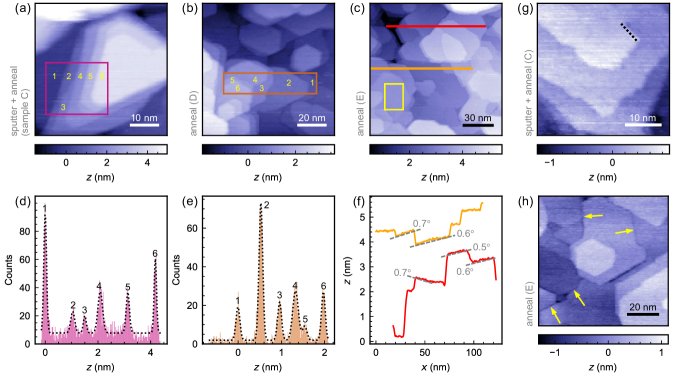
Figures 3(a)–3(c) show room-temperature STM images of LiV2O4(111) films after annealing in UHV with or without sputtering, demonstrating clear step-and-terrace structure, in contrast to the granular morphology seen immediately after PLD [Fig. 1(e)]. We consistently observed a landscape of islands with atomically smooth tops. In Fig. 3(c), the root-mean-square roughness is 1.0 nm over a 140140 nm field of view with many islands, but 37 pm within a single island (yellow box). The islands have a typical lateral diameter of 20–30 nm and adopt compact shapes, including triangular [Fig. 3(a)], hexagonal [Figs. 3(b) and 3(c)], and round [Figs. 3(b) and 3(c)] shapes. These compact islands, as opposed to dendritic or fractal islands, indicate that the film adatoms have sufficient mobility to diffuse along the perimeter of the islands to achieve shapes that are more thermodynamically favored Oura et al. (2003). Images of films with submonolayer coverage reveal that the formation of LiV2O4 islands begins at the SrTiO3(111) interface (see Fig. S6 in the supplementary material). The growth mode of LiV2O4 on SrTiO3(111) is classified as Volmer-Weber, where the growth of islands starts at the substrate, as opposed to Stranski-Krastanov, where the film initially grows uniformly with layer-by-layer coverage, then switches to island growth beyond a critical thickness. Volmer-Weber growth mode is often facilitated by a large lattice mismatch between film and substrate, as is the case here.
We take a closer look at the STM topographies by analyzing the island heights. In a few cases, such as in Fig. 3(a), where the islands on top of each other have the same shape with parallel step edges, we found the step heights to be regular and close to integer multiples of the lattice spacing along [111]. The histogram in Fig. 3(d) shows five terraces with a repeating height difference of 10.4 Å, which is within 9% of 2, and a sixth terrace with a height difference 4.6 Å, which is within 3% of . In many other cases, such as in Fig. 3(b), where the islands on top of each other have different shapes, the step heights are often irregular. The height differences between the successive terraces numbered in Fig. 3(b) are 5.3, 4.3, 3.7, 2.1, and 4.3 Å [Fig. 3(e)]. These irregular step heights could imply that the islands have different surface terminations, as there are six distinct atomic layers along the [111] direction of LiV2O4 [Fig. 1(a)]. Alternatively, there could be stacking faults beneath the surface that shift the heights of the terraces by less than one full unit cell Goswami et al. (2007). Spinel compounds are indeed known to host dislocations and antiphase boundaries that produce fractional shifts of the unit cell Yanina and Barry Carter (2002); Nedelkoski et al. (2017). In addition to the irregular terrace heights, we observed terraces that are tilted relative to the (111) plane. The height profiles in Fig. 3(f) reveal that some of the island tops are inclined, for example, by about 0.5–0.7∘. This out-of-plane mosaicity may correspond to the sizeable FWHM of the (111) rocking curve [inset of Fig. 1(c)].
We observed two further, distinct kinds of structural defects with STM: screw dislocations and trenches. Figure 3(g) shows an example of an island with a screw dislocation (dotted line). The implication of a screw dislocation is that the island grows via spiral growth Goswami et al. (2007). In spiral growth, adatoms nucleate at the exposed edge of the screw dislocation and cause the island to grow by winding. In contrast, the many other islands in Figs. 3(a)–3(c) with flat tops grow via 2D nucleation, wherein each layer is successively formed on top of another Redinger et al. (2008). From the prevalence of islands with flat tops over islands with screw dislocations in our images, we conclude that 2D nucleation plays a greater role than that of spiral growth in our films, but both growth modes are present. Figure 3(h) shows examples of a different structural defect, that is, narrow trenches at the boundaries between islands. The implication of trenches is that the neighboring islands have failed to coalesce, likely because the edge atoms are out of phase. These boundaries make it difficult for the film to form one continuous domain and perpetuate island growth.
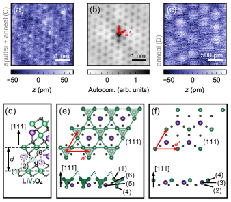
When the STM tip was brought closer to the surface of the islands, we observed a hexagonal atomic lattice [Figs. 4(a) and 4(c)]. The lattice constant, as extracted from an autocorrelation [Fig. 4(b)], is Å, close to and within the instrument - calibration error of the bulk value for the LiV2O4(111)-11 surface, Å. Six atomic (111) terminations are possible, as labeled in Fig. 4(d): (1)-V, (2)-O, (3)-Li, (4)-V, (5)-Li, and (6)-O. We hypothesize that the bright lobes in the STM image arise from V atoms either in the kagome (1)-V [Fig. 4(e)] or hexagonal (4)-V [Fig. 4(f)] layers. First-principles calculations consistently find that the V orbitals dominate near the Fermi energy Eyert et al. (1999); Matsuno, Fujimori, and Mattheiss (1999). Therefore, even if the surface were terminated by Li or O atoms, they could be invisible to STM. To further distinguish between the kagome (1)-V and hexagonal (4)-V terminations, however, is difficult. In the bulk spinel crystal, every V tetrahedron is equivalent. At a kagome (1)-V surface, this degeneracy is broken by a missing V atom in every second tetrahedron at the surface [dashed lines in Fig. 4(e)]. If the charge density becomes concentrated at the V tetrahedra that remain intact [shaded regions in Fig. 4(e)], then STM could also image a hexagonal lattice for the kagome (1)-V surface, similar to that of the hexagonal (4)-V surface.
The stabilization of atomically flat LiV2O4(111) surfaces is a nontrivial observation whose mechanism requires further study. According to Tasker’s classification Tasker (1979), the six possible atomic terminations in the (111) plane are all type III, meaning that a net dipole moment perpendicular to the surface exists. The resulting electrostatic potential would diverge, unless the surface atomic or electronic structure deviates from the bulk. Since we observe a LiV2O4(111)-11 termination, we exclude a surface reconstruction that enlarges the unit cell in the in-plane directions, as often witnessed in the perovskite oxides, or [001]- and [110]-oriented spinels Chang et al. (2016); Walls et al. (2016). Past studies of Fe3O4(111) and Co3O4(111) inferred that surface polarity could be compensated on a 11 termination simply by an inward relaxation of the surface Fe3+/Co2+ ions and a corresponding shortening of the Fe-O/Co-O bonds, which indicates increased covalency Ritter and Weiss (1999); Meyer et al. (2008). Alternatively, Li deficiency Azuma et al. (2013) (see Fig. S5 in the supplementary material) or an exchange of the surface Li and V positions (inverse spinel structure), as proposed for LiMn2O4(111) Kim, Aykol, and Wolverton (2015), may also occur to counteract surface polarity. It is tempting to infer that these mechanisms to stabilize the polar (111) surface could also be connected to the irregular step heights observed in Fig. 3.
In summary, we have demonstrated that STM topographic imaging with atomic resolution is possible with epitaxial LiV2O4(111) films. An enabling step is a vacuum annealing procedure with optional Ar sputtering that cleanses and smoothens the surface. This simple technique circumvents the need for in-situ transfer of films, thus opening the door to applying a wide range of surface-sensitive spectroscopic probes on LiV2O4. In particular, both low-temperature scanning tunneling spectroscopy and photoemission spectroscopy will be crucial in elucidating the nature of the heavy fermion phase. From our room-temperature STM measurements of LiV2O4, we could also glean clues about film-growth mechanisms. As a future work, it would be interesting to investigate whether uniform, layer-by-layer growth of LiV2O4 with fewer structural defects is possible by tuning growth and annealing conditions, choosing a substrate with a smaller lattice mismatch, or growing in the [001] or [110] orientations, or whether the island growth observed in this work is inevitable in the PLD of LiV2O4 films.
Supplementary Material
See supplementary material for additional information on growth and surface preparation, STM calibration, film properties after sputtering and annealing, estimation of Li stoichiometry, and Volmer-Weber growth mode of LiV2O4 on SrTiO3(111).
Acknowledgements.
We thank B. Stuhlhofer, G. Cristiani, K. Pflaum, M. Dueller, S. Prill-Diemer, H. Nakamura, K. Küster, and U. Starke for technical support and use of facilities. D.H. acknowledges support from a Humboldt Research Fellowship for Postdoctoral Researchers.References
- Kondo et al. (1997) S. Kondo, D. C. Johnston, C. A. Swenson, F. Borsa, A. V. Mahajan, L. L. Miller, T. Gu, A. I. Goldman, M. B. Maple, D. A. Gajewski, E. J. Freeman, N. R. Dilley, R. P. Dickey, J. Merrin, K. Kojima, G. M. Luke, Y. J. Uemura, O. Chmaissem, and J. D. Jorgensen, Phys. Rev. Lett. 78, 3729 (1997).
- Urano et al. (2000) C. Urano, M. Nohara, S. Kondo, F. Sakai, H. Takagi, T. Shiraki, and T. Okubo, Phys. Rev. Lett. 85, 1052 (2000).
- Kessler and Sienko (1971) H. Kessler and M. J. Sienko, J. Chem. Phys. 55, 5414 (1971).
- Anderson (1956) P. W. Anderson, Phys. Rev. 102, 1008 (1956).
- Verwey (1939) E. J. W. Verwey, Nature 144, 327 (1939).
- Matsuno et al. (2001) K. Matsuno, T. Katsufuji, S. Mori, Y. Moritomo, A. Machida, E. Nishibori, M. Takata, M. Sakata, N. Yamamoto, and H. Takagi, J. Phys. Soc. Japan 70, 1456 (2001).
- Yamada and Tanaka (1995) A. Yamada and M. Tanaka, Mater. Res. Bull. 30, 715 (1995).
- Okamoto et al. (2008) Y. Okamoto, S. Niitaka, M. Uchida, T. Waki, M. Takigawa, Y. Nakatsu, A. Sekiyama, S. Suga, R. Arita, and H. Takagi, Phys. Rev. Lett. 101, 086404 (2008).
- Browne et al. (2018) A. J. Browne, C. Lithgow, S. A. J. Kimber, and J. P. Attfield, Inorg. Chem. 57, 2815 (2018).
- Chmaissem et al. (1997) O. Chmaissem, J. D. Jorgensen, S. Kondo, and D. C. Johnston, Phys. Rev. Lett. 79, 4866 (1997).
- Matsuno, Fujimori, and Mattheiss (1999) J. Matsuno, A. Fujimori, and L. F. Mattheiss, Phys. Rev. B 60, 1607 (1999).
- Shimoyamada et al. (2006) A. Shimoyamada, S. Tsuda, K. Ishizaka, T. Kiss, T. Shimojima, T. Togashi, S. Watanabe, C. Q. Zhang, C. T. Chen, Y. Matsushita, H. Ueda, Y. Ueda, and S. Shin, Phys. Rev. Lett. 96, 026403 (2006).
- Jönsson et al. (2007) P. E. Jönsson, K. Takenaka, S. Niitaka, T. Sasagawa, S. Sugai, and H. Takagi, Phys. Rev. Lett. 99, 167402 (2007).
- Shimizu et al. (2012) Y. Shimizu, H. Takeda, M. Tanaka, M. Itoh, S. Niitaka, and H. Takagi, Nat. Commun. 3, 981 (2012).
- Browne et al. (2020) A. J. Browne, E. J. Pace, G. Garbarino, and J. P. Attfield, Phys. Rev. Mater. 4, 015002 (2020).
- Anisimov et al. (1999) V. I. Anisimov, M. A. Korotin, M. Zölfl, T. Pruschke, K. Le Hur, and T. M. Rice, Phys. Rev. Lett. 83, 364 (1999).
- Fulde et al. (2001) P. Fulde, A. N. Yaresko, A. A. Zvyagin, and Y. Grin, EPL 54, 779 (2001).
- Burdin, Grempel, and Georges (2002) S. Burdin, D. R. Grempel, and A. Georges, Phys. Rev. B 66, 045111 (2002).
- Fujimoto (2002) S. Fujimoto, Phys. Rev. B 65, 155108 (2002).
- Hopkinson and Coleman (2002) J. Hopkinson and P. Coleman, Phys. Rev. Lett. 89, 267201 (2002).
- Yamashita and Ueda (2003) Y. Yamashita and K. Ueda, Phys. Rev. B 67, 195107 (2003).
- Arita et al. (2007) R. Arita, K. Held, A. V. Lukoyanov, and V. I. Anisimov, Phys. Rev. Lett. 98, 166402 (2007).
- Hattori and Tsunetsugu (2009) K. Hattori and H. Tsunetsugu, Phys. Rev. B 79, 035115 (2009).
- Yajima et al. (2021) T. Yajima, T. Soma, K. Yoshimatsu, N. Kurita, M. Watanabe, and A. Ohtomo, Phys. Rev. B 104, 245104 (2021).
- (25) U. Niemann, Y. M. Wu, R. Oka, D. Hirai, Y. Wang, Y. E. Suyolcu, M. Kim, P. A. van Aken, and H. Takagi, arXiv:2206.11585 .
- Lu et al. (2019) Y. Lu, X. Zeng, J. Wang, L. Yang, S. Hu, C. Jia, H. Zhao, D. Yin, X. Ge, and X. Xi, Adv. Mater. Interfaces 6, 1901368 (2019).
- Das et al. (2007) S. Das, X. Zong, A. Niazi, A. Ellern, J. Q. Yan, and D. C. Johnston, Phys. Rev. B 76, 054418 (2007).
- Ritter and Weiss (1999) M. Ritter and W. Weiss, Surf. Sci. 432, 81 (1999).
- Meyer et al. (2008) W. Meyer, K. Biedermann, M. Gubo, L. Hammer, and K. Heinz, J. Phys.: Condens. Matter 20, 265011 (2008).
- Okada et al. (2017) Y. Okada, Y. Ando, R. Shimizu, E. Minamitani, S. Shiraki, S. Watanabe, and T. Hitosugi, Nature Commun. 8, 15975 (2017).
- Kitta et al. (2014) M. Kitta, T. Matsuda, Y. Maeda, T. Akita, S. Tanaka, Y. Kido, and M. Kohyama, Surf. Sci. 619, 5 (2014).
- Mishra and Thomas (1977) R. K. Mishra and G. Thomas, J. Appl. Phys. 48, 4576 (1977).
- Wen et al. (2020) F. Wen, X. Liu, M. Kareev, T.-C. Wu, M. Terilli, J. Chakhalian, P. Shafer, and E. Arenholz, Phys. Rev. B 102, 165426 (2020).
- Matsushita, Ueda, and Ueda (2005) Y. Matsushita, H. Ueda, and Y. Ueda, Nat. Mater. 4, 845 (2005).
- Ohsawa et al. (2020) T. Ohsawa, N. Yamada, A. Kumatani, Y. Takagi, T. Suzuki, R. Shimizu, S. Shiraki, T. Nojima, and T. Hitosugi, ACS Appl. Electron. Mater. 2, 517 (2020).
- Oura et al. (2003) K. Oura, V. Lifshits, A. Saranin, A. Zotov, and M. Katayama, Surface Science: An Introduction (Springer Berlin Heidelberg, 2003).
- Goswami et al. (2007) D. Goswami, K. Bhattacharjee, B. Satpati, S. Roy, P. Satyam, and B. Dev, Surf. Sci. 601, 603 (2007).
- Yanina and Barry Carter (2002) S. V. Yanina and C. Barry Carter, Surf. Sci. 511, 133 (2002).
- Nedelkoski et al. (2017) Z. Nedelkoski, D. Kepaptsoglou, L. Lari, T. Wen, R. A. Booth, S. D. Oberdick, P. L. Galindo, Q. M. Ramasse, R. F. L. Evans, S. Majetich, and V. K. Lazarov, Sci. Rep. 7, 45997 (2017).
- Redinger et al. (2008) A. Redinger, O. Ricken, P. Kuhn, A. Rätz, A. Voigt, J. Krug, and T. Michely, Phys. Rev. Lett. 100, 035506 (2008).
- Eyert et al. (1999) V. Eyert, K.-H. Höck, S. Horn, A. Loidl, and P. S. Riseborough, EPL 46, 762 (1999).
- Tasker (1979) P. W. Tasker, J. Phys. C: Solid State Phys. 12, 4977 (1979).
- Chang et al. (2016) C. F. Chang, Z. Hu, S. Klein, X. H. Liu, R. Sutarto, A. Tanaka, J. C. Cezar, N. B. Brookes, H.-J. Lin, H. H. Hsieh, C. T. Chen, A. D. Rata, and L. H. Tjeng, Phys. Rev. X 6, 041011 (2016).
- Walls et al. (2016) B. Walls, O. Lübben, K. Palotás, K. Fleischer, K. Walshe, and I. V. Shvets, Phys. Rev. B 94, 165424 (2016).
- Azuma et al. (2013) K. Azuma, C. Dover, D. C. Grinter, R. Grau-Crespo, N. Almora-Barrios, G. Thornton, T. Oda, and S. Tanaka, J. Phys. Chem. C 117, 5126 (2013).
- Kim, Aykol, and Wolverton (2015) S. Kim, M. Aykol, and C. Wolverton, Phys. Rev. B 92, 115411 (2015).
- (47) SpringerMaterials database.
- Fujita et al. (1997) D. Fujita, K. Amemiya, T. Yakabe, H. Nejoh, T. Sato, and M. Iwatsuki, Phys. Rev. Lett. 78, 3904 (1997).
- de Picciotto and Thackeray (1985) L. de Picciotto and M. Thackeray, Mater. Res. Bull. 20, 1409 (1985).
Supplementary Material
Growth parameters and surface preparation
The growth parameters and surface preparation of the LiV2O4(111) films reported in this work are given in Tables S1 and S2.
| Sample | Substrate | Deposition | Laser energy | Laser fluence | Pulses | Repetition | Figures |
|---|---|---|---|---|---|---|---|
| temperature (∘C) | at output (mJ) | (J/cm2) | rate (Hz) | ||||
| A | SrTiO3(111) | 660 | 720 | 1.5 | 1500 | 5 | 1(b)–1(e), 2(b), S4(a), S5 |
| B | SrTiO3(111) | 660 | 790 | 1.7 | 1500 | 5 | 1(f), S4(b), S4(c) |
| C | SrTiO3(111) | 660 | 720 | 1.5 | 1500 | 5 | 2(c), 3(a), 3(d), 3(g), 4(a), 4(b) |
| S4(d)–S4(f), S5 | |||||||
| D | Nb-SrTiO3(111) | 520 | 780 | 1.6 | 1500 | 5 | 2(d), 3(b), 3(e), 4(c), S5 |
| E | Nb-SrTiO3(111) | 580 | 800 | 1.7 | 1500 | 5 | 2(e)–2(h), 3(c), 3(f), 3(h), S5 |
| F | Nb-SrTiO3(111) | 520 | 780 | 1.6 | 1000 | 5 | S1 |
| G | SrTiO3(111) | 660 | 720 | 1.5 | 1000 | 5 | S5 |
| H | SrTiO3(111) | 660 | 810 | 1.7 | 1500 | 5 | S5 |
| I | Nb-SrTiO3(111) | 580 | 800 | 1.7 | 1500 | 5 | S5 |
| Sample | Procedure |
|---|---|
| A | Anneal up to 530∘C |
| C | Sputter up to 750 V in 10-3 mbar Ar partial pressure; anneal up to 550∘C |
| D | Anneal up to 600∘C |
| E | Anneal up to 600∘C |
| F | Sputter up to 750 V in 10-3 mbar Ar partial pressure; anneal up to 550∘C |
Additional sample
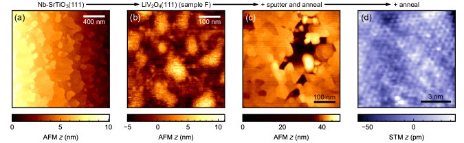
Figure S1 presents AFM and STM images of an additional LiV2O4(111) film (sample F) at four different stages: (a) bare substrate, (b) after PLD, (c) after sputtering and annealing, and (d) after additional annealing. As mentioned in the main text, we pretreated the SrTiO3(111) substrates by heating them up to 1000∘C in atmosphere for several hours, in order to obtain flat terraces [Fig. S1(a)]. The LiV2O4 film after PLD has a granular surface morphology, as seen in Fig. S1(b). After sputtering and annealing, as previously described, AFM reveals triangular, hexagonal and round islands with flat tops [Fig. S1(c)]. STM resolves a hexagonal atomic lattice [Fig. S1(d)].
Growth window
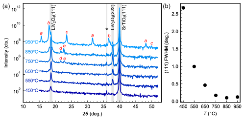
We investigated the deposition of LiV2O4(111) films at substrate temperatures ranging from 450 to 950∘C. As seen in Fig. S2(a), at the lowest temperature of 450∘C, the amplitude of the LiV2O4(111) Bragg reflection in XRD is weak, and the LiV2O4(222) reflection is not visible. As we increased the temperature, the amplitudes of both reflections increased and reached a maximum at 750–850∘C. However, impurity peaks are also visible starting around 750∘C. At 950∘C, it is clear that LiV2O4 is no longer the dominant phase in the film. The impurity phases are identified as various vanadates in Table S3, which suggests a loss of Li at temperatures above 750∘C.
According to Fig. S2(b), the LiV2O4 phase has the best crystallinity at 850∘C, with the lowest FWHM of the (111) Bragg reflection (0.1∘). However, the film is no longer phase pure. For the measurements presented in the main text, we have restricted the growth and vacuum annealing temperatures to the safer ranges of 520–660∘C and 500–600∘C, respectively. The slight difference in temperature ranges has to do with the temperature calibration of different systems, as well as some differences in heating of insulating SrTiO3 and conducting Nb-SrTiO3.
| Label | 2 (∘) | Possible identity of reflections | 2 (∘) | Dataset ID |
|---|---|---|---|---|
| 15.67, 31.59, 48.17 | V2O5(020), V2O5(040), V2O5(060) | 15.37, 31.03, 47.30 | sd-1500170 | |
| VO2(B)(200), VO2(B)(400), VO2(B)(600) | 15.36, 31.00, 47.27 | sd-1614307 | ||
| 18.08, 36.59 | VO2(100), VO2(200) | 18.29, 37.06 | sd-0455502 | |
| 23.55, 49.93 | VO2(B)(201), VO2(B)(402) | 23.96, 49.06 | sd-1614307 | |
| 21.67 | V3O7(204) | 21.78 | sd-0308766 | |
| V3O5(011) | 22.18 | sd-1724204 | ||
| 22.80 | – | – | – |
Calibration of STM height
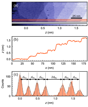
To ensure that the observation of irregular step heights in LiV2O4 films in Fig. 3 of the main text does not arise from an instrument artifact, we present control measurements of Au(111) with regular step heights in Fig. S3. From the orange box in Fig. S3(a) spanning several Au terraces, we computed a -height histogram [Fig. S3(c)], which revealed peaks at regularly spaced intervals. We could fit the histogram with a sum of Gaussian functions whose peaks are spaced by or 2; i.e., the terrace heights are integer multiples of a single variable, . We then calibrated the STM height to match with its literature value of 0.24 nm Fujita et al. (1997).
Bulk properties after sputtering and annealing
Figure S4 presents a comparison of XRD and transport of LiV2O4 films deposited on insulating SrTiO3(111) at 660∘C, immediately after PLD [Figs. S4(a)–S4(c)] and after sputtering and annealing to produce surfaces suitable for STM [Figs. S4(d)–S4(f)]. For the sputtered and annealed film (sample C), we observed the same Bragg reflections associated with the (111) planes of LiV2O4 [Fig. S4(d)]. The resistivity exhibits metallic behavior with a downturn at K and -like behavior below 1.5 K [Figs. S4(e)–S4(f)]. The reduced amplitude of the Bragg reflections, larger full-width half-maximum of the LiV2O4(111) rocking curve, reduced residual resistivity ratio, and larger lattice constant (Fig. S5) could reflect some effects of the sputtering and annealing, but these differences lie within the variation of our samples.
Estimation of Li stoichiometry from lattice constant
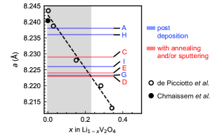
Due to the small atomic mass of Li and the thinness of our films, we were not able to accurately quantify the Li concentration with state-of-the-art energy-dispersive x-ray spectroscopy (EDX) instruments available to us. Indirectly, there is an empirical correlation between the Li deficiency in Li1-xV2O4 and the cubic lattice constant , based on powder sample studies de Picciotto and Thackeray (1985). As seen in Fig. S5, we extract the values for several films based on the () Bragg reflections and overlay them on the trend line of Li1-xV2O4. The films were grown throughout the course of our investigation using various growth and surface treatment conditions documented in Tables S1 and S2. We roughly estimate the Li deficiency in our films to be (gray shaded area in Fig. S5).
Volmer-Weber growth of LiV2O4 on SrTiO3(111)
From STM images of 50-nm-thick films (Fig. 3 of the main text), we cannot distinguish whether LiV2O4 grows on SrTiO3(111) in Volmer-Weber (VW) or Stranski-Krastanov (SK) mode. In the former, the deposited film forms islands starting at the substrate interface, whereas in the latter, the deposited film initially grows layer-by-layer at the substrate interface, before reverting to island growth past a critical thickness Oura et al. (2003). SK growth mode occurs when there is strong bonding between the film and substrate atoms.
To investigate the initial stages of growth, we deposited 15 pulses of LiV2O4 onto a SrTiO3(111) substrate held at 370∘C. (A different PLD chamber was used in this case, leading to slightly adjusted parameters.) Figure S6(a) shows a topography acquired ex situ via AFM. Rather than exhibiting a uniform coverage, the film is clustered into triangular islands, indicating that the film adatoms were mobile and underwent significant diffusion at the given deposition conditions. Some islands are lodged at the step edges of the SrTiO3(111) substrate, but many others are also located in the middle of the terraces. The triangular islands are identically oriented, which agrees with the RHEED data (Fig. 2 of the main text) showing the thick films to have clear in-plane orientation. We conclude that LiV2O4 on SrTiO3(111) exhibits VW, not SK, growth mode.
Figure S6(b) shows a smaller 500500 nm field of view. The average heights of the islands range from 1.0 to 2.2 nm, corresponding roughly to 2–4. For the ten islands labeled in Fig. S6(b), the lateral areas range from 500 to 1100 nm2, which are comparable to the island sizes observed in Fig. 3 of the main text. Unlike the thick films, however, only triangular, not hexagonal, islands are observed here. It is possible that the longer deposition time of thicker films, or the vacuum annealing procedure preceding STM imaging of those films, promoted further adatom diffusion and compactification of triangular islands into hexagonal islands, which are thermodynamically more stable Oura et al. (2003).
Figure S6(c) shows an AFM adhesion map acquired simultaneously with topography in Fig. S6(b). The map shows chemical contrast in the form of a lower adhesion for LiV2O4 compared to SrTiO3. However, the measurement is also sensitive to geometry, as the SrTiO3 terrace edges also exhibit reduced adhesion compared to the rest of the terrace.