Combined electronic excitation and knock-on damage in monolayer MoS2
Abstract
Electron irradiation-induced damage is often the limiting factor in imaging materials prone to ionization or electronic excitations due to inelastic electron scattering. Quantifying the related processes at the atomic scale has only become possible with the advent of aberration-corrected (scanning) transmission electron microscopes and two-dimensional materials that allow imaging each lattice atom. While it has been shown for graphene that pure knock-on damage arising from elastic scattering is sufficient to describe the observed damage, the situation is more complicated with two-dimensional semiconducting materials such as MoS2. Here, we measure the displacement cross section for sulfur atoms in MoS2 with primary beam energies between 55 and 90 keV, and correlate the results with existing measurements and theoretical models. Our experimental data suggests that the displacement process can occur from the ground state, or with single or multiple excitations, all caused by the same impinging electron. The results bring light to reports in the recent literature, and add necessary experimental data for a comprehensive description of electron irradiation damage in a two-dimensional semiconducting material. Specifically, the results agree with a combined inelastic and elastic damage mechanism at intermediate energies, in addition to a pure elastic mechanism that dominates above 80 keV. When the inelastic contribution is assumed to arise through impact ionization, the associated excitation lifetime is on the order of picoseconds, on par with expected excitation lifetimes in MoS2, whereas it drops to some tens of femtoseconds when direct valence excitation is considered.
I Introduction
Although electron irradiation damage in (scanning) transmission electron microscopy [(S)TEM] has been investigated for decades egerton_radiation_2004 ; egerton_control_2013 , its detailed quantification only became possible with two-dimensional (2D) materials susi_quantifying_2019 that allow imaging all atoms in the structure with aberration-corrected haider_spherical-aberration-corrected_1998 ; krivanek_towards_1999 ; kabius_first_2009 instruments. Beyond chemical etching leuthner_scanning_2019 taking place due to non-ideal vacuum or sample contamination (which was recently shown not to be the case for MoS2 even up to pressures of mbar ahlgren_atomic-scale_2022 ), this damage is known to result from elastic and inelastic scattering of the imaging electrons from the material. During the elastic process, the electron scatters with a nucleus, transferring it a certain amount of kinetic energy, which causes a displacement if the material- and element-specific displacement energy threshold is exceeded. Such displacements dominate at higher electron energies, and have been studied for several 2D materials such as hexagonal boron nitride meyer_selective_2009 ; jin_fabrication_2009 ; kotakoski_electron_2010 , graphene meyer_accurate_2012 ; meyer_erratum_2013 ; susi_isotope_2016 , MoS2 komsa_two-dimensional_2012 ; kretschmer_formation_2020 and MoSe2 lehtinen_atomic_2015 . In contrast, inelastic scattering arises from the interaction of the beam electron with other degrees of freedom causing charging, ionization, electron excitations, or heating of the target, which can lead to weakening or breaking of bonds egerton_control_2013 .
It has been well established that purely elastic knock-on describes electron beam damage in pristine graphene, and that lattice vibrations must be taken into account for an accurate description at electron energies close to the otherwise sharp damage onset determined by the displacement energy threshold of the material meyer_accurate_2012 ; meyer_erratum_2013 ; susi_isotope_2016 ; chirita_three-dimensional_2022 . However, a similarly detailed description of the knock-on process is lacking for semiconducting or insulating 2D materials both due to the lack of experimental data and theoretical models. Nevertheless, it is clear that the simple elastic model that is sufficient for graphene can not comprehensively describe electron beam damage in an insulator such as hexagonal boron nitride kotakoski_electron_2010 . Until now, the role of the inelastic scattering has been approached indirectly for the semiconducting transition metal dichalcogenides (TMDs) MoS2 algara-siller_pristine_2013 and MoSe2 lehnert_electron_2017 by comparing damage with and without a protective graphene layer. Meanwhile, the ground state displacement threshold energies (corresponding to the elastic case) for several TMDs have also been estimated through first-principles atomistic simulations komsa_two-dimensional_2012 ; yoshimura_first-principles_2018 . Only recently, the joint contribution of elastic and inelastic scattering to the damage in MoS2 has been directly considered by Kretschmer et al. combining experiments and simulations kretschmer_formation_2020 . Yoshimura et al. also recently developed a model combining density-functional theory (DFT) calculations and quantum electrodynamics (QED) to describe damage in non-conductive 2D materials yoshimura_quantum_2022 . However, the experimentally studied primary beam energy range has been limited to keV, precluding sulfur displacements from the electronic ground state, and no satisfactory agreement has been found between experimental results and a model with a direct physical interpretation.
In this work, we measure the displacement cross section in monolayer MoS2 at acceleration voltages of kV using aberration-corrected STEM imaging combined with a convolutional neural network-assisted analysis. Our results show a clear increase for the cross section values above 80 kV, which allows a direct comparison to theory including displacements also from the electronic ground state. We show that describing the inelastic contribution as impact ionization of the sulfur atom leads to a satisfactory agreement with the experimental data and a deexcitation time of up to picoseconds, in agreement with literature values korn_low-temperature_2011 ; lin_physical_2017 ; palummo_exciton_2015 . In contrast, describing it via valence excitation based on DFT calculations leads to a better agreement, but only with deexcitation lifetimes as short as some tens of femtoseconds, and only if the deexcitation is described as a collective process. Overall, the results presented here provide the first experimental data that allows the development of a comprehensive model for describing electron irradiation damage in a 2D semiconducting material, while also giving the first reliable indications of the relevant underlying physical phenomena.
II Results and Discussion
Monolayer MoS2 samples were grown by chemical vapor deposition (CVD), and transferred onto a TEM grid (Au grid with a Quantifoil carbon film) for STEM imaging (see Methods for details). Atomic resolution image series were recorded for acceleration voltages between 55 and 90 kV with a step size of 5 kV (ca. 100 series per voltage) to allow observing the displacement of sulfur atoms as a function of the electron dose. A typical recorded image series is shown in Fig. 1. The first row in this figure shows four consecutive unfiltered images of atomically resolved MoS2, where the lattice sites can be easily identified due to the -contrast pennycook_z-contrast_1989 of the STEM high angle annular dark field (HAADF) imaging mode (the contrast is approximately proportional to the atomic number krivanek_atom-by-atom_2010 ). A Gaussian blur was applied to the images in the second row, and in the third row those atomic positions that were taken into consideration during the following analysis are marked with circles. The first image (Fig. 1a) shows a completely intact hexagonal lattice structure of Mo atoms alternating with S sites (each having two S atoms on top of each other), indicated with purple and yellow circles, respectively. In the subsequent images, some of the sulfur sites exhibit reduced intensity (dotted orange circles), suggesting a missing sulfur atom at this position. Assuming that the number of any newly created vacancies is entirely stochastic and not dependent on the environment, a linear dependency is expected for the average number of new defects as a function of electron dose meyer_accurate_2012 ; meyer_erratum_2013 . We note that since all sulfur sites in the structure are equivalent, the field of view used in the measurement has no statistical influence on the uncertainty of the experimental results. However, this is only true as long as the local vacancy concentration remains low. For this reason, each experiment (image sequence) was ended when more than two sulfur vacancies appeared adjacent to one another as next nearest neighbors (as in Fig. 1d). Additionally, to avoid influence from contamination on the results, all image series with contamination were excluded from the analysis, as was also the area in each image closer to the edge than the projected Mo-S site distance. The histograms (last row in Fig. 1) show the sulfur site intensities of the corresponding image, that allow us to count the number of sulfur vacancies.
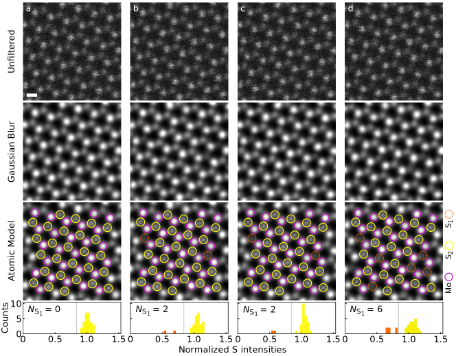
To assist defect recognition, a convolutional neural network (CNN) was used to identify the atomic positions for which the intensities are calculated. As indicated by the different colors, all intensities located below a certain threshold (shown with the grey line) are counted as vacancies. Due to variations in the intensity from one image series to the next, this threshold was set manually for each series. Despite the help of the CNN, this process is still estimated to lead to the largest uncertainty in the analysis, which was assessed by having the same data analyzed by two independant people. For the analysis, the number of defects present in the first frame is used as a reference, and only the change of the number of S vacancies during the experiment is used. Note that this number can also be negative when the identification of a site changes during the analysis due to changing intensity (either due to vacancy healing or due to inaccuracy in estimating the intensity due to noise). As the result, each image series yields an individual ratio for the number of created sulfur vacancies per image, obtained by fitting a linear regression to the data. Details on the CNN and the analysis method are described in the Methods section.
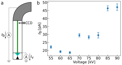
For each recorded image, we also store in the metadata the simultaneously measured current () at the virtual objective aperture (VOA) of the microscope. This corresponds to the part of the electron probe that is cut off by the aperture and never encounters the sample. To estimate the actual beam current , which is needed to calculate the electron dose per image, we carried out a set of calibration measurements, as schematically illustrated in Fig. 2a. In these measurements, instead of using a Faraday cup, as is typical with other instruments, was recorded as the current between the microscope ground and the drift tube for the electron energy loss spectrometer (without a sample), while simultaneously measuring . The dark current that was subtracted from was recorded by blocking the electron beam with the Ronchigram camera. Emission of the electron gun was altered by changing the extraction voltage during the measurement to establish the linear dependency of on to allow estimating the actual electron dose for each image. Note that the decay of the beam current of a cold field emission gun due to the absorption of gas molecules is known williams_transmission_2009 , but has no influence on our results, because the beam current is measured separately for each recorded image. We point out that it is typical to measure the beam current only sporadically and for short times, which based on our experiments can lead to significant errors in the estimated beam current. Therefore, we measure the beam current separately for each microscope alignment, and do the measurement for long enough (ca. 40 measurements and a total of up to several hours for each alignment) to ensure that its variation is correctly captured. The results from the beam current measurements are shown in Fig. 2b.
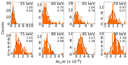
Combining the number of created vacancies from the analysis of the image series with the measured currents and the ratio allow us to calculate the average number of vacancies created per impinging electron for each image series. These data are summarised in histograms in Fig. 3. Although the knock-on process of a single atom is Poisson distributed over electron dose susi_siliconcarbon_2014 , we measure here the average from several such processes. According to the central limit theorem polya_uber_1920 , the measured expectation values collectively follow the normal distribution, as seen in Fig. 3. This allows us to calculate the knock-on cross section as , where is the mean of the normal distribution for and is the areal density of the sulfur site in MoS2 (i.e., the inverse of the unit cell area calculated with a lattice constant of Å ahmad_comparative_2014 ).
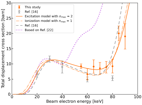
As was already pointed out, although for graphene elastic scattering is sufficient to describe the observed knock-on damage, this does not hold for MoS2. This is immediately apparent from the experimental data (Fig. 4), since for a purely elastic description, the cross section values should gradually increase almost exponentially within the acceleration voltage range studied here. In contrast, the results for MoS2 show a nearly constant value in the range of kV, and only start to increase above 80 kV. The purely elastic knock-on cross section can be described by the formalism of McKinley and Feshbach mckinley_coulomb_1948 modified to account for a target atom vibrating in the out-of-plane direction zobelli_electron_2007 , where
| (1) | |||
with being the displacement threshold energy (the lower boundary of energy that needs to be transferred to the atomic nucleus with mass and atomic number to cause a knock-on event). is the maximum kinetic energy that an electron with kinetic energy , elementary charge and electron rest mass can transfer to the nucleus moving at a velocity , is the vacuum permittivity, the speed of light in vacuum, the reduced Planck constant and is the velocity of the electron in units of . The velocity of the nucleus is determined via the material’s phonon dispersion, affecting and therefore as described in susi_isotope_2016 . The phonon dispersion of the material was calculated as described in the Methods.
Inelastic contributions to the process can be included via a probability , which can be constructed as the product of the probability of one electron impinging on the sample exciting electrons and the probability of these excitations to live long enough to contribute to the displacement process. Here, we discuss two different ways to take this into account. In the first one, where we write , we follow Kretschmer et al. kretschmer_formation_2020 , who assumed that the excitation can be described based on the ionization cross section according to Bethe bethe_zur_1930 . In the second one () we follow Yoshimura et al. yoshimura_quantum_2022 who calculated excitation probabilities directly from first principles. In both cases, we assume that the deexcitation takes place collectively (the system returns to ground state with a single deexcitation event), and follows Poisson statistics where the defining parameter is the excitation lifetime that leads to an exponentially decreasing probability for the excitation to exist long enough for the displacement to take place. In contrast, Kretschmer et al. kretschmer_formation_2020 replaced the deexcitation probability with an arbitrary efficiency factor, whereas Yoshimura et al. yoshimura_quantum_2022 considered the deexcitation of each of the excitations independently. The benefit of our approach over the one by Kretschmer et al. is that in our case all parameters of the model are physically motivated. In comparison, as will be discussed below, the assumption of independent deexcitation in the model proposed by Yoshimura et al. leads to a stark disagreement with our experimental data.
For completeness, the probabilities for an electronic excitation to occur and to exist long enough to influence the knock-on process as a function of the kinetic energy of the impinging electron become now
| (2) |
for excited states. Probability for the system to be in ground state is
| (3) |
is the time the atom needs to be displaced assuming that the impinging electron transferred an energy of exactly (we additionally assume, following Ref. kretschmer_formation_2020 the atom to be displaced when it has moved 4.5 Å from its original position). is the relativistic Bethe inelastic scattering cross section in a material with valence electrons as described in Ref. bui_electron_2023
| (4) | |||
where is the ionization energy, and and are constants relevant to the valence shell that we obtain by fitting the sum of the first and the second ionization cross section to the electron impact ionization data of sulfur tawara_total_1987 . The resulting fit parameters are and with ionization energies of eV and eV kelly_atomic_1982 . is the sum of all probabilities for all possible transitions from the valence into the conduction band, as described in Ref. yoshimura_quantum_2022 .
The total displacement cross section can then be written as
| (5) | |||
which was used to fit our experimental data. For fitting the models (the ionization model using and the excitation model using ), we also include the cross section values below 55 kV from Ref. kretschmer_formation_2020 since our data is limited to a voltage range of kV. However, we double the uncertainties given by Kretschmer et al. since they only reported uncertainties arising from the statistical sample size. Results of the fits are shown in Fig. 4.
| (eV) | (eV) | (eV) | (eV) | (fs) | (fs) | (fs) | |
|---|---|---|---|---|---|---|---|
| Ref. kretschmer_formation_2020 | 6.5t | 4.8t; 1.5f | 3.5t | ||||
| Ref. yoshimura_quantum_2022 | 6.92t | 5.04t | 3.16t | 1.28t | 81f | 81f | 81f |
| Ionization | 6.8 0.1 | 1.4 0.1 | |||||
| Excitation | 7.0 0.1 | 0.9 0.1 | 37 1 | ||||
| Excitation | 6.9 0.2 | 3.7 3.6 | 1.3 0.1 | 20 9 | 38 1 |
t Theoretically estimated value
f Value obtained from a fit
As can be seen from Fig. 4, both our models used here reasonably agree with the experimental data. As expected since they use the same inelastic scattering cross section model, the difference between the ionization model and the model by Kretschmer et al. kretschmer_formation_2020 is the smallest. For the displacement threshold from the ground state we obtain values between eV with all models, similar to the DFT values reported in Refs. komsa_two-dimensional_2012 ; yoshimura_first-principles_2018 ; yoshimura_quantum_2022 and somewhat above the value of Kretschmer et al. kretschmer_formation_2020 . In the case of the ionization model, the displacement threshold from the excited state (with ionized S) is eV, close to the value of Ref. kretschmer_formation_2020 , similarly obtained through a fit and mostly determined by their experimental data at the lowest acceleration voltages. The lifetime for the ionization resulting from this model is ps, which is similar to what was reported for excitons in MoS2 korn_low-temperature_2011 ; lin_physical_2017 ; palummo_exciton_2015 . We also point out that defects have been shown to extend the lifetime of excitons in TMDs by up to an order of magnitude liu_neutral_2019 . Adding multiple ionized states () did not result in an improved fit.
For the excitation model, the experimental data can be fitted with either one or two excited states, but we only show the plot for the latter case due to its better fit to the experimental data. With this model, the excited state displacement threshold energies become eV and eV, for single and double excitations, respectively. The very large uncertainty for the single excited state results from the relatively constant displacement cross section at intermediate energies, which allows fitting the data with different threshold energies varying the corresponding lifetime. The lifetimes for these excited states become fs and fs, which are the same order of magnitude as the 81 fs obtained in Ref. yoshimura_quantum_2022 , where all excitations were assumed independent and only was fitted to the experimental results of Ref. kretschmer_formation_2020 . It is worth noting that this time scale is longer than the lifetime of a core hole, but much shorter than the lifetimes of any other expected excitation. In essence, a lifetime that is too brief means that the used description of inelastic scattering gives a probability that is too high. Comparing these results suggests that the true inelastic contribution to the electron-beam damage cross section in MoS2 is similar to the probability for direct ionization, but smaller than the probability for valence excitation.
III Conclusions
In conclusion, our results confirm that inelastic scattering needs to be taken into account to accurately describe the knock-on process of S atoms from MoS2 under electron irradiation. Building on recent prior works kretschmer_formation_2020 ; yoshimura_quantum_2022 , we compare the experimental measurements to theoretical models, and show that the data can be qualitatively described by either assuming electron impact ionization of the sulfur atom or by assuming valence excitation of the material. The data is consistent with a sum of displacement cross sections for MoS2 at the ground state and one or more excited states with the lowest displacement threshold energy being ca. 1.3 eV (highest relevant excitation) and the highest, corresponding to the ground state, being ca. 6.9 eV. However, only with the impact ionization model the resulting lifetime becomes similar to excitation lifetimes reported in the literature (up to tens of picoseconds) korn_low-temperature_2011 ; lin_physical_2017 ; palummo_exciton_2015 , whereas the valence excitation leads to unexpectedly short lifetimes (tens of femtoseconds). Overall, the models presented here describe the experimentally measured displacement cross section in a 2D semiconducting material with only physically motivated parameters, which allows direct interpretation of the underlying physics opening the door to further theoretical work. Nevertheless, additional experimental data especially at lower electron energies are necessary to confirm that the cross section indeed increases gradually as suggested by the combination of inelastic and elastic scattering discussed here, rather than arising for example from chemical changes in the material under electronic excitation.
Methods
Sample preparation The MoS2 sample was grown on SiO2 via chemical vapor deposition (CVD) obrien_transition_2014 , and was afterwards transferred in air onto a gold transmission electron microscopy grid with a holey membrane of amorphous carbon (Quantifoil R 1.2/1.3 Au grid) with a method similar to that described in Ref. meyer_hydrocarbon_2008 . The sample was introduced to vacuum and baked overnight at ca. 150∘C before measurements were conducted. In between the measurements, the sample was stored in the CANVAS ultra-high vacuum system at the University of Vienna mangler_materials_2022 .
Scanning transmission electron microscopy Measurements were carried out with a Nion UltraSTEM 100, an aberration-corrected scanning transmission electron microscope with electron acceleration voltages in the range from 55 to 90 kV and a probe size of 1 Å. The instrument is equipped with a cold field emission gun, and images were recorded using high-angle annular dark field (HAADF) and medium-angle annular dark field (MAADF) detectors (for 60 kV only) with collection angles of mrad and mrad, respectively. The base pressure at the sample was below 10-9 mbar at all times. Imaging parameters were chosen to minimize the dose per frame while retaining enough signal to reliable recognize the atomic sites (dwell time of 3 s/px, flyback time of 120 s and images) resulting in a total frame time of 0.85 s with an additional 10 ms between the frames. The field of view for each image was 1.9 nm and the beam convergence angle was 30 mrad. Image series acquisition was stopped as soon as a small vacancy cluster (more than two missing S atoms at next-nearest neighboring lattice sites) was observed.
Phonon density of states calculation The phonon calculations were performed using the density functional perturbation theory (DFPT) baroni_phonons_2001 ; gonze_dynamical_1997 approach implemented in the ABINIT code gonze_abinit_2009 . First the lattice structure was optimized for both cell size and atomic positions up to an energy difference of Ha. We used a -point mesh of with an energy cut-off of 55 Ha. The local density approximation and the Troullier–Martins norm conserving pseudo-potentials troullier_efficient_1991 were used to describe the exchange correlation potential. For calculating the Hessian and dynamic matrix, the ground state wave functions were converged to Ha2 with a -point mesh of . Density of states was interpolated using the Gaussian method with a smearing value of Ha.
Data analysis The detection of sulfur vacancies was assisted by a CNN similar to the one described in Ref. trentino_atomic-level_2021 . The CNN calculates a heat map of probabilities of an atom being present at each pixel in each image, and converts this map into a set of atomic positions by locating peaks in the heat map. Later, a model image is created by overlapping the calculated atomic positions with the actual image and modelling the shape of the electron probe as a superposition of Gaussians. The optimization of the model is achieved by minimizing the intensity difference to the recorded image as described in Ref. postl_indirect_2022 . These intensities were then used to differentiate between the two different lattice sites, and to identify vacancies by setting an intensity threshold, labeling all sulfur lattice positions with a lowered intensity as vacancies. Image series containing any contamination or other disorder were discarded from the analysis. Similarly, only atoms at least one projected bond length away from the edge of the image were taken into account to rule out the influence of possible contamination, adatoms, and vacancy clusters located directly outside the field of view. The highest uncertainty of this analysis, apart from the subjective interpretation of the researcher, arose from the Gaussian fit in Fig. 3 (up to 10 %). To account for the uncertainty caused by the subjective interpretation of the researcher, the analysis for the datasets was done by two researchers independently. The total error was estimated by multiplying the uncertainty caused by the Gaussian fit with a factor of to contain both sources of uncertainty. All other uncertainties were deemed negligible in comparison to these errors.
Acknowledgments
We acknowledge funding from the Austrian Science Fund (FWF) through doctoral college Advanced Functional Materials–Hierarchical Design of Hybrid Systems (DOC 85), from the Vienna Doctoral School in Physics and from the European Research Council (ERC) under the European Union’s Horizon 2020 research and innovation programme Grant agreement No. 756277-ATMEN.
References
- (1) R. Egerton, P. Li, M. Malac, Radiation damage in the TEM and SEM, Micron 35 (6) (2004) 399–409. doi:10.1016/j.micron.2004.02.003.
- (2) R. Egerton, Control of radiation damage in the TEM, Ultramicroscopy 127 (2013) 100–108. doi:10.1016/j.ultramic.2012.07.006.
- (3) T. Susi, J. C. Meyer, J. Kotakoski, Quantifying transmission electron microscopy irradiation effects using two-dimensional materials, Nat Rev Phys 1 (6) (2019) 397–405. doi:10.1038/s42254-019-0058-y.
- (4) M. Haider, H. Rose, S. Uhlemann, E. Schwan, B. Kabius, K. Urban, A spherical-aberration-corrected 200kV transmission electron microscope, Ultramicroscopy 75 (1) (1998) 53–60. doi:10.1016/S0304-3991(98)00048-5.
- (5) O. L. Krivanek, N. Dellby, A. R. Lupini, Towards sub-Å electron beams, Ultramicroscopy 78 (1) (1999) 1–11. doi:10.1016/S0304-3991(99)00013-3.
- (6) B. Kabius, P. Hartel, M. Haider, H. Müller, S. Uhlemann, U. Loebau, J. Zach, H. Rose, First application of Cc-corrected imaging for high-resolution and energy-filtered TEM, Journal of Electron Microscopy 58 (3) (2009) 147–155. doi:10.1093/jmicro/dfp021.
- (7) G. T. Leuthner, S. Hummel, C. Mangler, T. J. Pennycook, T. Susi, J. C. Meyer, J. Kotakoski, Scanning transmission electron microscopy under controlled low-pressure atmospheres, Ultramicroscopy 203 (2019) 76–81. doi:10.1016/j.ultramic.2019.02.002.
- (8) E. H. Åhlgren, A. Markevich, S. Scharinger, B. Fickl, G. Zagler, F. Herterich, N. McEvoy, C. Mangler, J. Kotakoski, Atomic-Scale Oxygen-Mediated Etching of 2D MoS2 and MoTe2, Advanced Materials Interfaces 9 (32) (2022) 2200987. doi:10.1002/admi.202200987.
- (9) J. C. Meyer, A. Chuvilin, G. Algara-Siller, J. Biskupek, U. Kaiser, Selective Sputtering and Atomic Resolution Imaging of Atomically Thin Boron Nitride Membranes, Nano Lett. 9 (7) (2009) 2683–2689. doi:10.1021/nl9011497.
- (10) C. Jin, F. Lin, K. Suenaga, S. Iijima, Fabrication of a Freestanding Boron Nitride Single Layer and Its Defect Assignments, Phys. Rev. Lett. 102 (19) (2009) 195505. doi:10.1103/PhysRevLett.102.195505.
- (11) J. Kotakoski, C. H. Jin, O. Lehtinen, K. Suenaga, A. V. Krasheninnikov, Electron knock-on damage in hexagonal boron nitride monolayers, Phys. Rev. B 82 (11) (2010) 113404. doi:10.1103/PhysRevB.82.113404.
- (12) J. C. Meyer, F. Eder, S. Kurasch, V. Skakalova, J. Kotakoski, H. J. Park, S. Roth, A. Chuvilin, S. Eyhusen, G. Benner, A. V. Krasheninnikov, U. Kaiser, Accurate Measurement of Electron Beam Induced Displacement Cross Sections for Single-Layer Graphene, Phys. Rev. Lett. 108 (19) (2012) 196102. doi:10.1103/PhysRevLett.108.196102.
- (13) J. C. Meyer, F. Eder, S. Kurasch, V. Skakalova, J. Kotakoski, H. J. Park, S. Roth, A. Chuvilin, S. Eyhusen, G. Benner, A. V. Krasheninnikov, U. Kaiser, Erratum: Accurate Measurement of Electron Beam Induced Displacement Cross Sections for Single-Layer Graphene [Phys. Rev. Lett. 108, 196102 (2012)], Phys. Rev. Lett. 110 (23) (2013) 239902. doi:10.1103/PhysRevLett.110.239902.
- (14) T. Susi, C. Hofer, G. Argentero, G. T. Leuthner, T. J. Pennycook, C. Mangler, J. C. Meyer, J. Kotakoski, Isotope analysis in the transmission electron microscope, Nat Commun 7 (2016) 13040. doi:10.1038/ncomms13040.
- (15) H.-P. Komsa, J. Kotakoski, S. Kurasch, O. Lehtinen, U. Kaiser, A. V. Krasheninnikov, Two-Dimensional Transition Metal Dichalcogenides under Electron Irradiation: Defect Production and Doping, Phys. Rev. Lett. 109 (3) (2012) 035503. doi:10.1103/PhysRevLett.109.035503.
- (16) S. Kretschmer, T. Lehnert, U. Kaiser, A. V. Krasheninnikov, Formation of Defects in Two-Dimensional MoS in the Transmission Electron Microscope at Electron Energies below the Knock-on Threshold: The Role of Electronic Excitations, Nano Lett. 20 (4) (2020) 2865–2870. doi:10.1021/acs.nanolett.0c00670.
- (17) O. Lehtinen, H.-P. Komsa, A. Pulkin, M. B. Whitwick, M.-W. Chen, T. Lehnert, M. J. Mohn, O. V. Yazyev, A. Kis, U. Kaiser, A. V. Krasheninnikov, Atomic Scale Microstructure and Properties of Se-Deficient Two-Dimensional MoSe2, ACS Nano 9 (3) (2015) 3274–3283. doi:10.1021/acsnano.5b00410.
- (18) A. Chirita, A. Markevich, M. Tripathi, N. A. Pike, M. J. Verstraete, J. Kotakoski, T. Susi, Three-dimensional ab initio description of vibration-assisted electron knock-on displacements in graphene, Phys. Rev. B 105 (23) (2022) 235419. doi:10.1103/PhysRevB.105.235419.
- (19) G. Algara-Siller, S. Kurasch, M. Sedighi, O. Lehtinen, U. Kaiser, The pristine atomic structure of MoS2 monolayer protected from electron radiation damage by graphene, Appl. Phys. Lett. 103 (20) (2013) 203107. doi:10.1063/1.4830036.
- (20) T. Lehnert, O. Lehtinen, G. Algara–Siller, U. Kaiser, Electron radiation damage mechanisms in 2D MoSe2, Appl. Phys. Lett. 110 (3) (2017) 033106. doi:10.1063/1.4973809.
- (21) A. Yoshimura, M. Lamparski, N. Kharche, V. Meunier, First-principles simulation of local response in transition metal dichalcogenides under electron irradiation, Nanoscale 10 (5) (2018) 2388–2397. doi:10.1039/C7NR07024A.
- (22) A. Yoshimura, M. Lamparski, J. Giedt, D. Lingerfelt, J. Jakowski, P. Ganesh, T. Yu, B. G. Sumpter, V. Meunier, Quantum theory of electronic excitation and sputtering by transmission electron microscopy, Nanoscale (2022). doi:10.1039/D2NR01018F.
- (23) T. Korn, S. Heydrich, M. Hirmer, J. Schmutzler, C. Schüller, Low-temperature photocarrier dynamics in monolayer MoS , Appl. Phys. Lett. 99 (10) (2011) 102109. doi:10.1063/1.3636402.
- (24) W. Lin, Y. Shi, X. Yang, J. Li, E. Cao, X. Xu, T. Pullerits, W. Liang, M. Sun, Physical mechanism on exciton-plasmon coupling revealed by femtosecond pump-probe transient absorption spectroscopy, Materials Today Physics 3 (2017) 33–40. doi:10.1016/j.mtphys.2017.12.001.
- (25) M. Palummo, M. Bernardi, J. C. Grossman, Exciton Radiative Lifetimes in Two-Dimensional Transition Metal Dichalcogenides, Nano Lett. 15 (5) (2015) 2794–2800. doi:10.1021/nl503799t.
- (26) S. Pennycook, Z-contrast stem for materials science, Ultramicroscopy 30 (1-2) (1989) 58–69. doi:10.1016/0304-3991(89)90173-3.
- (27) O. L. Krivanek, M. F. Chisholm, V. Nicolosi, T. J. Pennycook, G. J. Corbin, N. Dellby, M. F. Murfitt, C. S. Own, Z. S. Szilagyi, M. P. Oxley, S. T. Pantelides, S. J. Pennycook, Atom-by-atom structural and chemical analysis by annular dark-field electron microscopy, Nature 464 (7288) (2010) 571–574. doi:10.1038/nature08879.
- (28) D. B. Williams, C. B. Carter, Transmission Electron Microscopy, Plenum Press, 2009.
- (29) T. Susi, J. Kotakoski, D. Kepaptsoglou, C. Mangler, T. C. Lovejoy, O. L. Krivanek, R. Zan, U. Bangert, P. Ayala, J. C. Meyer, Q. Ramasse, Silicon–Carbon Bond Inversions Driven by 60-keV Electrons in Graphene, Phys. Rev. Lett. 113 (11) (2014) 115501. doi:10.1103/PhysRevLett.113.115501.
- (30) G. Pólya, Über den zentralen Grenzwertsatz der Wahrscheinlichkeitsrechnung und das Momentenproblem, Math Z 8 (3) (1920) 171–181. doi:10.1007/BF01206525.
- (31) S. Ahmad, S. Mukherjee, A Comparative Study of Electronic Properties of Bulk MoS2 and Its Monolayer Using DFT Technique: Application of Mechanical Strain on MoS2 Monolayer, Graphene 03 (04) (2014) 52–59. doi:10.4236/graphene.2014.34008.
- (32) W. A. McKinley, H. Feshbach, The Coulomb Scattering of Relativistic Electrons by Nuclei, Phys. Rev. 74 (12) (1948) 1759–1763. doi:10.1103/PhysRev.74.1759.
- (33) A. Zobelli, A. Gloter, C. P. Ewels, G. Seifert, C. Colliex, Electron knock-on cross section of carbon and boron nitride nanotubes, Phys. Rev. B 75 (24) (2007) 245402. doi:10.1103/PhysRevB.75.245402.
- (34) H. Bethe, Zur Theorie des Durchgangs schneller Korpuskularstrahlen durch Materie, Annalen der Physik 397 (3) (1930) 325–400. doi:10.1002/andp.19303970303.
- (35) T. A. Bui, G. T. Leuthner, J. Madsen, M. R. A. Monazam, A. I. Chirita, A. Postl, C. Mangler, J. Kotakoski, T. Susi, in preparation (2023).
- (36) H. Tawara, T. Kato, Total and partial ionization cross sections of atoms and ions by electron impact, Atomic Data and Nuclear Data Tables 36 (2) (1987) 167–353. doi:10.1016/0092-640X(87)90014-3.
- (37) R. L. Kelly, Atomic and ionic spectrum lines below 2000A: hydrogen through argon, Tech. Rep. ORNL-5922, Oak Ridge National Lab., TN (USA) (Oct. 1982). doi:10.2172/6644558.
- (38) H. Liu, C. Wang, D. Liu, J. Luo, Neutral and defect-induced exciton annihilation in defective monolayer WS2, Nanoscale 11 (16) (2019) 7913–7920. doi:10.1039/C9NR00967A.
- (39) M. O’Brien, N. McEvoy, T. Hallam, H.-Y. Kim, N. C. Berner, D. Hanlon, K. Lee, J. N. Coleman, G. S. Duesberg, Transition Metal Dichalcogenide Growth via Close Proximity Precursor Supply, Sci Rep 4 (1) (2014) 7374. doi:10.1038/srep07374.
- (40) J. C. Meyer, C. O. Girit, M. F. Crommie, A. Zettl, Hydrocarbon lithography on graphene membranes, Appl. Phys. Lett. 92 (12) (2008) 123110. doi:10.1063/1.2901147.
- (41) C. Mangler, J. Meyer, A. Mittelberger, K. Mustonen, T. Susi, J. Kotakoski, A Materials Scientist’s CANVAS: A System for Controlled Alteration of Nanomaterials in Vacuum Down to the Atomic Scale, Microscopy and Microanalysis 28 (S1) (2022) 2940–2942. doi:10.1017/S1431927622011023.
- (42) S. Baroni, S. de Gironcoli, A. Dal Corso, P. Giannozzi, Phonons and related crystal properties from density-functional perturbation theory, Rev. Mod. Phys. 73 (2) (2001) 515–562. doi:10.1103/RevModPhys.73.515.
- (43) X. Gonze, C. Lee, Dynamical matrices, Born effective charges, dielectric permittivity tensors, and interatomic force constants from density-functional perturbation theory, Phys. Rev. B 55 (16) (1997) 10355–10368. doi:10.1103/PhysRevB.55.10355.
- (44) X. Gonze, B. Amadon, P. M. Anglade, J. M. Beuken, F. Bottin, P. Boulanger, F. Bruneval, D. Caliste, R. Caracas, M. Côté, T. Deutsch, L. Genovese, P. Ghosez, M. Giantomassi, S. Goedecker, D. R. Hamann, P. Hermet, F. Jollet, G. Jomard, S. Leroux, M. Mancini, S. Mazevet, M. J. T. Oliveira, G. Onida, Y. Pouillon, T. Rangel, G. M. Rignanese, D. Sangalli, R. Shaltaf, M. Torrent, M. J. Verstraete, G. Zerah, J. W. Zwanziger, ABINIT: First-principles approach to material and nanosystem properties, Computer Physics Communications 180 (12) (2009) 2582–2615. doi:10.1016/j.cpc.2009.07.007.
- (45) N. Troullier, J. L. Martins, Efficient pseudopotentials for plane-wave calculations, Phys. Rev. B 43 (3) (1991) 1993–2006. doi:10.1103/PhysRevB.43.1993.
- (46) A. Trentino, J. Madsen, A. Mittelberger, C. Mangler, T. Susi, K. Mustonen, J. Kotakoski, Atomic-Level Structural Engineering of Graphene on a Mesoscopic Scale, Nano Lett. 21 (12) (2021) 5179–5185. doi:10.1021/acs.nanolett.1c01214.
- (47) A. Postl, P. P. P. Hilgert, A. Markevich, J. Madsen, K. Mustonen, J. Kotakoski, T. Susi, Indirect measurement of the carbon adatom migration barrier on graphene, Carbon 196 (2022) 596–601. doi:10.1016/j.carbon.2022.05.039.