Integrated waveguide-based acousto-optic modulation with near-unity conversion efficiency
††journal: opticajournal††articletype: Research ArticleAcousto-optic modulation in piezoelectric materials offers the efficient method to bridge electrical and optical signals. It is widely used to control optical frequencies and intensities in modern optical systems including Q-switch lasers, ion traps, and optical tweezers. It is also critical for emerging applications such as quantum photonics and non-reciprocal optics. Acousto-optic devices have recently been demonstrated with promising performance on integrated platforms. However, the conversion efficiency of optical signals remains low in these integrated devices. This is attributed to the significant challenge in realizing large mode overlap, long interaction length, and high power robustness at the same time. Here, we develop acousto-optic devices with gallium nitride on sapphire substrate. The unique capability to confine both optical and acoustic fields in sub-wavelength scales without suspended structures allows efficient acousto-optic interactions over long distances under high driving power. This leads to the near-unity optical conversion efficiency with integrated acousto-optic modulators. With the unidirectional phase matching, we also demonstrate the non-reciprocal propagation of optical fields with isolation ratio above 10 dB. This work provides a robust and efficient acousto-optic platform, opening new opportunities for optical signal processing, quantum transduction, and non-magnetic optical isolation.
1 Introduction
Large-scale integration and device minimization are powerful methods to improve system functionality and efficiency. This is witnessed by the recent development of nonlinear optics in integrated photonic circuits [1, 2, 3, 4]. Compared with optical fields, acoustic fields have much lower propagation speed and stronger coupling with electric fields, thus providing complementary benefits for signal processing [5]. Therefore, tailored interactions between optical and acoustic fields in hybrid photonic-phononic circuits attract significant attentions recently with potential applications ranging from quantum transduction [6, 7, 8] and comb generation [9, 10] to photonic machine learning [11].
Acousto-optic modulation (AOM) plays a critical role in such hybrid circuits for signal conversion among different degrees of freedom. Intensive efforts have been devoted to the development of integrated acousto-optic modulators based on different piezoelectric materials including lithium niobate [12, 9, 13], aluminum nitride [14, 15, 16], gallium arsenide [17], and indium phosphire [18]. Efficient AOM requires the simultaneous confinement of optical and acoustic fields in sub-wavelength structures [13]. While optical confinement can be readily realized using materials with higher refractive index for waveguides, acoustic confinement is challenging as integrated photonic materials typically have acoustic velocities higher than substrates [19]. The lack of acoustic confinement leads to small coupling strengths between optical and acoustic fields due to the small mode overlapping. While the simultaneous confinement of optical and acoustic fields can be realized in suspended structures, the interaction length and power handling capability are limited due to the mechanical fragility [13]. The complex fabrication process also causes high acoustic propagation losses, which further deceases the interaction length. As a result, high optical conversion efficiency is still out of reach for integrated acousto-optic devices.
In this article, we overcome these challenges to realize near-unity conversion efficiencies with integrated acousto-optic modulators. This is achieved by developing the gallium nitride (GaN) on sapphire platform. The refractive index of GaN is significantly larger than sapphire [20]. More importantly, velocities of both transverse and longitudinal acoustic waves in GaN are remarkably lower than sapphire [19]. Therefore, we can realize sub-wavelength confinement of both optical and acoustic fields in GaN waveguides on sapphire substrates without suspended structures. Strong acousto-optic coupling can be realized over long interaction lengths under high driving power with minimal propagation losses, leading to the near-unity optical conversion efficiency.
2 Results
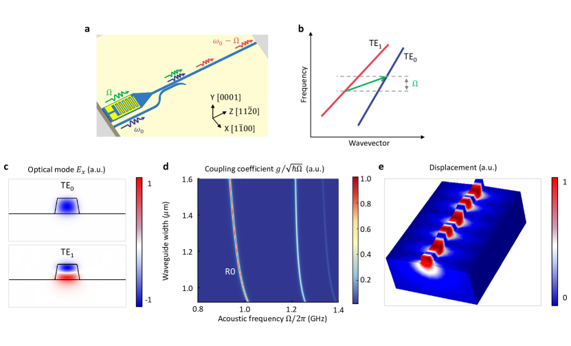
The integrated acousto-optic modulator is schematically depicted in Fig. 1a. Acoustic fields are launched by interdigital transducers (IDT) through the piezoelectric effect, and focused into the waveguide. Optical fields are launched through a separate waveguide, and transferred into the same waveguide with acoustic fields through a directional coupler. For co-propagating acoustic and optical fields, AOM can occur as both Stokes and anti-Stokes processes. Input optical fields at angular frequency are scattered by acoustic fields at angular frequency to generate the output optical field at and in the Stokes and anti-Stokes processes respectively. The corresponding phase matching conditions are and with , , and the acoustic, optical input, and optical output wavevectors respectively (Fig. 1b). We can switch between Stokes and anti-Stokes processes by interchanging the optical input and output modes [15]. Here, we use the fundamental and first-order transverse-electric (TE0 and TE1) modes for the input and output optical fields respectively (Fig. 1c). As the TE0 mode has a larger wave-vector (), the Stokes process dominates the acousto-optic modulation in our device. The conversion between TE0 and TE1 optical modes can be mediated by different acoustic modes. We perform numerical simulations to calculate the acousto-optic coupling coefficient [21]. Multiple acoustic modes can mediate efficient acousto-optic coupling between TE0 and TE1 modes as shown in Fig. 1d. We choose the fundamental Rayleigh (R0) acoustic mode, which shows the largest coupling strength. Moreover, with the significant out-of-plane displacement, the fundamental Rayleigh mode can be efficiently excited by IDTs on GaN (0001) plane (Fig. 1e) [22]. Due to the strong sub-wavelength confinement, the acousto-optic modulation process shows significant geometric dispersion. Therefore, the acoustic frequency can be tuned by the waveguide width. The waveguide width of our device is designed to be 1 m. Therefore, the phase matching condition can be satisfied near the acoustic frequency 1 GHz.
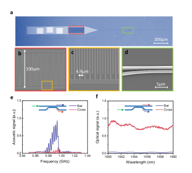
The device is fabricated with 1-m thick GaN template wafers grown on sapphire substrates using metal-organic chemical vapor deposition (Fig. 2a). Acousto-optic devices are patterned by the electron-beam lithography (EBL) using FOX-16 resist. After developing in TMAH, we etch the GaN layer with reactive ion etching using Cl2/BCl3/Ar gases. IDTs are defined with EBL in ploymethyl methacrylate (PMMA) resist, followed by Ti/Al/Au deposition and lift-off in acetone. The total waveguide length is mm to ensure efficient acousto-optic interaction. IDTs consist of a 5-nm titanium bottom layer, 100-nm aluminium middle layer, and 10-nm gold top layer. The IDT period is designed as 4.9 m to match the acoustic frequency around 1 GHz (Supplementary Section 1). The IDT aperture and electrode width are 100 m and 1.22 m respectively (Fig. 2b and c). The directional coupler consists of two parallel 800 nm wide waveguides with 400 nm gap (Fig. 2d). As acoustic and optical fields have different coupling strengths between the two waveguides, the same directional coupler structure can be designed to show different functions for acoustic and optical fields. Here, we set the directional coupler length at 250 m, in which case acoustic fields remain in the same waveguide and optical fields are completely transferred into the other waveguide (Supplementary Section 2).
We first use the vector network analyzer (VNA) to measure the acoustic transmission between IDT pairs directly connected by straight GaN waveguides with different lengths. The dependence of the acoustic transmission on the device length allows us to estimate the propagation loss of the fundamental Rayleigh mode, which is dB/mm (Supplementary Section 1). By extrapolating the acoustic transmission to zero device length, we can obtain the IDT power efficiency dB. With 50 periods, IDTs show a center frequency of 0.99 GHz and 3-dB bandwidth of 12 MHz. To verify the directional coupler performance, we fabricated test devices with four input/output ports connected all with IDTs for acoustic field characterization or all with optical couplers for optical field characterization (Fig. 2e and f). We only observe strong acoustic signal in the bar configuration of the directional coupler (Fig. 2e). The oscillation in the acoustic transmission spectrum is caused by the reflection between input and output IDTs. Extinction ratio above 10 dB between the bar and cross waveguides can be achieved. For optical fields, we only observe strong output in the cross configuration with average extinction ratio above 14 dB (Fig. 2f). This shows that optical fields and acoustic fields can be efficiently combined by the directional coupler.
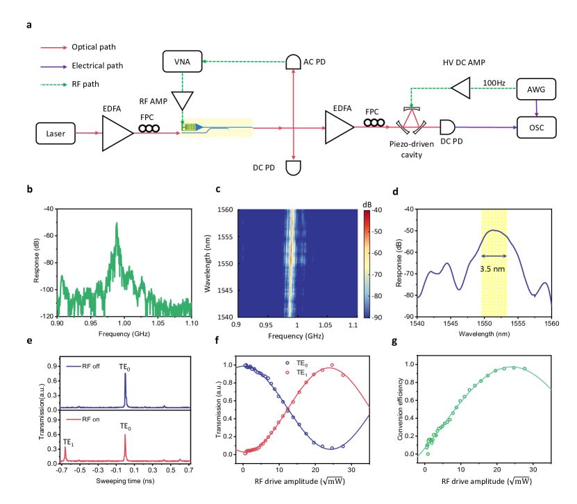
The modulation response is characterized by the measurement setup illustrated in Fig. 3a. CW light generated by a tunable semiconductor laser is amplified by the erbium-doped fiber amplifier (EDFA) and delivered to the device with a lensed fiber. RF signals from the vector network analyzer (VNA) is loaded into IDTs after amplification to excite acoustic fields. The optical transmission is monitored by a slow high-sensitivity photodetector (DC PD). The output optical field is also measured by a fast photodetector (AC PD), whose electric signal is sent back to VNA. The representative RF modulation spectrum is shown in Fig. 3b. The input optical wavelength is set at 1551.7 nm. Strong modulation can be clearly observed. The acoustic modulation 3-dB bandwidth is measured as = 0.57 MHz. With the modulation bandwidth and acoustic propagation loss, we can calculate the acoustic group velocity 4400 m/s, which agrees with the simulated value (see Supplementary Section 1) [14]. We further measure the RF modulation response at different optical wavelengths (Fig. 3c). The acoustic frequency with maximum modulation efficiency shifts with the optical wavelength, showing the change of the phase-matching condition due to dispersion. Figure 3d shows the peak modulation response at different optical wavelengths with the fixed acoustic frequency = 0.998 GHz. The optical bandwidth of the modulation process is measured as 3.5 nm, which agrees the theoretical value nm with the group refractive index difference between TE0 and TE1 modes [15].
To measure the optical conversion efficiency, we use a free-space cavity with 1-MHz linewidth as the optical filter (Fig. 3a). A piezo-transducer is attached to the free-space cavity mirror to modify the resonant wavelengths. The driving voltage of the piezo-transducer is continuously swept. Therefore, we can separate optical powers from the residual input and converted output optical fields in the time domain (Fig. 3e). Without acoustic fields, we only observe the TE0 input optical field. With acoustic fields, the amplitude of the TE0 input optical field decreases. More importantly, we can observe the emergence of the converted TE1 output optical field. The converted TE1 output optical field only shows up on one side of the residual TE0 input optical field, proving the single-sideband nature of acousto-optic modulation. By increasing the RF drive amplitude, we can observe the sinusoidal oscillation of the optical power between TE0 and TE1 modes (Fig. 3f). With driving power mW, the TE0 power is close to zero with the TE1 mode reaching the maximum amplitude. Therefore, the on-chip conversion efficiency () close to unity can be achieved at driving power mW (Fig. 3g). This further allows us to estimate the acousto-optic coupling coefficient (Supplementary Section 3) [13]
| (1) |
which is more than two orders of magnitude higher than acousto-optic devices without simultaneous sub-wavelength acoustic and optical confinement (Table 1).
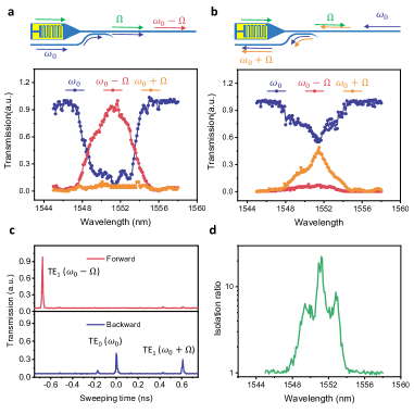
Due to difficulties in integrating high-quality magneto-optical materials, it is challenging to build on-chip optical isolators and circulators. With the direction-dependent phase-matching condition, acousto-optic modulation provides the non-magnetic method to realize on-chip optical isolation [23, 15, 13]. We verify the non-reciprocal behavior of our acousto-optic device by measuring the optical transmission in both forward and backward directions (Fig. 4a and b). The RF driving signal has fixed frequency GHz and power mW. In the forward direction, phase-matching condition is satisfied for the Stokes process, where the input TE0 mode at frequency is converted into the output TE1 mode at frequency (Fig. 4a) [13]. No anti-Stokes signal at frequency is observed. In the backward direction, no mode conversion should happen ideally and all optical power should remain in the TE0 mode at frequency . However, with the finite interaction length, we observe the anti-Stokes process in the backward direction (Fig. 4b). The anti-Stokes process in the backward direction has much lower efficiency due to phase mismatch. Therefore, the input TE0 mode at frequency is only partially converted into the output TE1 mode at frequency even at the maximum modulation optical wavelength nm (Fig. 4c). If we compare the TE0 power in forward and backward directions, we can clearly see that isolation ratio above 10 dB has been achieved (Fig. 4d).
3 Discussion
To benchmark the performance of our device, a summary of recent works on integrated acousto-optic modulators is presented in Table 1. The GaN-on-sapphire platform in this work is the only one that is capable of confining both optical and acoustic fields in sub-wavelength scales without using suspended structures. Therefore, the interaction length has been significantly improved while maintaining the high acousto-optic coupling coefficient. In addition, the GaN-on-sapphire platform also has excellent power-handling capability. No performance degradation is observed under high driving powers (Supplementary Section 4). Moreover, the GaN-on-sapphire platform shows remarkably lower acoustic propagation loss. The excellent performance in all critical merits leads to the demonstration of the near-unity optical conversion efficiency. The robustness of unsuspended structures also allows the incorporation of integrated acousto-optic modulators into large-scale photonic-phononic circuits with complex functionalities. The elimination of supporting tethers and membranes to anchor suspended structures further enables the flexible design of circuit patterns.
The acoustic driving efficiency can be further improved. Propagation loss below 0.05 dB/mm has been demonstrated with GaN-on-sapphire acoustic waveguides [19]. Therefore, the acousto-optic interaction length can be extended by more than 10 times. This will lead to the reduction of the driving power by more than two orders of magnitude, below 10 mW with the current IDT design. The IDT efficiency can be further improved using uni-directional IDT designs with more periods and better electrical impedance matching [24, 25]. The heterogeneous structure of aluminum nitride (AlN) and GaN, which is widely used for power electronics [26], can further increase the driving efficiency by leveraging the larger piezoelectric coefficient in AlN [27]. As a result, we expect the driving power to achieve complete optical conversion can be decreased to the micro-watt level.
| Work | Year | Platform | Suspended | Optical | Acoustic | |||||
|---|---|---|---|---|---|---|---|---|---|---|
| (GHz) | (dB/mm) | (mm) | (mm-1W-1/2) | () | confined | confined | ||||
| Liu [14] | 2019 | AlN | 16.4 | — | 0.5 | 0.041 | 2.5e-4 | Y | Y | Y |
| Kittlaus [15] | 2020 | Si/AlN | 3.11 | — | 0.96 | 4.5 | 13.5 | N | Y | N |
| Christopher [12] | 2020 | LiNbO3 | 0.67 | — | 0.6 | 1.66 | 0.9 | N | Y | N |
| Shao [9] | 2020 | LiNbO3 | 2.89 | — | 0.1 | 0.004 | 3.5 | N | N | N |
| Ahmed [28] | 2021 | LiNbO3 | 1.16 | 4 | 0.45 | 0.417 | 1 | Y | Y | N |
| Christopher [13] | 2021 | LiNbO3 | 0.44 | 11.7 | 0.25 | 377 | 18 | Y | Y | Y |
| Wan [29] | 2022 | LiNbO3 | 0.84 | — | 0.12 | 0.035 | 3.2e-3 | N | Y | N |
| This work | 2023 | GaN | 0.99 | 0.85 | 3 | 255 | 100 | N | Y | Y |
4 Conclusion
In conclusion, we have developed the GaN-on-sapphire platform for acousto-optic devices. We achieve high acousto-optic coupling strength, long interaction length, low-loss acoustic propagation, and large power handling capability at the same time. This leads to the first demonstration of near-unity conversion efficiency with integrated acousto-optic modulators. This work will enable the exploration of hybrid photonic-phoninc circuits at large scale for advanced signal processing, with important applications in microwave photonics and quantum transduction.
Funding This material is based upon work supported by the Office of the Under Secretary of Defense for Research and Engineering under DEPSCoR program award number FA9550-21-1-0225 managed by Army Research Office, and NSF Grant No. ITE-2134830.
Disclosures The Authors declare no competing financial or non-financial interests
Data availability The data that support the findings of this study are available from the corresponding author upon reasonable request
Supplemental document See Supplement 1 for supporting content.
References
- [1] T. J. Kippenberg, A. L. Gaeta, M. Lipson, and M. L. Gorodetsky, “Dissipative kerr solitons in optical microresonators,” \JournalTitleScience 361, eaan8083 (2018).
- [2] D. Marpaung, J. Yao, and J. Capmany, “Integrated microwave photonics,” \JournalTitleNature photonics 13, 80–90 (2019).
- [3] W. Bogaerts, D. Pérez, J. Capmany, D. A. Miller, J. Poon, D. Englund, F. Morichetti, and A. Melloni, “Programmable photonic circuits,” \JournalTitleNature 586, 207–216 (2020).
- [4] A. W. Elshaari, W. Pernice, K. Srinivasan, O. Benson, and V. Zwiller, “Hybrid integrated quantum photonic circuits,” \JournalTitleNature Photonics 14, 285–298 (2020).
- [5] A. H. Safavi-Naeini, D. Van Thourhout, R. Baets, and R. Van Laer, “Controlling phonons and photons at the wavelength scale: integrated photonics meets integrated phononics,” \JournalTitleOptica 6, 213–232 (2019).
- [6] J. Bochmann, A. Vainsencher, D. D. Awschalom, and A. N. Cleland, “Nanomechanical coupling between microwave and optical photons,” \JournalTitleNature Physics 9, 712–716 (2013).
- [7] L. Fan, C.-L. Zou, M. Poot, R. Cheng, X. Guo, X. Han, and H. X. Tang, “Integrated optomechanical single-photon frequency shifter,” \JournalTitleNature Photonics 10, 766–770 (2016).
- [8] K. J. Satzinger, Y. Zhong, H.-S. Chang, G. A. Peairs, A. Bienfait, M.-H. Chou, A. Cleland, C. R. Conner, É. Dumur, J. Grebel et al., “Quantum control of surface acoustic-wave phonons,” \JournalTitleNature 563, 661–665 (2018).
- [9] L. Shao, N. Sinclair, J. Leatham, Y. Hu, M. Yu, T. Turpin, D. Crowe, and M. Lončar, “Integrated microwave acousto-optic frequency shifter on thin-film lithium niobate,” \JournalTitleOptics Express 28, 23728–23738 (2020).
- [10] L. Fan, C.-L. Zou, N. Zhu, and H. X. Tang, “Spectrotemporal shaping of itinerant photons via distributed nanomechanics,” \JournalTitleNature Photonics 13, 323–327 (2019).
- [11] H. Zhao, B. Li, H. Li, and M. Li, “Enabling scalable optical computing in synthetic frequency dimension using integrated cavity acousto-optics,” \JournalTitleNature Communications 13, 5426 (2022).
- [12] C. J. Sarabalis, T. P. McKenna, R. N. Patel, R. Van Laer, and A. H. Safavi-Naeini, “Acousto-optic modulation in lithium niobate on sapphire,” \JournalTitleApl Photonics 5, 086104 (2020).
- [13] C. J. Sarabalis, R. Van Laer, R. N. Patel, Y. D. Dahmani, W. Jiang, F. M. Mayor, and A. H. Safavi-Naeini, “Acousto-optic modulation of a wavelength-scale waveguide,” \JournalTitleOptica 8, 477–483 (2021).
- [14] Q. Liu, H. Li, and M. Li, “Electromechanical brillouin scattering in integrated optomechanical waveguides,” \JournalTitleOptica 6, 778–785 (2019).
- [15] E. A. Kittlaus, W. M. Jones, P. T. Rakich, N. T. Otterstrom, R. E. Muller, and M. Rais-Zadeh, “Electrically driven acousto-optics and broadband non-reciprocity in silicon photonics,” \JournalTitleNature Photonics 15, 43–52 (2021).
- [16] S. A. Tadesse and M. Li, “Sub-optical wavelength acoustic wave modulation of integrated photonic resonators at microwave frequencies,” \JournalTitleNature communications 5, 5402 (2014).
- [17] M. de Lima Jr, M. Beck, R. Hey, and P. Santos, “Compact mach-zehnder acousto-optic modulator,” \JournalTitleApplied physics letters 89, 121104 (2006).
- [18] P. Renosi, J. Sapriel, and B. Djafari-Rouhani, “Resonant acousto-optic effects in inp and gaas and related devices,” in 1993 (5th) International Conference on Indium Phosphide and Related Materials, (IEEE, 1993), pp. 592–595.
- [19] W. Fu, Z. Shen, Y. Xu, C.-L. Zou, R. Cheng, X. Han, and H. X. Tang, “Phononic integrated circuitry and spin–orbit interaction of phonons,” \JournalTitleNature communications 10, 2743 (2019).
- [20] Y. Zheng, C. Sun, B. Xiong, L. Wang, Z. Hao, J. Wang, Y. Han, H. Li, J. Yu, and Y. Luo, “Integrated gallium nitride nonlinear photonics,” \JournalTitleLaser & Photonics Reviews 16, 2100071 (2022).
- [21] G. S. Wiederhecker, P. Dainese, and T. P. Mayer Alegre, “Brillouin optomechanics in nanophotonic structures,” \JournalTitleAPL photonics 4, 071101 (2019).
- [22] X.-B. Xu, J.-Q. Wang, Y.-H. Yang, W. Wang, Y.-L. Zhang, B.-Z. Wang, C.-H. Dong, L. Sun, G.-C. Guo, and C.-L. Zou, “High-frequency traveling-wave phononic cavity with sub-micron wavelength,” \JournalTitleApplied Physics Letters 120, 163503 (2022).
- [23] E. A. Kittlaus, N. T. Otterstrom, P. Kharel, S. Gertler, and P. T. Rakich, “Non-reciprocal interband brillouin modulation,” \JournalTitleNature Photonics 12, 613–619 (2018).
- [24] K. Yamanouchi and Y. Satoh, “Ultra low-insertion-loss surface acoustic wave filters using unidirectional interdigital transducers with grating saw substrates,” \JournalTitleJapanese journal of applied physics 44, 4532 (2005).
- [25] V. T. Rathod, “A review of electric impedance matching techniques for piezoelectric sensors, actuators and transducers,” \JournalTitleElectronics 8, 169 (2019).
- [26] K. H. Hamza and D. Nirmal, “A review of gan hemt broadband power amplifiers,” \JournalTitleAEU-International Journal of Electronics and Communications 116, 153040 (2020).
- [27] M. Rais-Zadeh, V. J. Gokhale, A. Ansari, M. Faucher, D. Théron, Y. Cordier, and L. Buchaillot, “Gallium nitride as an electromechanical material,” \JournalTitleJournal of Microelectromechanical Systems 23, 1252–1271 (2014).
- [28] A. E. Hassanien, S. Link, Y. Yang, E. Chow, L. L. Goddard, and S. Gong, “Efficient and wideband acousto-optic modulation on thin-film lithium niobate for microwave-to-photonic conversion,” \JournalTitlePhotonics Research 9, 1182–1190 (2021).
- [29] L. Wan, Z. Yang, W. Zhou, M. Wen, T. Feng, S. Zeng, D. Liu, H. Li, J. Pan, N. Zhu et al., “Highly efficient acousto-optic modulation using nonsuspended thin-film lithium niobate-chalcogenide hybrid waveguides,” \JournalTitleLight: Science & Applications 11, 145 (2022).