Origin of -shifted three-dimensional charge density waves in kagome metal AV3Sb5
Abstract
Understanding the nature of charge density wave (CDW) and superconductivity in kagome metal AV3Sb5 (A=Cs,Rb,K) is a recent subject of intensive study. Due to the presence of van Hove singularities, electron-electron interaction has been suggested to play an important role in the formation of such broken symmetry states. Recent experiments show that the CDW order is three-dimensional and it is staggered across different kagome layers. However, the experimental interpretation for the precise structure of CDW varies in terms of whether it is the star of David (SD), inverse star of David (ISD) or the alternation of the two among neighboring layers. In this work, we show that the origin of these distinct CDW orders can be understood in a unified picture by considering intra- and inter-layer electron-electron interactions as well as the coupling between electrons and lattice distortions. Utilizing an effective 9-band model with V orbitals and out-of-plane Sb orbitals, it is demonstrated that the repulsive electron-electron interaction favors charge bond order which induces either SD or ISD upon including lattice distortions. As the inter-layer interaction is introduced, -shifted CDW develops with the staggered ordering along the -axis. We also find that the phase with alternating SD and ISD can be stabilized as the ground state under strong inter-layer interaction.
I Introduction
Kagome materials provide a natural platform to study the interplay between many intriguing ingredients such as van-Hove singularities (vHS), flat bands, topology, Dirac cones, and geometric frustration. The family of vanadium-based kagome metal AV3Sb5 (A=Cs,Rb,K) has drawn great attention due to the recent discovery of various exotic phases in these materials [1, 2, 3, 4, 5, 6, 7, 8, 9, 10, 11, 12]. Superconductivity has been observed with [13, 14, 15, 16], which coexists with charge density wave (CDW) with transition temperature [17, 18, 19, 20, 21, 22]. The CDW and SC phases observed in these materials are quite unconventional. Scanning tunnelling microscope (STM) experiments have shown that the CDW order induces lattice distortion in the vanadium kagome layers with enlarged periodicity [23], which is suggestive of the important role played by the vHS proximity to the Fermi level at momenta . Rotational symmetry breaking is found in the CDW phase [24, 25]. Time-reversal symmetry breaking (TRSB) is observed in the CDW phase via muon spin relaxation (SR) and STM experiments [19, 23, 26], and a giant anomalous Hall effect [27] is reported in the absence of magnetism [28]. However, Kerr effect measurements give contradicting results on TRSB [29, 30, 31, 32]. Magnetoresistance measurements in ring structure sample in the superconductivity phase show oscillations corresponding to charge 4 and 6 flux quantization [33], indicating the possibility for novel superconductivity.
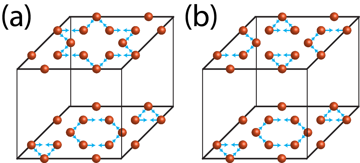
The origin of superconductivity and the detailed structure of CDW still remain elusive. The CDW lattice distortion within the kagome planes compatible with periodicity is the star of David (SD) or inverse star of David (ISD), and the ISD is also called tri-hexagonal phase (TrH). These in-plane orders can also be stacked along the -axis to give three-dimensional CDW order [34]. For example, in addition to the phase with uniform repetition of SD or ISD among different layers, there can be phases with alternating SD and ISD orders in neighboring layers as shown in Fig.1(a), or phases solely made of ISD(SD) but the CDW pattern is -shifted between neighboring layers as in Fig.1(b), which is known as -shifted ISD(SD) phase. Various experimental and theoretical techniques are applied to determine the structure of CDW [35, 11, 36, 37, 38, 39, 40, 41, 42, 43, 44, 45, 46, 47, 48, 49, 50, 51, 52, 53, 54, 55, 56, 40] and the results are diverse. The nuclear magnetic resonance (NMR) and nuclear quadrupolar resonance (NQR) experiments in Refs.57 show that the CDW order is the -shifted (staggered) ISD, whereas Ref.44 also performs NMR and NQR experiments but concludes that the CDW order is SD, and the combination of angle-resolved photoemission spectroscopy (ARPES) and density functional theory (DFT) in Ref.42 suggests the CDW order is the alternating SD and ISD order between neighboring layers. Therefore, a comprehensive understanding of the CDW order is highly desirable.
Given the close relationship between superconductivity and CDW in this family of kagome materials, identifying the nature of CDW can shed light on the study of superconductivity. For example, the symmetry and dimensionality of the CDW order parameter are crucial for modeling the normal state upon which the superconductivity is developed, and the mechanism that leads to the CDW order can provide valuable insight into the origin of superconductivity. The proximity of the van-Hove singularities at momentum to the Fermi level suggests that investigating the role played by electron interaction is crucial for understanding the nature of CDW and superconductivity.
In this work, we show that the distinct CDW orders observed in experiments can be understood in a unified picture by considering electron interaction and the coupling between electron and lattice distortion. We construct a tight-binding model with both the orbitals from vanadium sites and orbitals from out-of-plane antimony sites using hopping parameters obtained from realistic DFT computation. Our mean-field computation shows that the intra-layer repulsive interaction stabilizes the electronic charge bond order (CBO) that involves three distinct points in the Brillouin zone. Furthermore, the inter-layer interaction along the -axis favors non-uniform alignment of CBO among neighboring layers because it reduces the repulsion. Through the coupling between electron and lattice distortion, the CBO induces lattice distortion of either ISD or SD within each kagome layer. If inter-layer interaction is weak, it favors the -shifted ISD or -shifted SD order depending on the sign of electron-lattice coupling. If inter-layer interaction is strong, the phase with alternating ISD and SD in neighboring layers can be stabilized as the ground state because it can further lower the repulsive interaction. Therefore, this mechanism is a potential reason to explain the distinct three-dimensional CDW orders with enlarged periodicity observed in experiments.
II Tight-binding model with and orbitals
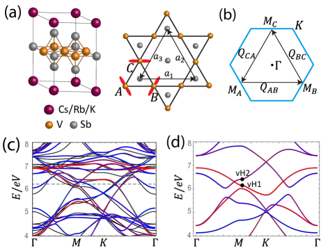
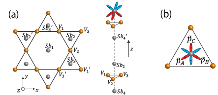
The crystal structure of AV3Sb5 is characterized by the kagome planes of vanadium sites as shown in Fig.2(a), with one in-plane antimony Sb1 and four out-of-plane antimony Sb2 inside each unit cell. The bands near Fermi energy are made of superpositions of orbitals from vanadium sites and orbitals from antimony sites. We construct a tight-binding model by taking into account all these and orbitals, and determine the hopping amplitude among these orbitals by comparing with first-principle DFT bands for CsV3Sb5. This procedure yields a 30-band tight-binding model with five orbitals at each vanadium site and three orbitals at each antimony site. We choose the unit cell to contain three vanadium sites denoted by at an upper triangle as in Fig.2(a) and the antimony sites above and below the vanadium plane. This model includes up to second nearest neighbor in-plane V-V hopping and nearest neighbor V-Sb2, V-Sb1, Sb2-Sb2, Sb1-Sb2 hoppings. The band structure obtained from this model is shown in Fig.2(c), which agrees reasonably well with DFT computation. More details of this model are given in the appendix. The only inter-layer hopping is the hopping between out-of-plane Sb2 atoms that are connecting different unit cells separated vertically along the -axis. If , then different layers are decoupled and the band dispersion does not depend on . In reality there is a small hopping and the bands are weakly dispersing along the z direction.
To study the CDW phase with periodicity, we aim to simplify the model by focusing on the vHS at point of the Brillouin zone which mainly consists of and orbitals from vanadium sites. By choosing a suitable linear combination of and orbitals at each vanadium sites as the red orbitals in Fig.2(a), we find that the orbitals () contribute more than 80% weight of the wave function near the vHS as shown in the appendix. Therefore, among the five orbitals at each vanadium sites we keep only one orbital. We also neglect the three orbitals at the in-plane antimony site Sb1, because these orbitals mainly contribute to the point and have little contribution to the vHS. This reduces the 30-band model to a 15-band model with three orbitals and twelve orbitals at the four out-of-plane Sb2 sites.
We can further simplify this model by noticing that the orbitals at sites below and above the kagome plane can be superimposed to yield orbitals with positive or negative eigenvalues of the in-plane mirror symmetry . The wave function at the vHS must be an eigenstate of . Since the orbitals have negative eigenvalue of , then among the twelve orbitals only the six orbitals with negative eigenvalue can contribute to the wave function at the vHS. Therefore we arrive at a 9-band model with three orbitals and six orbitals coming from linear combinations of out-of-plane orbitals with negative eigenvalues.
The band structure of this 9-band model is shown in Fig.2(d). The color of the bands represent the weight of wave function at vanadium orbitals and antimony orbitals. The red (blue) bands have more weight at () orbitals. The vHS can be seen at the points of the Brillouin zone, which are denoted by vH1 and vH2. The vH point vH1 is dominated by vanadium orbitals, while vH2 is a mixture of and orbitals. The dispersion away from the vH point deviates from the actual DFT band structure due to the fact that the model captures the band structure near the vHS while the features away from the vHS are neglected.
Compared with the commonly used three-band single-orbital model on kagome lattice, this model also includes the orbitals at the out-of-plane Sb2 sites. These orbitals are important in modeling the CDW phenomena [53, 58, 40]. They are essential not only in reproducing the band structure close to DFT as in Fig.2(c), but also in capturing the nature of vHS vH1 and vH2. vH2 is a mixture of and orbitals, which will not exist if the orbitals of Sb2 are not included. For the pristine type of vH point vH1 mostly made of orbitals, the orbitals are still important because the hopping modifies the effective hopping between orbitals to give it a correct sign. When modeling vH1 via the simple three-band model with only one orbital at each vanadium site, the hopping between nearest neighbor sites needs to be negative [49, 56, 55] to make the energy along higher than in the vicinity of vH1, as in Fig.2(d). However, our DFT computation shows the bare hopping between nearest neighbor orbitals is positive, and the hopping between and orbitals are comparable or even larger than the hopping (see the appendix for details). Therefore, the negative effective hopping between orbitals necessary for vH1 must come from the large coupling between and orbitals. This demonstrates the important role of orbitals from Sb2 sites in modeling the van-Hove singularities.
III Order parameter for different charge density waves
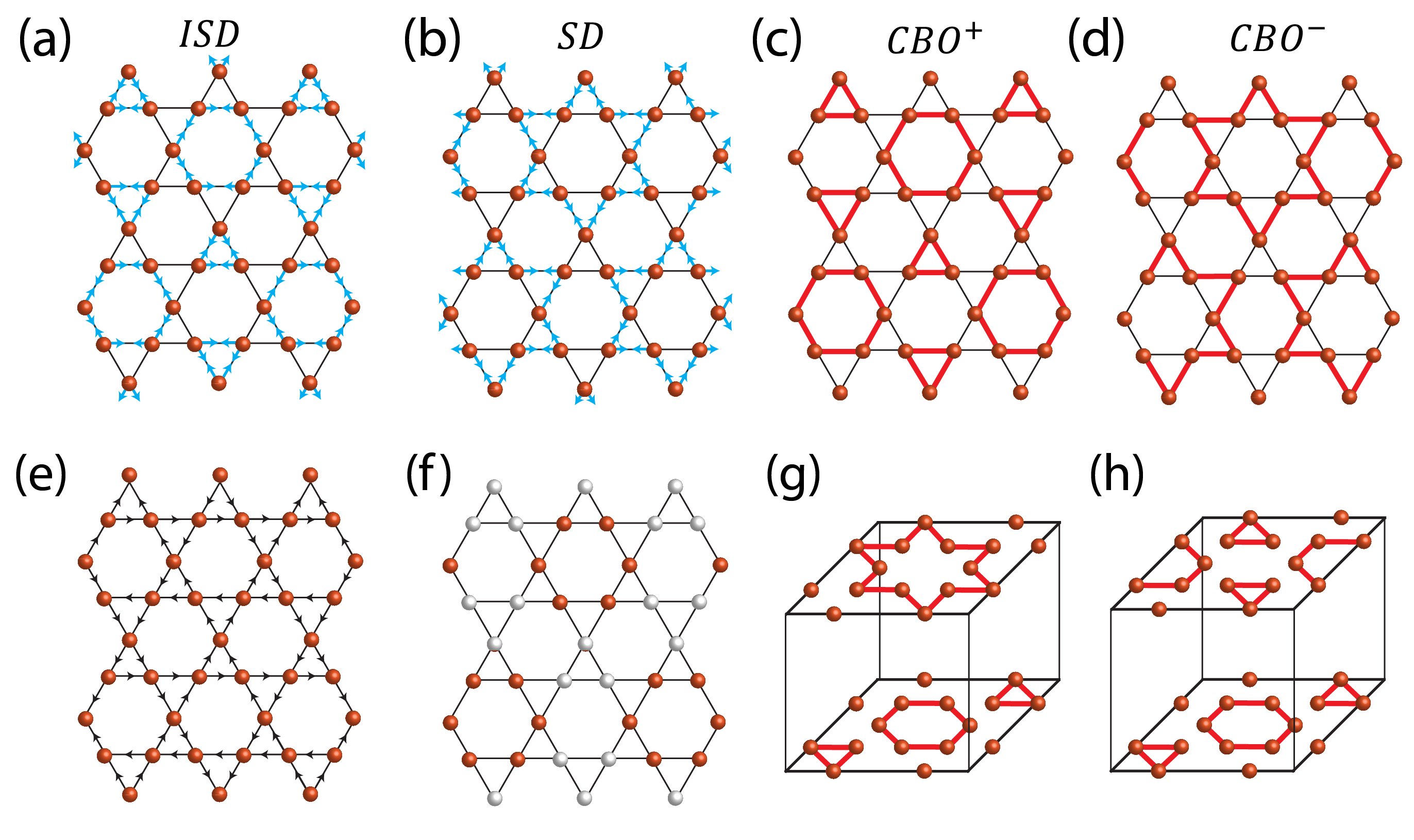
Various of order parameters can lead to the enlarged periodicity within kagome planes. The order parameters can represent lattice distortion with the ordering wave vector at the three inequivalent points in the Brillouin zone. As shown in Fig.3(a,b), the kagome lattice of vanadium atoms can be distorted to form patterns of star of David (SD) or inverse star of David (ISD). The displacement of each site is the vector sum of the two arrows at that site. This distortion breaks the original translational symmetry and enlarges the unit cell. Without loss of generality we choose the unit cell to contain the three sites in the same upper triangle, i.e., the A,B,C sites in Fig.2(a). Label each unit cell by and denote the strength of the arrows parallel to AB, BC, CA directions by respectively, then the ISD and SD phases with periodicity satisfy:
| (1) |
Here can take and and are vectors connecting different points in the Brillouin zone as shown in Fig.2(b). Each cosine factor in Eq.(1) is . represents an ISD phase and represents and SD phase. Note that if the sign of one of the three ’s in an ISD (SD) phase is flipped, the phase will turn into SD (ISD) phase. If two of the three ’s are flipped, the type of the phase remains the same, but it is shifted by one lattice constant compared with the original phase.
In addition to lattice distortion, electron-electron interaction can also lead to a broken translational symmetry with an enlarged unit cell. This includes the charge bond order (CBO), charge density order (CDO) and loop current order (LCO). Denote the electron creation operator of orbital at vanadium site of unit cell by . The order parameter is given by:
| (2) |
Here is the number of unit cell, can be and respectively, where and are shown in Fig.2(a). The CBO and LCO phases are given by the real and imaginary part of . If is real, then the corresponding CBO phases with (CBO+) and (CBO-) represent different modulations of at nearest neighbor bonds, which are shown in Fig.3(c) and (d) respectively. As we will show later, when the coupling between electron and lattice distortion is considered, CBO+ will be stabilized as the ground state, which can induce ISD lattice distortion.
If is imaginary, it represents the LCO with finite current on nearest neighbor bonds. The LCO with is shown in Fig.3(e), where the arrows represent the direction of current on each bond. Contrary to the phases with lattice distortion or CBO, the LCO phase breaks time-reversal symmetry and can lead to the anomalous Hall effect.
There can also be CDO as shown in Fig.3(f) which modifies the electron density at each site. The order parameter is:
| (3) |
Here . Fig.3(f) corresponds to with the origin chosen to be at the shaded upper triangle.
The order parameters in neighboring kagome layers can also be alternated to produce three-dimensional CDW order with periodicity. For example, among the CBO phases, if the signs of are alternating between neighboring layers as shown in Fig.3(g), it leads to a phase with alternating CBO+ and CBO-. This pattern is similar to Fig.1(a) but it represents electronic order rather than lattice distortion. If only and have alternating signs between layers and is fixed, the resulting phase is a -shifted CBO+ phase as shown in Fig.3(h). This pattern is similar to Fig.1(b) but without lattice distortion. If the sign of alternates along z direction between layers, the ordering wave vector no longer connects points, but involves points in the Brillouin zone with . Let , then this new order parameter is defined as:
| (4) |
The phase with -shifted CBO+ in Fig.3(h) is represented by , which is also denoted by indicating it has one component at point and two components at point. The phase in Fig.3(g) is given by , which is denoted by . Similar notations can also describe lattice distortion with alternating signs at different layers, this can be done by replacing and in Eq.(1) by and respectively.
IV Full Hamiltonian: electron interaction and coupling to lattice distortion
Various CDW orders can be induced by electron interaction. We consider systems at the filling of vH1 in Fig.2(d). The wave function at this vHS is dominated by orbitals which are superpositions of and orbitals at vanadium kagome sites as presented above. The Hamiltonian is written as:
| (5) |
The non-interacting part is the 9-band tight-binding model in Sec.II. is the electron interaction between orbitals at kagome sites. Let denote both the unit cell and sublattice such that , is given by:
| (6) |
Here and is the lattice constant along z direction. The term represent nearest neighbor (NN) interaction inside kagome plane, and the term represent interaction between sites at neighboring kagome layers that are on top of each other. is the elastic energy from lattice distortion in the kagome plane:
| (7) |
Here is the spring constant and is the NN bond length without distortion. and are restricted to be nearest neighbors inside the same kagome plane. is the change of distance between sites labeled by and due to lattice distortion, which can be rewritten straightforwardly using in Eq.(1). For example, for the AB bond at an upper triangle in the unit cell labeled by , the change of bond length is given by . is the coupling between electron and lattice distortion. Let the in-plane displacement of each site be which is the vector sum of connected to site , is given by:
| (8) | |||||
The term comes from the change of effective hopping strength due to the change of bond length . If the hopping term is with and , Taylor expansion leads to , which gives . If is positive, then a NN bond with can induce a shrink of bond length, i.e., the CBO+ (CBO-) phase can induce ISD (SD) phase through coupling between electron and lattice distortion. In practice, the sign of may depend on microscopic details. The term comes from the fact that when , the two sites with interaction are separated further, which reduces the interaction and leads to Eq.(8) with . Note that the displacement and the change of bond length can be written in terms of and in Eq.(1). Therefore we will use as the order parameter to represent lattice displacement.
V Mean field analysis of charge density waves
V.1 Two-dimensional order parameters within kagome planes
We use mean field theory to determine which order parameter is favored in the ground state. For simplicity we first study the effective two-dimensional system obtained by turning off the coupling between different kagome layers, which includes terms and the inter-layer hopping between different Sb2 sites in different unit cells. In this limit the band structure becomes two-dimensional and does not depend on .
The repulsive interaction at NN bonds can be decoupled by a Hubbard-Stratonovich (H-S) transformation. Define the Fourier transformation of electronic operator as . For bonds along direction () at an upper-triangle of the kagome lattice, the interaction and its mean-field decoupling are given by:
| (9) |
Here we only keep in accordance with the CDW. We have introduced in the H-S transformation. Since we have chosen the unit cell to contain three sites at upper triangles, for the bonds at down triangles the transformation of has an additional -dependent phase. The corresponding interaction and its mean-field decoupling are:
| (10) |
where . The mean field Hamiltonian is obtained by replacing the term in Eq.(5) by Eq.(9) and (10), and is summed over AB,BC and CA. The simultaneous presence of gives rise to the periodicity and shrinks the Brillouin zone to one-quarter of its original size. The free energy can be computed from the eigenvalues of . When lattice distortion described by is also considered, is a function of and with . Minimization of by changing these variables gives the mean field solution for these order parameters.
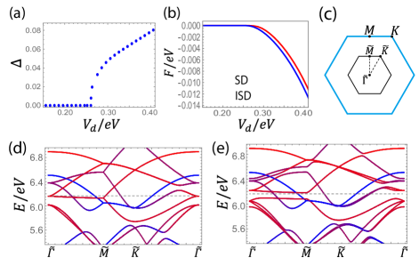
We find a finite mean field solution corresponding to the global minimum of free energy when increases. The solution shows both and are real numbers, and they always have opposite sign . Therefore the solution can be characterized by their difference . Note that the here is the same as the order parameter in Eq.(2). The mean field solution also preserves the threefold rotation symmetry, with and . When the electron-lattice coupling is positive, the solution has and , which represents coexisting phases of electronic charge bond order CBO+ and lattice distortion with ISD pattern. If the sign of is flipped , the solution shows that remains positive but becomes negative, representing SD type of lattice distortion. Without loss of generality, from now on we focus on the case with . as a function of is shown in Fig.4(a) with the parameter choice where is the temperature. The phase with CBO- and SD lattice distortion () is a local minimum of free energy, but not the global minimum. The free energy for phases with ISD () and SD () order are shown in Fig.4(b), which shows ISD phase has lower free energy. The free energy is not an even function of order parameters as seen by the energy difference between SD and ISD phases, hence the phase transition that leads to a finite is different from a usual second-order transition.
The order parameters in the mean field solutions are real numbers. We find that the solution with imaginary corresponding to the LCO can be local minimum of free energy when interaction is large, but it has higher energy than the real CBO order. Hence the LCO is not the ground state in our computation. This is consistent with Ref. 56 which shows that complex charge bond order corresponding to loop current phases only occurs when there is large second-nearest neighbor interaction.
The band structure in the reduced Brillouin zone (Fig.4(c)) before and after the development of the ISD phase is shown in Fig.4(d,e). When , the band structure is in Fig.4(d). The dashed line represents vH1 and the red (blue) bands are dominated by () orbitals. At finite interaction , ISD order is developed with and the band structure is in Fig.4(e). The ISD order opens a gap near the vHS which is dominated by orbitals at vanadium sites, but due to the presence of other orbitals at antimony sites the system remains a metal after the charge order is developed.
V.2 Three-dimensional structure of order parameters
Now we turn on finite interaction along z direction and recover the realistic inter-layer hopping to study the three-dimensional order parameters. The interaction can be rewritten as , therefore it favors a phase with which will lower the repulsion, i.e., a phase with and . To be consistent with the periodicity in the kagome plane, a natural choice of the order parameter is the three-dimensional generalization of Eq.(3):
| (11) | |||||
where and . is manifestly a real number as seen from its definition. These order parameters represent charge density wave patterns of Fig.3(f) which alternate between neighboring layers. The term is written as:
Keeping only , and its mean-field decoupling are:
| (12) |
For the term in Eq.(8), we approximate the electron density operator by the average density which is taken to be a constant. The mean field Hamiltonian also contains the three-dimensional generalization of Eq.(9) and (10) obtained by replacing by and the lattice distortion which involves . The free energy is a function of 15 variables . By minimizing the free energy, we can find several types of local minima corresponding to phases that satisfy self-consistency conditions. We list some of these phases as follows:
| (13) |
Here , , , and are real numbers obtained by minimizing the free energy with and being positive, and . () represents ISD (SD) lattice distortion and charge bond order that is uniform along the z direction. represents alternating ISD and SD patterns between neighboring layers as in Fig.1(a) and Fig.3(g). represents ISD phase which is -shifted between neighboring layers as in Fig.1(b) and Fig.3(h). The small appearing in is due to the broken threefold rotational symmetry. The free energy of these phases as a function of is shown in Fig.5(a). Here we set . It shows that order parameters develop as increases, and the -shifted ISD phase labeled by has the lowest free energy. A typical value of in Eq.(13) at is given by . The parameter in as a function of is shown in Fig.5(b).
The ordering of these phases can be understood by examining the dependence of on at a fixed , as shown in Fig.5(c). When , different layers are almost decoupled, then according to Sec.V.1 the layers with ISD order have lower free energy than those with SD order. The free energy of and are almost degenerate because they both represent ISD phases in all layers. There is a small splitting of free energy between them due to the small inter-layer hopping . The phase has higher free energy because it represents SD order, and the free energy of is in the middle between and because it represents alternating ISD and SD orders. As and increase, it favors a phase that is non-uniform along the z direction so that the effect of repulsive interaction can be reduced. Therefore, with small and , the free energy of decreases and it becomes the ground state.
If and become large, is energetically more favorable than and becomes the ground state. This is because the charge order in neighboring layers of are fully anti-aligned, which further reduces the repulsive interaction along the z direction. The phase diagram as a function of and is shown in Fig.5(d). Here we choose . It shows the order parameters will develop as increases, and the ground state is the -shifted ISD phase labeled by when is small. At a large , there is a first-order phase transition to alternating ISD and SD phase labeled by .
VI Discussion
In order to take into account the electronic structure near the Fermi energy, we constructed an effective 9-band tight-binding model with V orbitals and out-of-plane Sb orbitals. We then studied the effect of intra- and inter-layer nearest-neighbor repulsive interactions on the formation of various CDW phases. Our mean field computation has shown that various three-dimensional CDW orders arise via repulsive electron interactions and electron-lattice coupling. When the intra-layer interaction is strong enough, it stabilizes the CBO+ phase as the ground state, which further induces ISD or SD lattice distortion depending on the sign of electron-lattice coupling. With weak inter-layer interaction , the -shifted (along the -axis) CDW represented by is preferred because it has lower repulsion from in comparison with the uniform charge order along the -axis. This staggered CDW phase breaks the sixfold rotation symmetry down to twofold rotation, which is consistent with the observation in Refs. 24, 25. When becomes strong, the phase with alternating SD and ISD will be the ground state because it can further reduce the repulsion from . The emergence of these different CDW phases depends on microscopic parameters in the system and is sensitive to perturbations, which may explain the fact that these different CDW phases have all been reported in various experiments [40, 57, 44, 42]. The LCO with time-reversal symmetry breaking has not been found in our computation as the CBO order parameter is real. This is consistent with Ref.56 which shows that the LCO does not occur unless there is large second-nearest-neighbor electron interaction comparable to nearest-neighbor interaction. The mechanism for time-reversal symmetry breaking is an important question that remains to be explored. Furthermore, the impact of the -shifted CBO on superconductivity is another intriguing subject for future study.
VII Acknowledgement
This work is supported by the Natural Sciences and Engineering Research Council of Canada (NSERC) and the Center for Quantum Materials at the University of Toronto. H.Y.K acknowledges the support by the Canadian Institute for Advanced Research (CIFAR) and the Canada Research Chairs Program. Y.B.K. is supported by the Simons Fellowship from the Simons Foundation and the Guggenheim Fellowship from the John Simon Guggenheim Memorial Foundation. Computations were performed on the Niagara supercomputer at the SciNet HPC Consortium. SciNet is funded by: the Canada Foundation for Innovation under the auspices of Compute Canada; the Government of Ontario; Ontario Research Fund - Research Excellence; and the University of Toronto.
Appendix A Parameters in the tight-binding model
Here we provide details of the tight-binding model introduced in Sec.II. It involves five orbitals at the three vanadium sites and and three orbitals at the five antimony sites, hence there are 30 bands in total. For definiteness, we focus on CsV3Sb5 and obtain the hopping amplitudes and onsite potentials from DFT computation. The labeling of sites and the directions of coordinate axes are shown in Fig.S1. We choose the basis and for and orbitals respectively. We denote the onsite potential at site by matrix , which represents a term in the Hamiltonian where represent orbitals at site . The hopping amplitude between sites and is denoted by matrix , representing a term in the Hamiltonian. Due to the crystalline symmetry , the three vanadium sites are related by rotation and their onsite potentials are not independent. The onsite potential at site is given by:
| (S1) |
Here the basis is and the unit is . The zeros in the matrix are required by symmetry. The onsite potential at and can be obtained by symmetry.
For antimony sites, the four out-of-plane sites are related by symmetry. Choosing the orbital basis , the onsite potentials at and are:
| (S2) |
| (S3) |
We include the NN and NNN hopping amplitudes between vanadium sites, which are given by:
| (S4) |
| (S5) |
From we can obtain the hopping between nearest neighbor orbitals. Under the basis , the sixfold rotation operator is given by
| (S6) |
The orbital can be transformed into orbital by a rotation at site , or by a rotation at site . Therefore, the hopping between orbitals is the (1,1) element of matrix . Let the creation operator for orbital at site be . A direct computation shows , representing a term in the Hamiltonian with being positive.
The hopping between vanadium and antimony sites are given as follows. It shows that the hopping between V and Sb sites are comparable or even larger than the hopping between vanadium sites.
| (S7) |
| (S8) |
| (S9) |
The hopping between antimony sites are:
| (S10) |
| (S11) |
| (S12) |
| (S13) |
| (S14) |
All these matrices describe distinct hopping processes that are unrelated by symmetry, and the full model is generated by acting elements of to each hopping process. Among these hopping processes, only connects different unit cells separated along the -axis. This is the term mentioned in the main text. If is set to zero, the band dispersion will be uniform along .
We can simplify this tight-binding model by focusing on the van-Hove singularities at point which mainly consists of and orbitals at vanadium sites. By choosing a suitable linear combination of and orbitals at each vanadium sites as indicated by the red orbitals in Fig.2(a), the orbitals () contribute more than 80% weight of the wave function at the vH points. The orbitals are given by:
| (S15) |
We keep only one orbital out of the five orbitals at each vanadium sites. We also neglect the three orbitals at the in-plane antimony site, because these orbitals mainly contribute to the point and have little contribution to the vH point. This reduces the 30-band model to a 15-band model with three orbitals and twelve orbitals at the four out-of-plane Sb sites.
We can further simplify this model by finding a more symmetric basis for the orbitals. For each Sb site, instead of using the global directions for the orbitals, we can use the rotated basis in which the projections of the three orthogonal orbitals in the kagome plane are symmetrically aligned with the neighboring vanadium sites, as in Fig.S1(b). Denote these orbitals by whit , which are given by:
| (S16) |
The orbitals at the other out-of-plane Sb sites are generated by transforming Eq.(S16) by reflection symmetry across the kagome plane and twofold rotation around vanadium sites. Noticing that the orbitals at sites below and above the kagome plane can be superimposed to yield orbitals with positive or negative eigenvalues of the in-plane mirror symmetry . The wave function at the vH point must be an eigenstate of . Since the orbitals have negative eigenvalues of , then among the twelve orbitals only the six orbitals with negative eigenvalue can contribute to the wave function at the vH point. Denote these six orbitals by with and representing the two sublattices of Sb sites above the kagome plane, e.g., is the superposition of at Sb3 and its mirror image with eigenvalue , and is the superposition of at Sb2 and Sb4 with eigenvalue . The similar superposition with eigenvalue is denoted as . Combining the three orbitals and the six orbitals, we obtain the basis for the 9-band model mentioned in the main text.
To obtain the matrix for this 9-band model, we first need to perform a unitary transformation to the 30-band model. The original 30-band model can be obtained from the DFT parameters in Eqs.(S1)-(S14). The ordering of the orbitals in are chosen as according to Fig.S1(a) with Sb5 being the mirror image of Sb3 below the kagome plane. Here represents the five orbitals at site and represents the three orbitals at site Sbi. The directions in these orbitals refer to the global coordinate directions in Fig.S1(a). We apply a unitary transformation to rotate the basis such that it involves the local and orbitals:
| (S17) |
The matrices and are given as follows. Define matrices:
| (S18) |
Here comes from Eq.(S16) and gives the linear superposition between mirror-related sites above and blow the kagome plane. The threefold rotation matrix is with defined in Eq.(S6). let be the identity matrix. Denote as the diagonal block of a matrix made of the -th to -th rows and columns. Then is defined by , , , , . Here is the direct product. is defined by replacing the 21-th and 24-th diagonal elements of by , i.e., and the other elements of is the same as . The matrix takes into account the different orientations of orbitals at sites above and below the kagome plane because flips sign under mirror symmetry , and the matrix implements the rotation to the new local basis involving and orbitals.
The orbitals in the 9-band model are , which correspond respectively to the 1,6,11,19,20,21,25,26,27-th orbitals of the rotated Hamiltonian obtained via Eq.(S17). By performing another unitary transformation such that these nine orbitals become the first nine orbitals, we arrive at a matrix in which the first nine orbitals are given by . Then the matrix of the 9-band model discussed in the main text is obtained by the first block of .
The dispersion of this 9-band model is in Fig.2(d). It captures the van-Hove singularities vH1 and vH2. Using the basis , the components of the squared wave function at vH1 at momentum is with . Therefore vH1 is dominated by orbitals. The squared wave function at vH2 at momentum is with . Therefore vH2 is a mixture of and orbitals. The simple form of wave function is due to our choice of symmetric basis, which is helpful for modeling the van-Hove singularities.
References
- Jiang et al. [2022a] K. Jiang, T. Wu, J.-X. Yin, Z. Wang, M. Z. Hasan, S. D. Wilson, X. Chen, and J. Hu, Kagome superconductors AV3Sb5 (A=K, Rb, Cs), National Science Review 10.1093/nsr/nwac199 (2022a), nwac199, https://academic.oup.com/nsr/advance-article-pdf/doi/10.1093/nsr/nwac199/46104656/nwac199.pdf .
- Neupert et al. [2022] T. Neupert, M. M. Denner, J.-X. Yin, R. Thomale, and M. Z. Hasan, Charge order and superconductivity in kagome materials, Nature Physics 18, 137 (2022).
- Wang et al. [2020] Y. Wang, S. Yang, P. K. Sivakumar, B. R. Ortiz, S. M. L. Teicher, H. Wu, A. K. Srivastava, C. Garg, D. Liu, S. S. P. Parkin, E. S. Toberer, T. McQueen, S. D. Wilson, and M. N. Ali, Proximity-induced spin-triplet superconductivity and edge supercurrent in the topological kagome metal, (2020), arXiv:2012.05898 .
- Hu et al. [2022a] Y. Hu, X. Wu, B. R. Ortiz, S. Ju, X. Han, J. Ma, N. C. Plumb, M. Radovic, R. Thomale, S. D. Wilson, A. P. Schnyder, and M. Shi, Rich nature of van hove singularities in kagome superconductor csv3sb5, Nature Communications 13, 2220 (2022a).
- Oey et al. [2022] Y. M. Oey, B. R. Ortiz, F. Kaboudvand, J. Frassineti, E. Garcia, R. Cong, S. Sanna, V. F. Mitrović, R. Seshadri, and S. D. Wilson, Fermi level tuning and double-dome superconductivity in the kagome metal , Phys. Rev. Mater. 6, L041801 (2022).
- Christensen et al. [2022] M. H. Christensen, T. Birol, B. M. Andersen, and R. M. Fernandes, Loop currents in kagome metals: Multipolar and toroidal magnetic orders, Phys. Rev. B 106, 144504 (2022).
- Zhu et al. [2022] C. C. Zhu, X. F. Yang, W. Xia, Q. W. Yin, L. S. Wang, C. C. Zhao, D. Z. Dai, C. P. Tu, B. Q. Song, Z. C. Tao, Z. J. Tu, C. S. Gong, H. C. Lei, Y. F. Guo, and S. Y. Li, Double-dome superconductivity under pressure in the v-based kagome metals ( and k), Phys. Rev. B 105, 094507 (2022).
- Stahl et al. [2022a] Q. Stahl, D. Chen, T. Ritschel, C. Shekhar, E. Sadrollahi, M. C. Rahn, O. Ivashko, M. v. Zimmermann, C. Felser, and J. Geck, Temperature-driven reorganization of electronic order in , Phys. Rev. B 105, 195136 (2022a).
- Wu et al. [2022] S. Wu, B. R. Ortiz, H. Tan, S. D. Wilson, B. Yan, T. Birol, and G. Blumberg, Charge density wave order in the kagome metal , Phys. Rev. B 105, 155106 (2022).
- Kang et al. [2022a] M. Kang, S. Fang, J.-K. Kim, B. R. Ortiz, S. H. Ryu, J. Kim, J. Yoo, G. Sangiovanni, D. Di Sante, B.-G. Park, C. Jozwiak, A. Bostwick, E. Rotenberg, E. Kaxiras, S. D. Wilson, J.-H. Park, and R. Comin, Twofold van hove singularity and origin of charge order in topological kagome superconductor csv3sb5, Nature Physics 18, 301 (2022a).
- Li et al. [2021] H. Li, T. T. Zhang, T. Yilmaz, Y. Y. Pai, C. E. Marvinney, A. Said, Q. W. Yin, C. S. Gong, Z. J. Tu, E. Vescovo, C. S. Nelson, R. G. Moore, S. Murakami, H. C. Lei, H. N. Lee, B. J. Lawrie, and H. Miao, Observation of unconventional charge density wave without acoustic phonon anomaly in kagome superconductors (, cs), Phys. Rev. X 11, 031050 (2021).
- Wu et al. [2021] X. Wu, T. Schwemmer, T. Müller, A. Consiglio, G. Sangiovanni, D. Di Sante, Y. Iqbal, W. Hanke, A. P. Schnyder, M. M. Denner, M. H. Fischer, T. Neupert, and R. Thomale, Nature of unconventional pairing in the kagome superconductors (), Phys. Rev. Lett. 127, 177001 (2021).
- Ortiz et al. [2020a] B. R. Ortiz, S. M. L. Teicher, Y. Hu, J. L. Zuo, P. M. Sarte, E. C. Schueller, A. M. M. Abeykoon, M. J. Krogstad, S. Rosenkranz, R. Osborn, R. Seshadri, L. Balents, J. He, and S. D. Wilson, : A z2 topological kagome metal with a superconducting ground state, Phys. Rev. Lett. 125, 247002 (2020a).
- Ortiz et al. [2021a] B. R. Ortiz, P. M. Sarte, E. M. Kenney, M. J. Graf, S. M. L. Teicher, R. Seshadri, and S. D. Wilson, Superconductivity in the kagome metal , Phys. Rev. Mater. 5, 034801 (2021a).
- Chen et al. [2021a] K. Y. Chen, N. N. Wang, Q. W. Yin, Y. H. Gu, K. Jiang, Z. J. Tu, C. S. Gong, Y. Uwatoko, J. P. Sun, H. C. Lei, J. P. Hu, and J.-G. Cheng, Double superconducting dome and triple enhancement of in the kagome superconductor under high pressure, Phys. Rev. Lett. 126, 247001 (2021a).
- Chen et al. [2021b] H. Chen, H. Yang, B. Hu, Z. Zhao, J. Yuan, Y. Xing, G. Qian, Z. Huang, G. Li, Y. Ye, S. Ma, S. Ni, H. Zhang, Q. Yin, C. Gong, Z. Tu, H. Lei, H. Tan, S. Zhou, C. Shen, X. Dong, B. Yan, Z. Wang, and H.-J. Gao, Roton pair density wave in a strong-coupling kagome superconductor, Nature 599, 222 (2021b).
- Ortiz et al. [2019] B. R. Ortiz, L. C. Gomes, J. R. Morey, M. Winiarski, M. Bordelon, J. S. Mangum, I. W. H. Oswald, J. A. Rodriguez-Rivera, J. R. Neilson, S. D. Wilson, E. Ertekin, T. M. McQueen, and E. S. Toberer, New kagome prototype materials: discovery of , and , Phys. Rev. Mater. 3, 094407 (2019).
- Ortiz et al. [2020b] B. R. Ortiz, S. M. L. Teicher, Y. Hu, J. L. Zuo, P. M. Sarte, E. C. Schueller, A. M. M. Abeykoon, M. J. Krogstad, S. Rosenkranz, R. Osborn, R. Seshadri, L. Balents, J. He, and S. D. Wilson, : A topological kagome metal with a superconducting ground state, Phys. Rev. Lett. 125, 247002 (2020b).
- Shumiya et al. [2021] N. Shumiya, M. S. Hossain, J.-X. Yin, Y.-X. Jiang, B. R. Ortiz, H. Liu, Y. Shi, Q. Yin, H. Lei, S. S. Zhang, G. Chang, Q. Zhang, T. A. Cochran, D. Multer, M. Litskevich, Z.-J. Cheng, X. P. Yang, Z. Guguchia, S. D. Wilson, and M. Z. Hasan, Intrinsic nature of chiral charge order in the kagome superconductor , Phys. Rev. B 104, 035131 (2021).
- Ortiz et al. [2021b] B. R. Ortiz, S. M. L. Teicher, L. Kautzsch, P. M. Sarte, N. Ratcliff, J. Harter, J. P. C. Ruff, R. Seshadri, and S. D. Wilson, Fermi surface mapping and the nature of charge-density-wave order in the kagome superconductor , Phys. Rev. X 11, 041030 (2021b).
- Si et al. [2022] J.-G. Si, W.-J. Lu, Y.-P. Sun, P.-F. Liu, and B.-T. Wang, Charge density wave and pressure-dependent superconductivity in the kagome metal : A first-principles study, Phys. Rev. B 105, 024517 (2022).
- Song et al. [2022] D. Song, L. Zheng, F. Yu, J. Li, L. Nie, M. Shan, D. Zhao, S. Li, B. Kang, Z. Wu, Y. Zhou, K. Sun, K. Liu, X. Luo, Z. Wang, J. Ying, X. Wan, T. Wu, and X. Chen, Orbital ordering and fluctuations in a kagome superconductor csv3sb5, Science China Physics, Mechanics & Astronomy 65, 247462 (2022).
- Jiang et al. [2021] Y.-X. Jiang, J.-X. Yin, M. M. Denner, N. Shumiya, B. R. Ortiz, G. Xu, Z. Guguchia, J. He, M. S. Hossain, X. Liu, J. Ruff, L. Kautzsch, S. S. Zhang, G. Chang, I. Belopolski, Q. Zhang, T. A. Cochran, D. Multer, M. Litskevich, Z.-J. Cheng, X. P. Yang, Z. Wang, R. Thomale, T. Neupert, S. D. Wilson, and M. Z. Hasan, Unconventional chiral charge order in kagome superconductor kv3sb5, Nature Materials 20, 1353 (2021).
- Zhao et al. [2021] H. Zhao, H. Li, B. R. Ortiz, S. M. L. Teicher, T. Park, M. Ye, Z. Wang, L. Balents, S. D. Wilson, and I. Zeljkovic, Cascade of correlated electron states in the kagome superconductor csv3sb5, Nature 599, 216 (2021).
- Li et al. [2022] H. Li, H. Zhao, B. R. Ortiz, T. Park, M. Ye, L. Balents, Z. Wang, S. D. Wilson, and I. Zeljkovic, Rotation symmetry breaking in the normal state of a kagome superconductor kv3sb5, Nature Physics 18, 265 (2022).
- Mielke et al. [2022] C. Mielke, D. Das, J.-X. Yin, H. Liu, R. Gupta, Y.-X. Jiang, M. Medarde, X. Wu, H. C. Lei, J. Chang, P. Dai, Q. Si, H. Miao, R. Thomale, T. Neupert, Y. Shi, R. Khasanov, M. Z. Hasan, H. Luetkens, and Z. Guguchia, Time-reversal symmetry-breaking charge order in a kagome superconductor, Nature 602, 245 (2022).
- Yang et al. [2020] S.-Y. Yang, Y. Wang, B. R. Ortiz, D. Liu, J. Gayles, E. Derunova, R. Gonzalez-Hernandez, L. Šmejkal, Y. Chen, S. S. P. Parkin, S. D. Wilson, E. S. Toberer, T. McQueen, and M. N. Ali, Giant, unconventional anomalous hall effect in the metallic frustrated magnet candidate, kv¡sub¿3¡/sub¿sb¡sub¿5¡/sub¿, Science Advances 6, eabb6003 (2020), https://www.science.org/doi/pdf/10.1126/sciadv.abb6003 .
- Kenney et al. [2021] E. M. Kenney, B. R. Ortiz, C. Wang, S. D. Wilson, and M. J. Graf, Absence of local moments in the kagome metal kv3sb5 as determined by muon spin spectroscopy, Journal of Physics: Condensed Matter 33, 235801 (2021).
- Xu et al. [2022] Y. Xu, Z. Ni, Y. Liu, B. R. Ortiz, Q. Deng, S. D. Wilson, B. Yan, L. Balents, and L. Wu, Three-state nematicity and magneto-optical kerr effect in the charge density waves in kagome superconductors, Nature Physics 18, 1470 (2022).
- Saykin et al. [2022] D. R. Saykin, C. Farhang, E. D. Kountz, D. Chen, B. R. Ortiz, C. Shekhar, C. Felser, S. D. Wilson, R. Thomale, J. Xia, and A. Kapitulnik, High resolution polar kerr effect studies of csv3sb5: Tests for time reversal symmetry breaking below the charge order transition (2022), arXiv:2209.10570 .
- Hu et al. [2022b] Y. Hu, S. Yamane, G. Mattoni, K. Yada, K. Obata, Y. Li, Y. Yao, Z. Wang, J. Wang, C. Farhang, J. Xia, Y. Maeno, and S. Yonezawa, Time-reversal symmetry breaking in charge density wave of csv3sb5 detected by polar kerr effect (2022b), arXiv:2208.08036 .
- Wang et al. [2023] J. Wang, C. Farhang, B. R. Ortiz, S. D. Wilson, and J. Xia, Resolving the discrepancy between moke measurements at 1550-nm wavelength on kagome metal csv3sb5 (2023), arXiv:2301.08853 .
- Ge et al. [2022] J. Ge, P. Wang, Y. Xing, Q. Yin, H. Lei, Z. Wang, and J. Wang, Discovery of charge-4e and charge-6e superconductivity in kagome superconductor csv3sb5 (2022), arXiv:2201.10352 .
- Kang et al. [2022b] M. Kang, S. Fang, J. Yoo, B. R. Ortiz, Y. M. Oey, J. Choi, S. H. Ryu, J. Kim, C. Jozwiak, A. Bostwick, E. Rotenberg, E. Kaxiras, J. G. Checkelsky, S. D. Wilson, J.-H. Park, and R. Comin, Charge order landscape and competition with superconductivity in kagome metals, Nature Materials 10.1038/s41563-022-01375-2 l (2022b).
- Nie et al. [2022] L. Nie, K. Sun, W. Ma, D. Song, L. Zheng, Z. Liang, P. Wu, F. Yu, J. Li, M. Shan, D. Zhao, S. Li, B. Kang, Z. Wu, Y. Zhou, K. Liu, Z. Xiang, J. Ying, Z. Wang, T. Wu, and X. Chen, Charge-density-wave-driven electronic nematicity in a kagome superconductor, Nature 604, 59 (2022).
- Stahl et al. [2022b] Q. Stahl, D. Chen, T. Ritschel, C. Shekhar, E. Sadrollahi, M. C. Rahn, O. Ivashko, M. v. Zimmermann, C. Felser, and J. Geck, Temperature-driven reorganization of electronic order in , Phys. Rev. B 105, 195136 (2022b).
- Tan et al. [2021] H. Tan, Y. Liu, Z. Wang, and B. Yan, Charge density waves and electronic properties of superconducting kagome metals, Phys. Rev. Lett. 127, 046401 (2021).
- Liang et al. [2021] Z. Liang, X. Hou, F. Zhang, W. Ma, P. Wu, Z. Zhang, F. Yu, J.-J. Ying, K. Jiang, L. Shan, Z. Wang, and X.-H. Chen, Three-dimensional charge density wave and surface-dependent vortex-core states in a kagome superconductor , Phys. Rev. X 11, 031026 (2021).
- Jiang et al. [2022b] Z. Jiang, H. Ma, W. Xia, Q. Xiao, Z. Liu, Z. Liu, Y. Yang, J. Ding, Z. Huang, J. Liu, Y. Qiao, J. Liu, Y. Peng, S. Cho, Y. Guo, J. Liu, and D. Shen, Observation of electronic nematicity driven by three-dimensional charge density wave in kagome lattice kv3sb5 (2022b), arXiv:2208.01499 .
- Ritz et al. [2022] E. T. Ritz, R. M. Fernandes, and T. Birol, Impact of sb degrees of freedom on the charge density wave phase diagram of the kagome metal csv3sb5 (2022), arXiv:2212.13319 .
- Ortiz et al. [2021c] B. R. Ortiz, S. M. L. Teicher, L. Kautzsch, P. M. Sarte, N. Ratcliff, J. Harter, J. P. C. Ruff, R. Seshadri, and S. D. Wilson, Fermi surface mapping and the nature of charge-density-wave order in the kagome superconductor , Phys. Rev. X 11, 041030 (2021c).
- Hu et al. [2022c] Y. Hu, X. Wu, B. R. Ortiz, X. Han, N. C. Plumb, S. D. Wilson, A. P. Schnyder, and M. Shi, Coexistence of trihexagonal and star-of-david pattern in the charge density wave of the kagome superconductor , Phys. Rev. B 106, L241106 (2022c).
- Yang et al. [2022] H.-J. Yang, H. S. Kim, M. Y. Jeong, Y. B. Kim, M. J. Han, and S. Lee, Intertwining orbital current order and superconductivity in kagome metal (2022).
- Luo et al. [2022a] J. Luo, Z. Zhao, Y. Z. Zhou, J. Yang, A. F. Fang, H. T. Yang, H. J. Gao, R. Zhou, and G.-q. Zheng, Possible star-of-david pattern charge density wave with additional modulation in the kagome superconductor csv3sb5, npj Quantum Materials 7, 30 (2022a).
- Mu et al. [2022] C. Mu, Q. Yin, Z. Tu, C. Gong, P. Zheng, H. Lei, Z. Li, and J. Luo, Tri-hexagonal charge order in kagome metal csv3sb5 revealed by 121sb nuclear quadrupole resonance, Chinese Physics B 31, 017105 (2022).
- Luo et al. [2022b] H. Luo, Q. Gao, H. Liu, Y. Gu, D. Wu, C. Yi, J. Jia, S. Wu, X. Luo, Y. Xu, L. Zhao, Q. Wang, H. Mao, G. Liu, Z. Zhu, Y. Shi, K. Jiang, J. Hu, Z. Xu, and X. J. Zhou, Electronic nature of charge density wave and electron-phonon coupling in kagome superconductor kv3sb5, Nature Communications 13, 273 (2022b).
- Kato et al. [2022] T. Kato, Y. Li, T. Kawakami, M. Liu, K. Nakayama, Z. Wang, A. Moriya, K. Tanaka, T. Takahashi, Y. Yao, and T. Sato, Three-dimensional energy gap and origin of charge-density wave in kagome superconductor kv3sb5, Communications Materials 3, 30 (2022).
- Cho et al. [2021] S. Cho, H. Ma, W. Xia, Y. Yang, Z. Liu, Z. Huang, Z. Jiang, X. Lu, J. Liu, Z. Liu, J. Li, J. Wang, Y. Liu, J. Jia, Y. Guo, J. Liu, and D. Shen, Emergence of new van hove singularities in the charge density wave state of a topological kagome metal , Phys. Rev. Lett. 127, 236401 (2021).
- Denner et al. [2021] M. M. Denner, R. Thomale, and T. Neupert, Analysis of charge order in the kagome metal (), Phys. Rev. Lett. 127, 217601 (2021).
- Park et al. [2021] T. Park, M. Ye, and L. Balents, Electronic instabilities of kagome metals: Saddle points and landau theory, Phys. Rev. B 104, 035142 (2021).
- Lin and Nandkishore [2021] Y.-P. Lin and R. M. Nandkishore, Complex charge density waves at van hove singularity on hexagonal lattices: Haldane-model phase diagram and potential realization in the kagome metals (=k, rb, cs), Phys. Rev. B 104, 045122 (2021).
- Christensen et al. [2021] M. H. Christensen, T. Birol, B. M. Andersen, and R. M. Fernandes, Theory of the charge density wave in kagome metals, Phys. Rev. B 104, 214513 (2021).
- Jeong et al. [2022] M. Y. Jeong, H.-J. Yang, H. S. Kim, Y. B. Kim, S. Lee, and M. J. Han, Crucial role of out-of-plane sb orbitals in van hove singularity formation and electronic correlations in the superconducting kagome metal , Phys. Rev. B 105, 235145 (2022).
- Tazai et al. [2022] R. Tazai, Y. Yamakawa, S. Onari, and H. Kontani, Mechanism of exotic density-wave and beyond-migdal unconventional superconductivity in kagome metal av¡sub¿3¡/sub¿sb¡sub¿5¡/sub¿ (a = k, rb, cs), Science Advances 8, eabl4108 (2022), https://www.science.org/doi/pdf/10.1126/sciadv.abl4108 .
- Zhou and Wang [2022] S. Zhou and Z. Wang, Chern fermi pocket, topological pair density wave, and charge-4e and charge-6e superconductivity in kagomé superconductors, Nature Communications 13, 7288 (2022).
- Dong et al. [2022] J.-W. Dong, Z. Wang, and S. Zhou, Loop-current charge density wave driven by long-range coulomb repulsion on the kagome lattice (2022), arXiv:2209.10768 .
- Frassineti et al. [2022] J. Frassineti, P. Bonfà, G. Allodi, E. Garcia, R. Cong, B. R. Ortiz, S. D. Wilson, R. De Renzi, V. F. Mitrović, and S. Sanna, Microscopic nature of the charge-density wave in kagome superconductor rbv3sb5 (2022), arXiv:2210.06523 .
- Tsirlin et al. [2022] A. A. Tsirlin, P. Fertey, B. R. Ortiz, B. Klis, V. Merkl, M. Dressel, S. D. Wilson, and E. Uykur, Role of Sb in the superconducting kagome metal CsV3Sb5 revealed by its anisotropic compression, SciPost Phys. 12, 049 (2022).