[label1]Shandong Institute of Advanced Technology, 1501 Panlong Road, Jinan 250100, China \affiliation[label2]Institute of High Energy Physics, Chinese Academy of Sciences, 19B Yuquan Road, Shijingshan District, Beijing 100049, China \affiliation[label3]School of Physics Sciences, Institute of Physics, University of Chinese Academy of Sciences, Chinese Academy of Sciences, 3rd South Zhongguancun Street, Haidian District, Beijing 100190, China \affiliation[label4]Jilin University, 2699 Qianjin Street, Changchun 130216, China
[label5]Beijing National Laboratory for Condensed Matter Physics, Institute of Physics, University of Chinese Academy of Sciences, Chinese Academy of Sciences, 3rd South Zhongguancun Street, Haidian District, Beijing 100190, China
[label6]Liaoning University, 66 Chongshanzhong Road, Huanggu District, Shenyang 110036, China \affiliation[label7]Shandong University, 27 Shanda Nanlu, Jinan 250100, China
Electric Field Measurement by Edge Transient Current Technique on Silicon Low Gain Avalanche Detector
Abstract
A novel methodology, named the diffusion profile method, is proposed in this research to measure the electric field of a low gain avalanche detector (LGAD). The proposed methodology utilizes the maximum of the time derivative of the edge transient current technique (edge-TCT) test waveform to quantify the dispersion of the light-induced carriers. This method introduces the estimation of the elongation of the carrier cluster caused by diffusion and the divergence of the electric field force during its drift along the detector. The effectiveness of the diffusion profile method is demonstrated through the analysis of both simulated and measured edge-TCT waveforms. Experimental data was collected from a laser scan performed on an LGAD detector along its thickness direction. A simulation procedure has been developed in RASER (RAdiation SEmiconductoR) to generate signals from LGAD. An assumption of immediate one-step carrier multiplication is introduced to simplify the avalanche process. Simulation results were compared with transient current data at the waveform level and showed a favorable match. Both simulation and experimental results have shown that the diffusion profile method could be applied to certain edge-TCT facilities as an alternative of electric field measurement.
keywords:
low gain avalanche detector , edge transient current technique , diffusion profile1 Introduction
High-energy experiments, such as the High Luminosity Large Hadron Collider (HL-LHC) [12, 13, 14], undergo periodic updates. In order to meet the requirements of high luminosity facilities [15, 16], there has been a significant increase in the need to enhance and improve particle trackers, particularly in terms of time performance. Low Gain Avalanche Detectors (LGAD) [17] have gained significant attention as potential candidates for various applications due to their exceptional timing capabilities. It has been reported that Silicon LGAD are able to achieve timing resolutions as low as 20 ps [18, 19]. In order to ensure the optimal performance of LGAD, it is crucial to carry out comprehensive testing and measurements before their implementation [19, 20].
The Transient Current Technique (TCT) is a method used to generate a signal on particle detectors for the purpose of investigating their properties. This technique has been employed for various purposes, such as determining the effective doping level of detectors [29] and evaluating the gain rate of LGAD [30]. Additionally, the determination of the built-in electric field in p-i-n planar and strip detectors can be achieved by modifying the direction of the injected laser using the Edge Transient Current Technique (Edge-TCT) [10], by analyzing the carrier velocity profile [11]. Nevertheless, the direct application of this method to LGAD is not feasible due to specific limitations. Instead, this study introduces a novel approach called the diffusion profile method. TCT generates non-equilibrium carrier clusters within the detector using a laser. Before the carrier avalanche, the distribution of clusters undergoes modifications during the drift process. This phenomenon is the result of diffusion and the divergence of the electric field force. A flattened carrier distribution results in a signal with a weaker peak, indicating a lower intensity of the electric field or a higher degree of field variation.
The RAdiation SEmiconductoR (RASER) is a Python package designed to simulate physics processes in semiconductor detectors [raser]. The software provides extensibility and customization, distinguishing it from other detector simulators such as Allpix Squared [26], Weightfield2 [27], and TRACS [23], which are coded in C++. The package has shown strong agreement with experimental data concerning the temporal performance of non-irradiated p-i-n diodes [6]. Furthermore, previous studies utilizing this package have shown successful predictions for 3D detectors [7]. The aim of employing RASER simulation in this research is to replicate the essential steps of the edge-TCT process in p-i-n and LGAD in order to verify the effectiveness of the diffusion profile method and establish a foundation for future research. This study represents the initial attempt to model an LGAD as an active device capable of responding to laser beam input. A simplified model for carrier multiplication in an LGAD has been successfully developed in this study. Our approach is based on the underlying assumption that a single carrier entering the gain layer generates carrier pairs at a specific space-time coordinate. Here, the variable represents the rate of gain.
2 Facilities
2.1 Detector under test
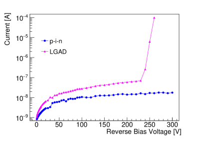
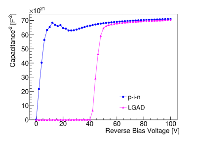
The LGAD being tested, along with the p-i-n detector used for comparison, was manufactured by Hamamatsu Photonics K.K. (HPK) [2], specified as HPK Type 3.1-50. The p-type bulk of the detectors has an active thickness of and a size of . Guard rings are distributed outside the active area. The I-V and C-V characteristics were measured under reverse bias, as shown in Figure 1(b). The experimental setup consisted of a Keithley 2410 power supply, a Keithley 6487 current meter, and an Agilent E4980A LCR meter operating at a frequency of .
The abrupt junction model has been used to estimate the distribution of doping. Both the p-i-n and LGAD structures exhibit a bulk doping concentration of . Additionally, the LGAD structure incorporates a deep-doped region with a concentration of , which is estimated from C-V data and the gain rate. The deep-doped area is specifically modeled within the LGAD structure, covering a range of .
2.2 Experiment Setup
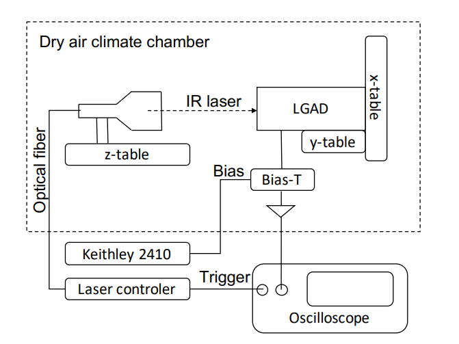
The experimental setup for the edge-TCT scan is illustrated in Figure 2. An infrared laser with a wavelength of 1064 nm is utilized, which has an attenuation length of approximately 1 mm in silicon. The given length is sufficient for the laser beam to effectively penetrate the detector. The beam waist of the pulse has a full width at half maximum (FWHM) measurement of 8 m, and the pulse duration is 350 ps. Denoting the direction of the laser beam as the -axis, the direction along the edge as the -axis, and the direction of the electric field inside the detector as the -axis serves as a convenient coordinate system for analysis. The value of z is initialized to zero at the top of the detector. The laser beam should be positioned perpendicular to the edge surface of the detector. Three portable tables have been arranged to facilitate the adjustment of the laser’s focal point, enabling a comprehensive z-scan across the entire thickness of the detector (0 to 50 m) with a step size of 1 m. Before capturing the laser-induced waveform, the laser beam is precisely directed towards the edge of the active area of the detector. This is achieved by adjusting the focus of the laser in a direction perpendicular to the laser beam at different positions along the z-axis. This ensures that the generated electron-hole pairs are within a restricted range near the designated value of . The resulting variation in waveform amplitude is then observed to determine the minimum width of the laser beam. A Keithley 2410 source is used as a high-voltage power supply. To enhance the signal, a CIVIDEC [4] wideband amplifier with a bandwidth of 2 GHz, a gain of 40 dB, and an integrated bias-Tee is utilized. After shaping, the signal was converted into a digital format and recorded using a Keysight DSO9254A oscilloscope [5], which has a bandwidth of 20 GHz and a sample rate of 20 GSa/s.
In the following TCT tests, the devices were measured at room temperature. Except for gain measurement, the devices were biased at 200 V from the backside.
3 Modeling
The modeling of the edge-TCT process can be categorized into four main components: field solution, generation of laser-induced non-equilibrium carriers, collection of carrier drift signals, and filtering of the final waveform. For LGAD, an additional step of carrier multiplication is implemented.
3.1 Field profile
The electric potential of a detector can be calculated by solving the Poisson equation
| (1) |
in which represents the vector coordinates, denotes the unit charge, denotes the dielectric constant of the detector material, and denotes the effective doping concentration. The depletion ansatz is used to simplify the calculation. In addition, it is assumed that the depletion area of the heavily-doped Ohmic contact layers is thin enough to be considered negligible.
The calculation of the weighting potential for signal generation is performed in a similar manner, using the following equation
| (2) |
At the readout electrode, is set to 1, while on all other electrodes, is set to 0.
Within regions of high electric fields, carriers undergo acceleration and gain enough energy to ionize electrons in the valence band. The multiplication behavior of carriers is determined by the ionization rate, which is defined as the number of electron-hole pairs generated by a drifting carrier as it travels a unit distance. The ionization rate for electrons () and holes (), which is determined by the temperature and intensity , can be expressed as [8]
| (3) |
where and are fixed parameters, and is a correction term for phonon-electron interaction, with and denoting the average phonon energy within the material [24].
3.2 Laser and carrier generation
The rate at which light-induced carriers are generated is proportional to the intensity of the laser beam. For a typical Gaussian laser beam in the direction, the light intensity distribution is [25]
| (4) |
where , and are the single pulse energy and the pulse duration of the laser, and are the beam widths at and (with the origin at the beam focus), determined by the numerical aperture () of the focusing lens and the laser wavelength (). The spatial FWHM of the laser beam is related to by .
Considering refraction and absorption, the intensity function will change its form into
| (5) |
The photons emitted by the laser beam are converted into excitation energy for the carriers. During a small time interval , the density of generated carriers can be calculated by
| (6) |
where represents the energy of a photon.
3.3 Carrier drift and multiplication
Once the carriers are excited, they will drift through the bulk material, thereby generating an electric current. According to the mobility formula [22]
| (7) |
the velocity of a carrier at a given position can be mathematically represented as a function of the effective doping concentration and the electric field intensity . In this study, the Reggiani model [9] is employed. Aside from oriented drifting, a Langevin term is considered to simulate the random motion of the carriers by adding a Gaussian displacement , the probability distribution function of which is
| (8) |
where
| (9) |
is the Einstein diffusion coefficient. Here, , , and refer to the Boltzmann constant, temperature, and elementary charge, respectively.
According to Shockley-Ramo’s theorem, a signal will be generated at the reading electrode during the drift of a charge by
| (10) |
The complete signal waveform can be acquired by combining the signals from all generated carriers. Additionally, in LGAD, a carrier in the gain layer induces carrier multiplication, which leads to signal amplification.
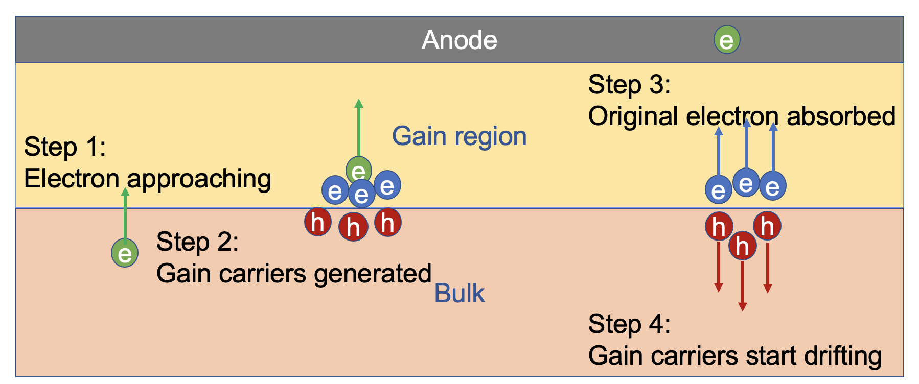
Instead of simulating the avalanche step by step, as illustrated in Figure 3, it is assumed that the entry of a single carrier into the gain layer will result in the generation of pairs of carriers without ionizing capability at the bottom of the gain layer, where
| (11) |
is the gain factor of the device [22]. As the values of and are sufficiently small outside the designated gain layer, it is advantageous to only integrate within the gain layer, which has a width of . The integral diverges when the device breaks down. For the LGAD under test, the value of is determined to be 23.4.
Due to the double-exponential relationship between the field intensity and the parameter (see Eq. 3 and 11), even a minor modification in the doping profile can result in a substantial change in the gain rate. This statement elucidates the challenges associated with the fabrication process of LGAD. However, in simulation, it is possible to make a numerical adjustment to the doping profile (by ) in order to align the gain rate value with experimental results.
3.4 Signal collection
Amplification is needed for the original induced currents to be detected, stored, and analyzed. The electronic system can be modeled as shown in Figure 4, which incorporates the signal effects of various devices. These effects include the capacitance and the AC resistance of the detector. Additionally, the inductance and capacitance of the bias-tee contribute to these effects. Furthermore, the gain () of the amplifier, the input resistance (), the output resistance (), and the capacitance of the cable () also contribute to these effects.
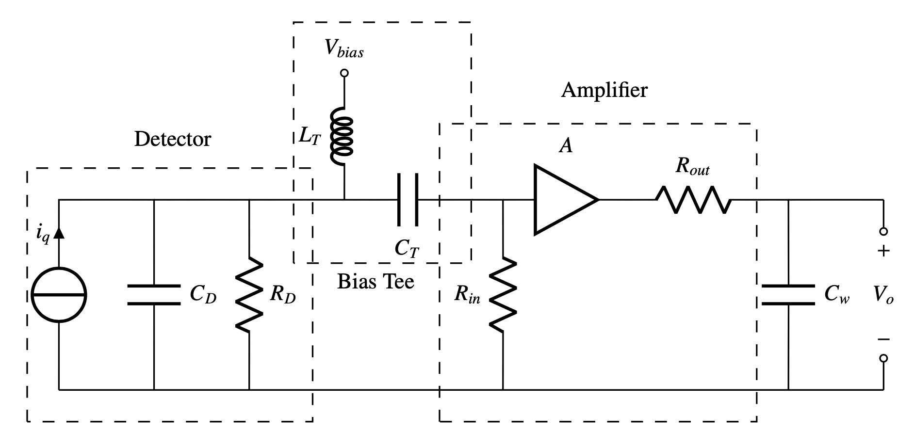
In the frequency domain, if and are small enough to be neglected, the transfer function of the aforementioned devices can be expressed as (letting )
| (12) |
and by using Laplace transformation, the amplification and shaping of the original signal can be expressed through convolution with
| (13) |
where and are the time constants of the circuit. Additionally, is the total amplification rate, measured in units of , that converts the original current signal into voltage.
4 Waveform Simulation
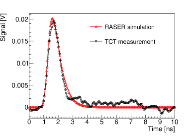
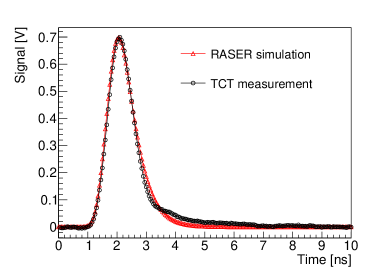
This section aims to evaluate the results of the edge-TCT z-scan in the direction of the device thickness. A global normalization factor is applied to both p-i-n and LGAD. For LGAD, the laser intensity is 0.58 times stronger than that of p-i-n in order to obtain a more distinct waveform.
In Figure 5, a good match of waveforms is exhibited when comparing the simulation and experimental results of p-i-n and LGAD. But to ensure reliable edge-TCT scan simulation, the waveform quantities, such as amplitude, rise time, and charge collection efficiency, should have a good agreement with experimental results at every point.
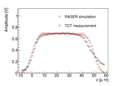
4.1 Amplitude
Figure 6(a) illustrates the relationship between the amplitude () of the waveform and the position of the laser focus (). The simulation results demonstrate an overestimation in the range of and an underestimation in the range of . This phenomenon may potentially be attributed to the diffusion of dopants inside the substrate, resulting in a non-abrupt junction between the substrate and the bulk. Additionally, the lack of consideration for light-induced carriers within the substrate, which diffuse into the active layer, may have also played a role.
4.2 Rise time
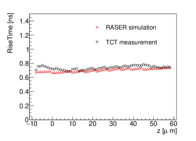
The rise time of a signal can be determined by performing linear fitting on the data points within the range of 20% to 80% of the signal’s amplitude. The relationship between the rise time and the variable is illustrated in Figure 6(b). An uniform result of 0.7 ns is observed and simulated for LGAD, indicating stable signal generation and an excellent signal-to-noise ratio. The presence of jaggedness within the figure can be attributed to the use of discrete data points.
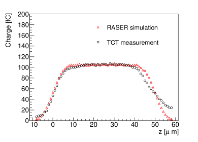
4.3 Charge collection
In this work, the charge collection of a waveform is defined as the integral of the current over a specific time period. The result of the charge versus focus coordinate is shown in Figure 6(c). As mentioned in Section 4.1, apart from the junction and carrier diffusion at the bottom, the charge collection successfully reflected the deposition of laser energy.
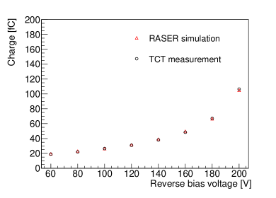
4.4 Gain measurement
To measure the gain rate of LGAD, we examined the relationship between charge and reverse bias voltage . Figure 6(d), which was sampled at . No charge collection change is observed for p-i-n, thus the charge collection of p-i-n is used as a contract. Under the given voltage range of , the gain rate of LGAD increases from 4 to 26. At 200V, the integral in 11 is 23.4, while the simulation result from the waveform is 24, with a relative error of less than 10%.
With comparisons of several quantities, an edge-TCT z-scan of silicon LGAD is performed to ensure the accuracy of LGAD simulation. This work solidifies and enhances the method of simplifying multiplication, making it more reliable. It serves as a foundation for future research.
5 Electric Field Measurement
5.1 Velocity profile
The primary utility of edge-TCT lies in its ability to quantify the electric field within the bulk of the detectors. The velocity profile method is widely employed, particularly for p-i-n detectors [11]. For an electron or hole moving within the interior of the detector’s active area, its velocity is determined by the field intensity, as described by Equation 7. The signal, which is primarily determined by the drifting velocity (excluding trap capture), can be expressed using Equation 10. That is, it has the capability to extract field intensity information from the edge-TCT waveform.
Considering a pair of carriers generated at a specific location , the sum of their velocities at the instant they are generated is
| (14) | ||||
If a group of carriers conforms to the assumption that they are produced within a limited region and time period around , then the resulting signal they generate should be
| (15) |
as , and in planar structure detectors. After amplification and RC shaping, it can be observed that this proportional relationship may not hold strictly true. However, the functional relationship should remain valid.
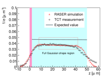
To counteract the effect of carriers leaving the laser focus and carriers emerging, the velocity profile is chosen as the signal value 0.1 ns after the waveform emerges. The simulation results of the LGAD, as depicted in Figure 7, demonstrate a significant peak at for the simulation and for the experiment. Both results show no correlation with the known theoretical LGAD field. The velocity profile method actually loses its effectiveness for LGAD with our facilities.
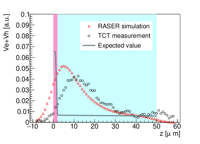
This could actually be proven by the analyses provided below. According to Equation 15, the extracted signal, denoted as , should exclude the gain signal. However, it is not possible to distinguish between the peak of laser intensity and the peak of the gain signal (see Figure 5(b)). To provide a more precise and comprehensive explanation, in systems where the time required for carrier drifting is roughly equivalent to the duration of the laser pulse (both of which are approximately 0.5 ns in our facilities), the ”velocity profile” does not provide any information about the coordinates of the focal point. Consequently, it is not suitable for quantifying velocity or field intensity. Additionally, the back-end electronics may also impact the resolution. For systems of this nature, a specific methodology is required to analyze the internal built-in field, using additional variables. In addition to considering the idealized signal input, an alternative approach involves examining the collective behavior of non-equilibrium carriers induced by light and analyzing their statistical behavior.
5.2 Diffusion Profile
In this section, the width of the propagating carrier cluster is being researched. Ignoring carrier recombination, the distribution of a cluster of light-induced non-equilibrium carriers drifting and diffusing under a uniform electric field is [24]
| (16) |
where , represents the initial distribution of the carriers as defined in equation 5, and if the diffusion coefficient is constant. The convolution is performed in both the spatial and temporal dimensions.
For an initial spatial-temporal Gaussian distribution with spatial spread and temporal spread , the convolution can be reduced to a variance composition as
| (17) | ||||
where represents the total number of carriers, denotes the temporal attenuation coefficient of the laser, , and represents the standard deviation of the initial Gaussian distribution of carriers. The convolution asterisk now only affects the time dimension. This analysis is effective for edge-TCT, as the injected Gaussian beam profile behaves like a Gaussian function with and .
Now consider the elongation of the carrier cluster during drifting. Denote and as the diffusion constant and the field intensity at the center of the carrier cluster, respectively. In an infinitesimal time period , the distance between any two carriers would be stretched by the gradient of the field, which can be represented as . Additionally, the Einstein coefficient will change as the carrier cluster center moves, and as a result, the overall distribution will take this form:
| (18) |
Therefore,
| (19) |
Thus, we could integrate (the foot marks and represent the initial and end points of the cluster center’s path) and obtain
| (20) |
and if the variation of mobility could be ignored and a uniformly doped bulk is considered (the electric field intensity of which could be calculated by ), it is revealed that
| (21) |
where .
Now consider the multiplication process in LGAD. Notice that from then on, only the carriers leading the avalanche will be considered, as due to the device design, they often have a larger ionization rate. To simplify calculations, it could be assumed that during the avalanche, the diffusion speed of the carrier cluster is slow enough for the spatial distribution to be treated as Gaussian with a variance that does not change over time. Thus, to count the carriers that reached the gain layer from a given cluster, the relation 17 can be deduced into
| (22) |
where refers to the bottom of the gain layer, represents the drifting velocity of the carriers at that location, and .
Consider carriers, the number of which is , passing through the gain layer within a small time period . As a result, ionized carrier pairs are created, which then start to drift and generate a signal. As only carriers with opposite charges can continue to drift and contribute to the signal while crossing the space charge region, the amplitude will increase by (where the prime denotes carriers with a different charge sign, and represents the thickness of the detector). Therefore, the time derivative of the total gain signal, , is proportional to , and the maximum of the derivative is also proportional to the maximum of . This is because the gain signal dominates the rising edge of the total signal by
| (23) |
where Notice that for non-irradiated detectors, could be completely determined by the wavelength of the laser and properties of the detector, since is a function of , and the value of can be estimated by where and represent the full depletion voltages of the gain layer and the active area.
Considering the distribution of edge-TCT induced carriers described by Equation 4, in Equation 20 or 21, will be replaced by the beam waist . Additionally, it is necessary to integrate along the laser beam direction in order to evaluate the change in beam waist. Plus, to account for attenuation from Equation 5, within the range , the total number of carriers is . Thus,
| (24) |
For facilities utilized in this work, since is a relatively large term (approximately 15 ) and is less than 1.1, the result should be approximately constant. Though, we could expect the diffusion profile method to be more valuable and provide more information in the case that is relatively small.
The simulated and experimental diffusion profiles of LGAD are shown in Figure 7(b), along with the corresponding theoretical values. The reliability of the diffusion profile method for LGAD has been proven, as it accurately predicts and observes absolute results.
6 Conclusion
The present study has successfully established and tested the diffusion profile method for measuring the bulk field in LGAD (low-gain avalanche detector). This methodology aims to use thin detectors with a thickness approximately ten times the FWHM (full width at half maximum) of the laser beam. By calculating the temporal derivative of the waveform, valuable information about the diffusion process can be obtained, as well as its impact on the flattening of the carrier cluster. The methodology is expected to yield immediate results by using directly measurable parameters, eliminating the need for normalization.
This study effectively conducted a simulation of the edge-TCT (edge transient current technique) on non-irradiated silicon LGAD using the particle detector simulation package RASER. The simulated waveform was used to fit the data. Subsequently, an edge-TCT scan was generated by comparing the experimental results with HPK Type 3.1 detectors (p-i-n and LGAD) to determine its reliability. The comparison yielded successful results in terms of amplitudes, rise times, and charge collections, thereby confirming the accuracy of the simulation in edge-TCT.
A comparable simulation procedure could be implemented to examine the performance of detectors made from alternative materials, such as silicon carbide, with a specific focus on their resistance to radiation when exposed to a particular irradiation flux. Based on prior research [7], simulation can also be used to investigate TCT tests on detectors with non-planar structures [32].
Acknowledgement
This work has been supported by the China Postdoctoral Science Foundation (No. 2022M710085), the State Key Laboratory of Particle Detection and Electronics (No. SKLPDE-KF-202313), and the Natural Science Foundation of Shandong Province Youth Fund (No. ZR202111120161). We have completed this work as part of the CERN RD50 collaboration framework, with the experiment conducted at the CERN-SSD laboratory. We would like to thank Marcos Fernández García and Michael Moll for their support during the experiment, as well as the TRACS team for their valuable cooperation and discussions.
References
- [1] X. Shi et al., “raser · PyPI,” https://pypi.org/project/raser/, [accessed June 25, 2023].
- [2] H. P. K.K., https://www.hamamatsu.com, [accessed June 25, 2023].
- [3] M. Moll et al., “CERN RD50 - Radiation hard semiconductor devices for very high luminosity colliders,” https://rd50.web.cern.ch, [accessed June 25, 2023].
- [4] CIVIDEC, “cividec instrumentation - CVD Diamond Technology applications,” https://cividec.at/electronics-C2-HV.html, [accessed June 25, 2023].
- [5] KEYSIGHT, “DSO9254A Oscilloscope: 2.5 GHz, 4 Analog Channels [Discontinued] — Keysight,” https://www.keysight.com/us/en/product/DSO9254A/oscilloscope-2-5ghz-4-analog-channels.html, [accessed July 16, 2023].
- [6] T. Yang et al., “Time Resolution of the 4H-SiC PIN Detector,” Frontiers in Physics, vol. 10, 2022. [Online]. Available: https://www.frontiersin.org/articles/10.3389/fphy.2022.718071
- [7] Y. Tan et al., “Timing Performance Simulation for 3D 4H-SiC Detector,” Micromachines, vol. 13, no. 1, 2022. [Online]. Available: https://www.mdpi.com/2072-666X/13/1/46
- [8] R. Van Overstraeten and H. De Man, “Measurement of the ionization rates in diffused silicon p-n junctions,” Solid-State Electronics, vol. 13, no. 5, pp. 583–608, 1970. [Online]. Available: https://www.sciencedirect.com/science/article/pii/0038110170901395
- [9] S. Reggiani, M. Valdinoci, L. Colalongo, M. Rudan, G. Baccarani, A. D. Stricker, F. Illien, N. Felber, W. Fichtner, and L. Zullino, “Electron and hole mobility in silicon at large operating temperatures. i. bulk mobility,” IEEE Transactions on Electron devices, vol. 49, no. 3, pp. 490–499, 2002.
- [10] G. Kramberger et al., “Investigation of Irradiated Silicon Detectors by Edge-TCT,” IEEE Transactions on Nuclear Science, vol. 57, no. 4, pp. 2294–2302, 2010.
- [11] ——, “Electric field modeling in heavily irradiated silicon detectors based on Edge-TCT measurements. ”Why p-type is Better than n-type” or Electric Field in Heavily Irradiated Silicon Detectors,” PoS, vol. Vertex2012, p. 022, 2013. [Online]. Available: https://cds.cern.ch/record/2634361
- [12] B. Schmidt, “The high-luminosity upgrade of the LHC: Physics and technology challenges for the accelerator and the experiments,” Journal of Physics: Conference Series, vol. 706, no. 2, p. 022002, apr 2016. [Online]. Available: https://dx.doi.org/10.1088/1742-6596/706/2/022002
- [13] V. Izzo, “ATLAS Upgrades,” CERN, Geneva, Tech. Rep., 2021. [Online]. Available: https://cds.cern.ch/record/2732959
- [14] R. Longo, “Joint ATLAS/CMS ZDC upgrade project for the High Luminosity LHC,” CERN, Geneva, Tech. Rep., 2022. [Online]. Available: https://cds.cern.ch/record/2825363
- [15] L. Soffi, “Physics opportunities with a MIP Timing Detector in CMS at HL-LHC,” CERN, Geneva, Tech. Rep., 2022. [Online]. Available: https://cds.cern.ch/record/2840966
- [16] G. Calderini, “The ATLAS ITk detector for High Luminosity LHC upgrade,” Nuclear Instruments and Methods in Physics Research Section A: Accelerators, Spectrometers, Detectors and Associated Equipment, vol. 1040, p. 167048, 2022. [Online]. Available: https://www.sciencedirect.com/science/article/pii/S0168900222004715
- [17] H. F. W. Sadrozinski et al., “Sensors for ultra-fast silicon detectors,” Nucl. Instrum. Methods A, vol. 765, pp. 7–11, 2014. [Online]. Available: http://dx.doi.org/10.1016/j.nima.2014.05.006
- [18] Z. Galloway et al., “Properties of HPK UFSD after neutron irradiation up to 6e15 n/cm2,” Nuclear Instruments and Methods in Physics Research Section A: Accelerators, Spectrometers, Detectors and Associated Equipment, vol. 940, pp. 19–29, 2019. [Online]. Available: https://www.sciencedirect.com/science/article/pii/S0168900219306278
- [19] X. Yang et al., “Layout and performance of HPK prototype LGAD sensors for the High-Granularity Timing Detector,” Nuclear Instruments and Methods in Physics Research Section A: Accelerators, Spectrometers, Detectors and Associated Equipment, vol. 980, p. 164379, 2020. [Online]. Available: https://www.sciencedirect.com/science/article/pii/S0168900220307762
- [20] G. Giacomini et al., “Fabrication of Different LGAD-Based Devices at BNL,” in 2021 IEEE Nuclear Science Symposium and Medical Imaging Conference (NSS/MIC), 2021, pp. 1–4.
- [21] M. O. Wiehe, “Development of a two-photon absorption - tct system and study of radiation damage in silicon detectors,” Ph.D. dissertation, Freiburg U., Freiburg U., 2021.
- [22] B. J. Baliga, Fundamentals of Power Semiconductor Devices. Springer, 2019.
- [23] J. Calvo et al., “TRACS: A multi-thread transient current simulator for micro strips and pad detectors,” Nuclear Instruments and Methods in Physics Research Section A: Accelerators, Spectrometers, Detectors and Associated Equipment, vol. 917, pp. 77–85, 2019. [Online]. Available: https://www.sciencedirect.com/science/article/pii/S0168900218317856
- [24] K. Seeger, Semiconductor physics: An introduction. Springer, 2011.
- [25] K. Thyagarajan and A. Ghatak, Lasers: Fundamentals and Applications, ser. Graduate Texts in Physics. Springer US, 2010. [Online]. Available: https://books.google.com.hk/books?id=z13wEOBwn1wC
- [26] S. Spannagel et al., “Allpix Squared - Generic Pixel Detector Simulation Framework,” https://doi.org/10.5281/zenodo.6387859, [accessed June 25, 2023].
- [27] F. Cenna et al., “Weightfield2: A fast simulator for silicon and diamond solid state detector,” Nuclear Instruments and Methods in Physics Research Section A: Accelerators, Spectrometers, Detectors and Associated Equipment, vol. 796, pp. 149–153, 2015, proceedings of the 10th International Conference on Radiation Effects on Semiconductor Materials Detectors and Devices. [Online]. Available: https://www.sciencedirect.com/science/article/pii/S0168900215004842
- [28] M. S. Alnaes et al., “The FEniCS project version 1.5,” Archive of Numerical Software, vol. 3, 2015.
- [29] V. Eremin et al., “Development of transient current and charge techniques for the measurement of effective net concentration of ionized charges (Neff) in the space charge region of p-n junction detectors,” Nuclear Instruments and Methods in Physics Research Section A: Accelerators, Spectrometers, Detectors and Associated Equipment, vol. 372, no. 3, pp. 388–398, 1996. [Online]. Available: https://www.sciencedirect.com/science/article/pii/0168900295012958
- [30] N. Moffat et al., “Low Gain Avalanche Detectors (LGAD) for particle physics and synchrotron applications,” Journal of Instrumentation, vol. 13, no. 03, p. C03014, mar 2018. [Online]. Available: https://dx.doi.org/10.1088/1748-0221/13/03/C03014
- [31] V. Eremin et al., “The origin of double peak electric field distribution in heavily irradiated silicon detectors,” Nuclear Instruments and Methods in Physics Research Section A: Accelerators, Spectrometers, Detectors and Associated Equipment, vol. 476, no. 3, pp. 556–564, 2002, proc. of the 3rd Int. Conf. on Radiation Effects on Semiconductor Materials, Detectors and Devices. [Online]. Available: https://www.sciencedirect.com/science/article/pii/S0168900201016424
- [32] L. Diehl et al., “Comparison of the time resolution of unirradiated and irradiated LGADs and 3D sensors,” Nuclear Instruments and Methods in Physics Research Section A: Accelerators, Spectrometers, Detectors and Associated Equipment, vol. 1046, p. 167691, 2023. [Online]. Available: https://www.sciencedirect.com/science/article/pii/S0168900222009834
- [33] S. Selberherr et al., “The evolution of the MINIMOS mobility model,” Solid-State Electronics, vol. 33, no. 11, pp. 1425–1436, 1990. [Online]. Available: https://www.sciencedirect.com/science/article/pii/003811019090117W