Gate-defined Josephson weak-links in monolayer WTe2
Abstract
Systems combining superconductors with topological insulators offer a platform for the study of Majorana bound states and a possible route to realize fault tolerant topological quantum computation. Among the systems being considered in this field, monolayers of tungsten ditelluride (WTe2) have a rare combination of properties. Notably, it has been demonstrated to be a Quantum Spin Hall Insulator (QSHI) and can easily be gated into a superconducting state. We report measurements on gate-defined Josephson weak-link devices fabricated using monolayer WTe2. It is found that consideration of the two dimensional superconducting leads are critical in the interpretation of magnetic interference in the resulting junctions. The reported fabrication procedures suggest a facile way to produce further devices from this technically challenging material and the results mark the first step toward realizing versatile all-in-one topological Josephson weak-links using monolayer WTe2.
I Introduction
A two-dimensional (2D) topological insulator or Quantum Spin Hall Insulator (QSHI) exhibits a bulk energy gap that is created due to a particular crossing of bands near the Fermi level (band inversion) which can then interact through spin-orbit coupling. The arrangement of bands in this scenario can be represented by the nontrivial topology, an implication of which are the existence of one-dimensional, conducting edge states that accompany the typical bulk spectrum1, 2, 3, 4. These edge states are helical (exhibit spin-momentum locking) and thus are robust to elastic scattering, implying ballistic transport and the observation of a quantized conductance (), where is the number of edge channels. The original proposal for a QSHI concerned the opening of a spin-gap in the 2D material graphene due to the spin-orbit interaction3, 4. However, graphene’s intrinsic spin-orbit interaction was found to be too weak to enable observation of the QSHI state experimentally. Recently graphene/ and graphene/ heterostructures have been studied as a route toward enhancing the spin-orbit interaction5, increasing the effective spin gap to make the QSHI state experimentally accessible. One class of 2D materials, the transition metal dichalcogenides (TMDs), present another promising path toward identifying QSHI materials. They possess a number of polytypic crystal phases (2H, 1T, and 1T’) and are predicted to exhibit a QSHI state if the structure is in the monoclinic 1T’-phase6. Among TMDs, the monolayer tungsten ditelluride () is predicted to stably exist within the 1T’-phase, making it a suitable system for the study of a 2D crystalline QSHI. A number of experimental studies have identified strong evidence for the QSHI state in monolayer through conductance quantization7, 8, 9, 10, 11, scanning tunnelling microscopy measurements12, 13, 14, and direct observation of edge states through scanning microwave impedance spectroscopy15. Strikingly, it has also been demonstrated that monolayer WTe2 can host an intrinsic superconducting phase by means of gate-induced electrostatic tuning16, 17. Such behavior is also reported in twisted bilayer graphene18, where surface gates have been used to form Josephson weak-links and tune the system through a complex phase space19, 20, 21. The coexistence of superconductivity and intrinsic topological states in WTe2 makes it an ideal platform to study Majorana zero modes in a single material system by gate-definition of a Josephson weak-link.
Josephson weak-links created by interfacing a QSHI with an s-wave superconductor are predicted to host Majorana modes, as proposed in the seminal work of Fu and Kane22, 23. In combination with device designs to break time-reversal symmetry in the edge states (via local gating or ferromagnetic materials) such a system can be a platform to study localized Majorana Fermions, which have applications in topological quantum computing24, 25, 26, 27, with realistic proposals for the design for topological qubits28. A number of QSHI systems have been studied in combination with superconductors to probe the presence of topological superconducting states with efforts in the based system29, 30, 31 and the system32, 33. Reports of planar weak-links using 2D materials are surprisingly uncommon and they are almost exclusively fabricated using graphene34, 35, 36, 37, 38, 19, 20, 21, with other recent reports using black phosphorus monolayers39 and efforts using 40, 41. To our knowledge, there are no reports of such devices made with a 2D crystal QSHI. The ability of monolayer WTe2 to be tuned from the QSHI to superconducting state suggests a clear path toward realizing a planar Josephson weak-link in a single material where the superconducting and QSHI elements are explicitly defined by gates16, 17. Despite this and the not-so-recent prediction of that WTe2 may host topological states6, 42, no Josephson weak-link devices have been reported with the monolayer material to date. The primary reason is that few- and monolayer is challenging to process into devices due to the rapid oxidization of its surface under ambient conditions43, 44, 45, 46, 47 and even in a high purity environment48. Oxidation effectively destroys the monolayer material and severely impedes the transport properties of multilayers, for example, by greatly suppressing its magnetoresistance49, 44. Therefore, fabrication must be performed quickly and adapted to inert gas (e.g. argon) environments.
In this report, we present the fabrication and measurement of gate-defined Josephson weak-link devices with encapsulated monolayer . Contacts to the encapsulated are formed using an edge contacting technique, utilizing in-situ reactive ion etching of the stack followed by dc-sputter deposition of superconducting contacts, which provides superconducting connections to the external device circuit. Device contacts are formed using a thin contacting layer of sputtered Pd, motivated by recent reports50, 51, 52 of induced superconductivity in multilayer through diffusion of forming regions of . The clean Pd/WTe2 interface is found to produce good superconducting contacts upon the annealing of the system in later processing steps (see Supplementary Note 1). The channel of the device is defined by electrostatic gates which can locally drive sections of the monolayer superconducting, creating a Josephson weak-link, in which the layer forming the weak-link is monolayer . We demonstrate that electrostatic gating can induce a superconducting state in the system (sections 2.1 and 2.2) and then confirm the presence of a Josephson weak-link through measurements of the magnetic response and the Shapiro response (inverse ac-Josephson effect). We report measurements on a single device in the main text alongside complementary measurements of a second device in supplementary Note 2a.
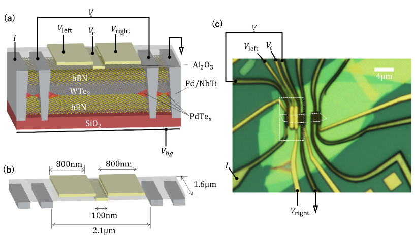
A schematic of the device design and optical image is shown in figure 1. The device studied consists of a channel with three surface-gates. Namely, a narrow center gate () on the capping hBN and a pair of wider gates ( and ), isolated from using a layer of grown by atomic layer deposition. These terminals facilitate gating of the underlying into the superconducting state. The edge contacts span the width of the flake. Measurements taken between the contact pairs used for source or drain terminals reveal supercurrent and only a weak gate response, so we conclude that the processing has resulted in diffusion of forming and effectively shorting the contacts (Supplementary Note 1). In contrast, the device channel resides far beyond the distance anticipated for the diffusion and reveals the strong gate response indicative of the monolayer . Fabrication details are given in methods section 4.1.
II Results and discussion
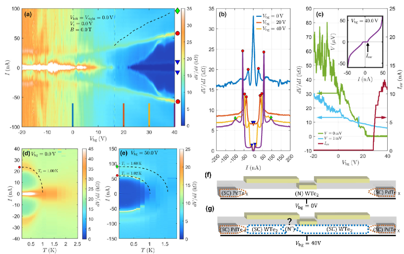
II.1 Josephson weak-link in monolayer WTe2 formed by a global back-gate
Before discussing the situation in which the channel is explicitly defined by local gates, we initially demonstrate that the device can exhibit superconducting transport when a positive bias is applied to the global back-gate () which acts through nm of thermally grown on the silicon substrate. In figure 2 (a), we present a color plot of the differential resistance () as a function of both applied current () and back-gate voltage (). Figure 2 (b) then shows cross-sections of this plot at selected values of . For V, the chemical potential of the monolayer is sitting near or within the gap such that its contribution to the transport is nearly insulating. Conversely, the contacts are far below their and superconducting. In this case, we effectively produce an S-N-S junction (figure 2 (f)). In the corresponding trace of as a function of in figure 2 (b), we observe a sharp resistance peak at zero current flanked by a pair of smaller satellite peaks at nA (red circles). The zero current feature can be qualitatively understood through the scattering dynamics of normal electrons and quasiparticles at a low transparency S-N-S interface. In the context of BTK theory53, 54, 55, one expects for a very low transparency junction a suppressed current within the bias window of the superconducting gap due to the greater influence of normal reflections as opposed to Andreev reflections. Consistent with this scenario, the satellite peaks arise from the superconducting regions transitioning to the normal state at a critical current of nA. Indeed, temperature dependent measurements of these peaks reveal a BCS-like dependence (figure 2 (d)) with an associated K. At higher currents, all elements of the system are normal and the net resistance stabilizes to a constant value near .
For V, the system is significantly doped such that the monolayer undergoes a transition to a superconducting state. Consequently, several new features appear in the transport. The first of which is a narrow supercurrent branch about zero bias with associated resistance peaks at nA (blue triangles). We attribute these features to the formation of a Josephson weak-link somewhere within the device channel (figure 2 (g)). In this scenario, the peaks (blue triangles) correspond to the switching current () of the junction, which we define as the maximum supercurrent that the junction can support before transitioning or switching to the dissipative transport branch (as shown in the inset of figure 2 (c)). The formation of a weak-link is corroborated by observation of interference patterns in the magnetic response (presented in section 2.4) and observation of a Shapiro response (section 2.3). The origin of the weak-link may be a region of normal or a micro-constriction within the monolayer which is driven normal by transport current. Accordingly, we denote the weak-link as S-N’-S. Possible origins will be discussed in further detail in section 2.5. At higher currents, we observe that the resistance peaks associated with the critical current of the superconducting (red circles) shift to higher currents ( at V) and then finally a new pair of weak resistance maxima (green diamonds) appear. We associate these features with the superconducting gap of the monolayer, as they appear approximately constant in bias (Supplementary Note 3). This interpretation is consistent with temperature dependent measurements (figure 2 (e)), which again reveal a BCS-like dependence of each feature, with the having (K) and the monolayer having (K). We note that these critical temperatures differ from reported values in the literature50, 51, 52, but the results are consistent with a secondary monolayer device in which was estimated in a different manner (Supplementary Note 2b). Finally, we conjecture that the V data represents a transitive state in which a Josephson weak-link has formed, but cannot yet support a supercurrent due to poor transparency. The explicit effect of on device resistance and the observation of supercurrent is shown in figure 2 (c). For example, the orange trace indicates that a switching current can be observed at V. The small critical current associated with the (indicated with red circles in all plots) complicates the analysis of features in the dissipative transport beyond the supercurrent branch because when it becomes normal, the junction bias is now dropped across not only the weak-link, but also the contacting regions. See Supplementary Note 3 for plots of transport features as a function of voltage. In addition to those already discussed we note an additional transport feature that emerges between the supercurrent branch (blue triangles) and the transition associated with the (red circles), appearing around and merging with the feature near . The origin of this feature is inconclusive but its scaling in gate suggests that it originates in the gated superconducting regime and so could be a sub-gap transport feature associated with the weak-link such as resonances due to multi-Andreev reflections56 or possibly a region of the gated exhibiting a lower critical current.
II.2 Tunability of a gate-defined Josephson weak-link in monolayer
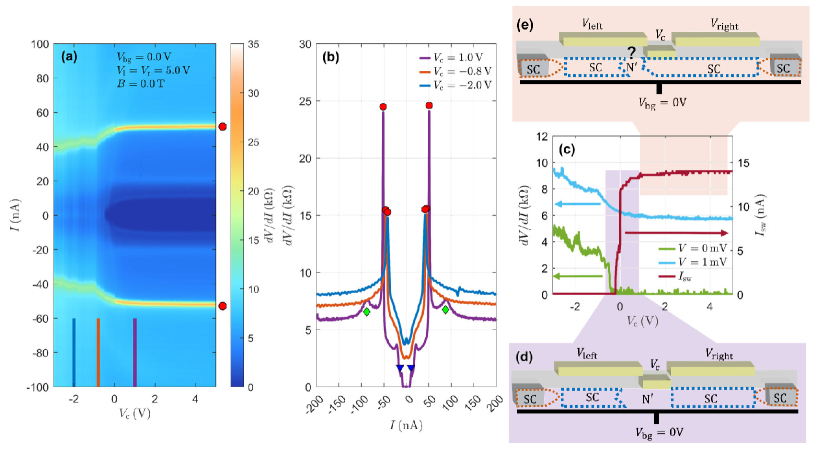
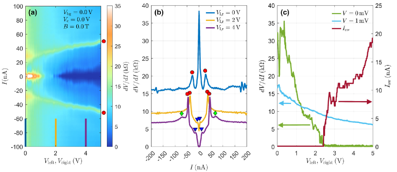
We now demonstrate that the as-patterned top-gates (, ) can perform a similar function as the global back-gate. In the present discussion, the formed Josephson weak-link is defined as a channel between the gated regions in a more deterministic manner, which is in contrast to the previous discussion where the weak-link’s position is not explicitly known. Furthermore, we will demonstrate that a patterned center gate () can turn on and off the supercurrent branch of the junction. The color plot of figure 3 (a) and its corresponding cross-sections (figure 3 (b)) should be compared to the equivalent panels of figure 2. We find that for increasing (, ) the device’s transport features (identified by colored symbols in figure 3 (b)) qualitatively mimic the progression discussed previously for the back-gated junction. This indicates that through local electrostatic gating, we are able to locally drive sections of the monolayer superconducting and create a Josephson weak-link in the central region (figure 4 (d)). Figure 3 (c) indicates that supercurrent can be observed at (, V). Here again we find properties of a Josephson S-N’-S weak-link, where we believe that the region is in close proximity to the center gate. We corroborate this point by demonstrating the tunability of this junction by . Figure 4 (a-c) illustrates the behavior of the device when (, V), a value high enough to induce superconductivity in the monolayer, and is changed to progressively more negative values. In figure 4 (a-b) it is observed that the channel supercurrent can be suppressed and for the highest negative , a resistance maximum near zero bias begins to form, confirming the expected behavior of an S-N-S junction without supercurrent. The proposed system behavior when a weak-link is formed is illustrated in figure 4 (d) and (e). For high values of the center gate region is superconducting but still some region of the device forms a S-N’-S weak-link (figure 4 (e)) as was seen in the back-gate induced superconducting case in figure 2. Here the influence of is saturated as the region of the device forming the junction is elsewhere. For low the center gate region is driven normal and the properties of the weak-link are tuned, figure 4 (e).
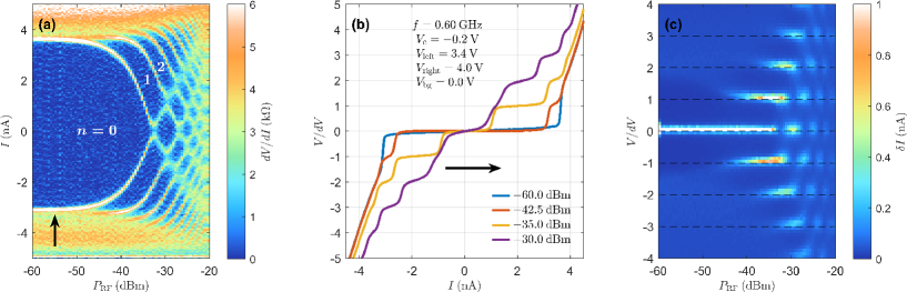
II.3 Shapiro response of the gate-defined weak-link
We demonstrate the properties of the gate-defined Josephson weak-link by measuring the response of the device to a microwave drive (figure 5). In a conventional Josephson weak-link, with sinusoidal current phase relationship , steps appear quantized in voltage at multiples of . With increasing ac-current amplitude the step widths in current exhibit an oscillating Bessel function like pattern57. The oscillatory pattern and good quantization of steps at voltages , are easily visualized by plotting histograms of binned measurement voltage data as shown in figure 5 (b). We observe conventional patterns with no evidence of sub-harmonic steps to indicate a non-sinusoidal current phase relationship58, 59. We also see no evidence of doubling of step voltages due to the fractional ac-Josephson effect associated with topological modes60, 31, 30. Additional Shapiro response data for a collection of alternative gating conditions can be found in Supplementary Note 7. Broadly, we observe that the visibility of the Shapiro steps scales with the weak-link .
II.4 Magnetic field response and asymmetric current distribution
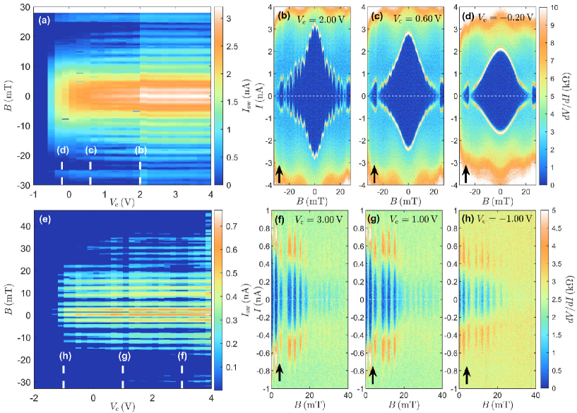
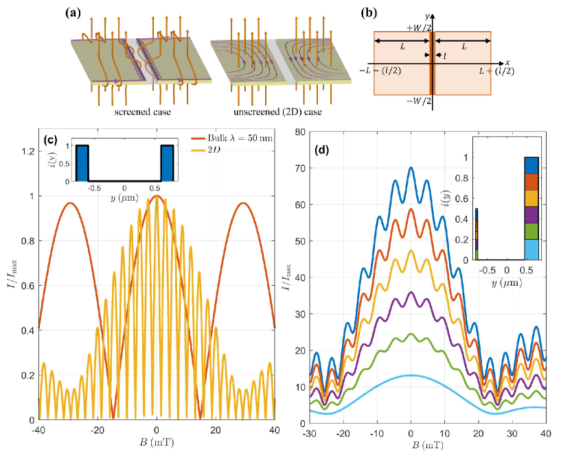
Additional confirmation of a weak link can be seen in the response of the junction to an out-of-plane magnetic field (). Figure 6 shows evaluated junction switching currents () as a function of and for the two different gating conditions. Explicitly, figure 6 (a-d) show the response for the superconducting state induced using and , while figure 6 (e-h) show the response with superconductivity induced using . Figure 6 (b-d) show differential resistance plotted as a function of for a range of different values of . For high (figure 6 (b)) we observe a Fraunhofer-like background decorated with small SQUID-like oscillations that are periodic in flux with a short period (mT). As is reduced, the visibility of the SQUID-like oscillations is diminished until only the background remains (figure 6 (d)). Figure 6 (f-h) show a similar set of traces for the back-gated case (without bias on and ). Note that here the values of are suppressed as compared to the measurement data presented in section 2.1 as a consequence of the measurement being performed at a later date after application of high fields to the sample and thermal cycling. Similar SQUID-like oscillations with a slightly longer period (mT) are observed and can be used to tune and eventually fully suppress the non-dissipative current (for additional data see Supplementary Note 4a). The period of the SQUID-like oscillations under both gate conditions is small ( - 2.4 mT), which is significantly below the field required to apply a flux quantum to the junction area defined by the gate of nominally . The short period of oscillations in is a consequence of the 2D nature of the gated superconducting regions that define the junction and can be understood in terms of the Pearl theory. In thin superconductors with film thickness () below the London penetration depth () the magnetic field screening is characterised by the Pearl length61 (). For thin 2D materials, the Pearl length may exceed the size of the sample leading to uniform penetration of magnetic flux throughout the unscreened device (figure 7 (a)). The uniform magnetic flux in this unscreened case causes modifications to the magnetic response of the junction as compared to more conventional systems with bulk leads in which flux only penetrates within the London penetration length around the lead perimeters due to screening. A Josephson junction with 2D superconducting leads thus has a magnetic interference pattern that is heavily influenced by the geometry of the leads themselves instead of the junction geometry itself. This can be visualized by the simulated response comparison plots of figure 7 (c). The effect of unscreened 2D superconductors has been observed in other 2D systems such as twisted bilayer graphene20, 19 and thin NbSe2 flakes62. SQUID-like oscillations with lifted or non-zero minima on a Fraunhofer-like background can have a range of origins, the simplest being an asymmetry in the current density profile63 across the junction giving rise to an asymmetric SQUID. We disregard any influence from self-screening currents and transparency (see Supplementary Notes 4d and 6a) and conclude that the observed magnetic response in the case of top-gate induced superconducting state is most likely due to such an asymmetry.
II.5 Simulation of the magnetic field response
To qualitatively study the magnetic field response under both gating conditions, we follow the work of Clem in [64] which describes a Josephson junction with rectangular leads which are smaller in dimensions than the Pearl length (see methods section 4.5). A rectangular geometry is well suited to our device layout assuming that the flake has an approximately uniform width. In figure 7 we show simulation results using parameters estimated for the device with m, m and nm (figure 7 (b)). In the simulations, we select current profiles which can qualitatively reproduce the magnetic response of the junctions formed using the different gating schemes. The behavior seen in the back-gated junction is similar to that seen for a symmetric current distribution concentrated about the edges of the sample (figure 7 (c)). Here, the influence of the SQUID-like features is strong and the minima have clearly defined zeros. As one tunes the asymmetry of the current distribution (figure 7 (d)), the coexistence of the SQUID-like and Fraunhofer-like features is still seen, but the relative strength of the SQUID-like features are softened as found in the magnetic response of the top-gated junction. To further evaluate a suitable current distribution describing the behavior of our device, we have utilized a minimization fitting approach following the work of Hui et al. in [65] (see Supplementary Note 5). Both approaches support the conclusion that inducing superconductivity with the back-gate results in a relatively symmetric current distribution across the junction width, with peaks in current near the channel edges. Conversely, when superconductivity is induced using the top-gates the current is predominantly carried in a peak located near one edge.
Under all gate conditions that we have studied we find that the system displays the properties of a weak-link formed somewhere within the device (as indicated with the magnetic and Shapiro response). We find that for some parameter range we are able to tune the system efficiently using the narrow center gate indicating that the weak-link is formed in proximity to the gate. The difference in current distributions for each gating condition could have several possible origins. The device as fabricated may possesses imperfections such as small bubbles after the stamping process which may lead to inhomogeneous gating and to more complex effective geometries. We speculate that such imperfections may be limiting the ability of one of the top-gates to tune part of the monolayer, leading to an effectively longer junction at one side of the flake. This would result in smaller critical currents along one edge and the observed asymmetric oscillations with a relatively longer . In contrast, the back-gate would be unaffected by this imperfection, which lies above the monolayer material. Furthermore the monolayer flake itself may possess a nontrivial geometry due to cracks either present before or produced following the stamping process, as have been observed in recent scanning microwave impedance measurements15, 11. Future devices may be improved through better pre-selection of materials for stacking and the use of graphite top and back-gates which have been demonstrated to improve gate disorder in graphene devices66. As we find no evidence to indicate series junctions being formed we believe that the center gate allows the tuning of the geometry of the N’ junction region. We note however that the geometry of the junction is challenging to evaluate from the magnetic response due to the unscreened nature of the 2D superconducting regions which causes phase to be accumulated both inside the weak-link and within the lead regions in a magnetic field (Supplementary Note 4b).
III Conclusions
We have fabricated and measured for the first time Josephson weak-links made from monolayer . Our approach involves electrostatic gating to define the various regions of the Josephson weak-link by utilizing the material’s recently reported ability to be tuned into the superconducting state. We confirm the Josephson effect through observation of a conventional Shapiro response and interference patterns in the weak-link’s magnetic response. In both back-gated and top-gated configurations, we observe SQUID-like oscillations in the magnetic field response, whose relative strength is tuned by application of the gate on the weak-link. Our analysis indicates that the majority of current is carried along states situated at the edges of the junction in the back-gated case, while current is carried predominantly along one edge in the top-gated case. Whether these observations are related to the expected topological edge states or simply imperfections in the channel formed during fabrication cannot be discerned. Our results highlight the experimental difficulty of realizing and measuring the predicted topological character of monolayer , but nonetheless we have successfully fabricated a Josephson weak-link. With improved device fabrication techniques, it may be possible to access the predicted topological states of this system and separate them from other effects that can introduce asymmetry into the supercurrent distribution. Improved processing combined with larger flakes would allow entire re-configurable circuits to be fabricated in the system through gating. With the inclusion of annealed Pd edge contacts, such circuits could be coupled to external superconducting circuits to allow study and ultimately control of the topological superconducting states predicted in this system.
IV Methods
IV.1 Device fabrication
Tungsten ditelluride crystals are either purchased from HQGraphene (Netherlands) and 2D semiconductor (USA) or provided by Sasagawa laboratory. The crystals are micromechanically exfoliated onto silicon substrates using low-adhesive dicing tape (Nitto Denko Corp.). The subsequent search for monolayer is mediated by a homemade automatic search system based on the framework developed by Masubuchi et al. in reference [67] . Once monolayers are identified, they are sandwiched between thin layers of hBN and stamped onto p-type silicon substrates with nm of thermally grown , using conventional polymer stamping techniques68. This process is performed in an inert argon atmosphere maintained inside a glovebox system with and concentrations limited to less than ppm in order to minimize the degradation of the material. Following the formation of a stack of hBN encapsulated monolayer , the device is transferred into atmosphere and contacts are processed using conventional electron beam lithography techniques. To contact the encapsulated monolayer we employ an edge contact method (Supplementary Methods 1) often used in graphene devices69, 37. The contact areas are etched in a homemade parallel plate plasma etcher in a separate chamber of the vacuum system used for the deposition of contacts to avoid any exposure to air between etching and contact deposition. We use a mixture (sccm) with a pressure Pa and an rf power of W. The etching rate is estimated as approximately nm/sec. Following etching, contacts are formed through dc-magnetron sputtering of a nm Pd layer followed by nm of niobium titanium ( ) with K. Devices that are measured immediately following contacting display relatively poor contacts but it is found that later processing improves the contacts likely through the annealing of into the forming regions (see Supplementary Note 1). We have attempted similar edge contacting methods on the monolayer using superconducting alloys such as and , however in these cases we have found poor superconducting properties at the contacts (see Supplementary Note 2a). Efforts within our laboratory to stamp monolayer onto contacts do not result in transparent contacts upon annealing, and so we speculate that the interface between and monolayer produced through sputter deposition is a key factor in producing acceptable contacts. It is advantageous to form superconducting contacts to the monolayer even if the junction being probed is formed from gating of the material as it permits the coupling of the system to an external superconducting circuit. The superconducting contacts could thus allow fabrication of SQUID geometry devices for phase control of the junction, an important requirement for existing proposals for control of topological states28.
IV.2 Electrical measurements
Low temperature measurements were performed in a dilution refrigerator (Oxford Instruments Kelvinox 400) at a base temperature of mK. Transport measurements were collected using a battery powered current source and differential voltage amplifier (Delft IVVI instrumentation). Magnetic response and Shapiro measurements were performed using triangular ramps of current from the current source with voltage measurement readout from a synchronized oscilloscope (Rohde Schwarz RTO-1022). For each trace individual current-voltage traces were averaged. In all measurements a correction is made for the remnant field within the superconducting magnet, the magnitude of which is dependent on the history of previous magnetic field sweeps but typically less than mT. Shapiro measurements were performed by irradiating the device from a small antenna, made from a length of semi-rigid coaxial line with an open end, placed within a few millimeters of the sample. A continuous microwave tone was applied from a signal generator (Hewlett-Packard 83650B). All microwave powers () shown indicate the power at the output of the source and do not account for the attenuation of fridge lines.
IV.3 Extraction of critical currents
To achieve estimates of the junction critical current from our sometimes noisy experimental traces we employ a technique based on extraction of the variance of the first order moment of the voltage in a sliding window proposed by Maurand et al. in reference [70] , itself based on a digital filter proposed by Liu et al. in reference [71] . Briefly, the first order moment of the measured voltage data is evaluated using a rectangular window averaging filter with impulse response , where is the length and is the normalized rectangular function. The variance of this moment is then obtained in a second rectangular moving average window, with impulse . Under typical measurement conditions with sampling rate of and current ramp rates , we typically employ and then a threshold method to detect the sharp resulting steps or peak at the supercurrent to normal branch transitions.
IV.4 BCS fitting of temperature dependent features
An interpolation function is utilized as it is convenient for least square curve-fitting. The interpolation function for the BCS gap 72 is given by
| (1) |
where is the low-temperature limit of the BCS gap relation for an s-wave superconductor. Transport features are fitted with and a scaling prefactor . Both and are free fitting parameters, allowing for the evaluation of several different critical temperatures used to make judgements as to the origin of the features discussed. In figure 2 (d), we find features are scaled with a single , which we attribute to the diffused regions within the device. It has been reported 50 that the formed during processing has K, but this value can be lowered depending on the details of fabrication 51 and the geometry of the formed Josephson weak-link 52. In figure 2 (e), we find that the effect of raising the gate voltage is to introduce a second feature with K. Given the emergent nature of this feature with gate voltage, we attribute it to the superconducting transition of the monolayer .
IV.5 Modeling of a 2D Josephson junction
The effect of flux penetration in the leads of 2D superconductor junctions has been explored in a number of theoretical studies64, 73, 74, 75, 76 and can be captured with a relatively simple treatment in the case where the leads are of a simple rectangular shape64. Following reference [64] we consider two leads with width and length forming a junction of length , as shown schematically in figure 7 (b). The current density flowing in the direction is , where describes the current density distribution across the width of junction and is the gauge-invariant phase difference between the two leads. Here we assume a purely sinusoidal current phase relationship. For the rectangular leads considered the phase difference can be expressed using the expansion64
| (2) |
where is the magnetic flux quantum, is the applied magnetic field and . The maximum supercurrent through the junction is then given as
| (3) |
The term includes the superconducting phase difference between the leads () and the phase winding due to flux penetrating the actual junction area (). We assume the junction length is nm, as defined by the center gate geometry, and find that the oscillation period of the magnetic response is mostly determined by the geometry of the gated superconducting leads. This is because magnetic flux penetrates both elements. For addition simulations with alteration of junction geometry and position for a fixed device size see Supplementary Note 6b.
Supporting Information
Supporting Information is available from the Wiley Online Library or from the author.
Acknowledgements
This work was supported by JSPS KAKENHI grant Numbers JP19H00867, JP19H05610, JP19H05790, JP20H00354, JP21H05233, JP23H02052, JP21H04652, JP21K18181 and JP21H05236. P.Z. acknowledges support from RIKENs SPDR fellowship. K.W. and T.T. acknowledge support from World Premier International Research Center Initiative (WPI), MEXT, Japan.
Conflict of Interest
The authors declare no conflicts of interest.
References
- Hasan and Kane [2010] M. Z. Hasan and C. L. Kane, “Colloquium: Topological insulators,” Rev. Mod. Phys. 82, 3045–3067 (2010).
- Ando [2013] Y. Ando, “Topological insulator materials,” J. Phys. Soc. Jpn. 82, 102001 (2013).
- Kane and Mele [2005a] C. L. Kane and E. J. Mele, “Quantum spin hall effect in graphene,” Phys. Rev. Lett. 95, 226801 (2005a).
- Kane and Mele [2005b] C. L. Kane and E. J. Mele, “ topological order and the quantum spin hall effect,” Phys. Rev. Lett. 95, 146802 (2005b).
- Avsar et al. [2014] A. Avsar, J. Tan, T. Taychatanapat, J. Balakrishnan, G. Koon, Y. Yeo, J. Lahiri, A. Rodin, E. O’Farrell, G. Eda, A. C. Neto, and B. Özyilmaz, “Spin–orbit proximity effect in graphene,” Nat. Commun. 5, 4875 (2014).
- Qian et al. [2014] X. Qian, J. Liu, L. Fu, and J. Li, “Quantum spin hall effect in two-dimensional transition metal dichalcogenides,” Science 346, 1344–1347 (2014).
- Fei et al. [2017] Z. Fei, T. Palomaki, S. Wu, W. Zhao, X. Cai, B. Sun, P. Nguyen, J. Finney, X. Xu, and D. H. Cobden, “Edge conduction in monolayer ,” Nat. Phys. 13, 677–682 (2017).
- Wu et al. [2018] S. Wu, V. Fatemi, Q. D. Gibson, K. Watanabe, T. Taniguchi, R. J. Cava, and P. Jarillo-Herrero, “Observation of the quantum spin hall effect up to 100 kelvin in a monolayer crystal,” Science 359, 76–79 (2018).
- Zhao et al. [2020] W. Zhao, Z. Fei, T. Song, H. K. Choi, T. Palomaki, B. Sun, P. Malinowski, M. A. McGuire, J.-H. Chu, X. Xu, and D. H. Cobden, “Magnetic proximity and nonreciprocal current switching in a monolayer helical edge,” Nat. Mat. 19, 503–507 (2020).
- Sun et al. [2021] B. Sun, W. Zhao, T. Palomaki, Z. Fei, E. Runburg, P. Malinowski, X. Huang, J. Cenker, Y.-T. Cui, J.-H. Chu, X. Xu, S. S. Ataei, D. Varsano, M. Palummo, E. Molinari, M. Rontani, and D. H. Cobden, “Evidence for equilibrium exciton condensation in monolayer WTe2,” Nat. Phys. 18, 94–99 (2021).
- Zhao et al. [2021] W. Zhao, E. Runburg, Z. Fei, J. Mutch, P. Malinowski, B. Sun, X. Huang, D. Pesin, Y.-T. Cui, X. Xu, J.-H. Chu, and D. H. Cobden, “Determination of the spin axis in quantum spin hall insulator candidate monolayer ,” Phys. Rev. X 11, 041034 (2021).
- Tang et al. [2017] S. Tang, C. Zhang, D. Wong, Z. Pedramrazi, H.-Z. Tsai, C. Jia, B. Moritz, M. Claassen, H. Ryu, S. Kahn, J. Jiang, H. Yan, M. Hashimoto, D. Lu, R. G. Moore, C.-C. Hwang, C. Hwang, Z. Hussain, Y. Chen, M. M. Ugeda, Z. Liu, X. Xie, T. P. Devereaux, M. F. Crommie, S.-K. Mo, and Z.-X. Shen, “Quantum spin hall state in monolayer ,” Nat. Phys. 13, 683–687 (2017).
- Jia et al. [2017] Z.-Y. Jia, Y.-H. Song, X.-B. Li, K. Ran, P. Lu, H.-J. Zheng, X.-Y. Zhu, Z.-Q. Shi, J. Sun, J. Wen, D. Xing, and S.-C. Li, “Direct visualization of a two-dimensional topological insulator in the single-layer ,” Phys. Rev. B 96, 041108 (2017).
- Peng et al. [2017] L. Peng, Y. Yuan, G. Li, X. Yang, J.-J. Xian, C.-J. Yi, Y.-G. Shi, and Y.-S. Fu, “Observation of topological states residing at step edges of WTe2,” Nat. Commun. 8 (2017), 10.1038/s41467-017-00745-8.
- Shi et al. [2019] Y. Shi, J. Kahn, B. Niu, Z. Fei, B. Sun, X. Cai, B. A. Francisco, D. Wu, Z.-X. Shen, X. Xu, D. H. Cobden, and Y.-T. Cui, “Imaging quantum spin hall edges in monolayer ,” Sci. Adv. 5, eaat8799 (2019).
- Fatemi et al. [2018] V. Fatemi, S. Wu, Y. Cao, L. Bretheau, Q. D. Gibson, K. Watanabe, T. Taniguchi, R. J. Cava, and P. Jarillo-Herrero, “Electrically tunable low-density superconductivity in a monolayer topological insulator,” Science 362, 926–929 (2018).
- Sajadi et al. [2018] E. Sajadi, T. Palomaki, Z. Fei, W. Zhao, P. Bement, C. Olsen, S. Luescher, X. Xu, J. A. Folk, and D. H. Cobden, “Gate-induced superconductivity in a monolayer topological insulator,” Science 362, 922–925 (2018).
- Y et al. [2018] C. Y, V. Fatemi, S. Fang, K. Watanabe, T. Taniguchi, E. Kaxiras, and P. Jarillo-Herrero, “Unconventional superconductivity in magic-angle graphene superlattices,” Nature 556, 43–50 (2018).
- de Vries et al. [2021] F. K. de Vries, E. Portolés, G. Zheng, T. Taniguchi, K. Watanabe, T. Ihn, K. Ensslin, and P. Rickhaus, “Gate-defined Josephson junctions in magic-angle twisted bilayer graphene,” Nat. Nanotechnol. 16, 760–763 (2021).
- Rodan-Legrain et al. [2021] D. Rodan-Legrain, Y. Cao, J. M. Park, S. C. de la Barrera, M. T. Randeria, K. Watanabe, T. Taniguchi, and P. Jarillo-Herrero, “Highly tunable junctions and non-local Josephson effect in magic-angle graphene tunnelling devices,” Nat. Nanotechnol. 16, 769–775 (2021).
- Díez-Mérida et al. [2023] J. Díez-Mérida, A. Díez-Carlón, S. Y. Yang, Y.-M. Xie, X.-J. Gao, J. Senior, K. Watanabe, T. Taniguchi, X. Lu, A. P. Higginbotham, K. T. Law, and D. K. Efetov, “Symmetry-broken josephson junctions and superconducting diodes in magic-angle twisted bilayer graphene,” Nat. Commun. 14, 2396 (2023).
- Fu and Kane [2008] L. Fu and C. L. Kane, “Superconducting proximity effect and majorana fermions at the surface of a topological insulator,” Phys. Rev. Lett. 100, 096407 (2008).
- Fu and Kane [2009] L. Fu and C. L. Kane, “Josephson current and noise at a superconductor/quantum-spin-hall-insulator/superconductor junction,” Phys. Rev. B 79, 161408 (2009).
- Kitaev [2001] A. Y. Kitaev, “Unpaired majorana fermions in quantum wires,” Physics-Uspekhi 44, 131–136 (2001).
- Kitaev [2003] A. Kitaev, “Fault-tolerant quantum computation by anyons,” Ann. Phys. (N. Y.) 303, 2–30 (2003).
- Nayak et al. [2008] C. Nayak, S. H. Simon, A. Stern, M. Freedman, and S. Das Sarma, “Non-abelian anyons and topological quantum computation,” Rev. Mod. Phys. 80, 1083–1159 (2008).
- Qi and Zhang [2011] X.-L. Qi and S.-C. Zhang, “Topological insulators and superconductors,” Rev. Mod. Phys. 83, 1057–1110 (2011).
- Mi et al. [2013] S. Mi, D. I. Pikulin, M. Wimmer, and C. W. J. Beenakker, “Proposal for the detection and braiding of majorana fermions in a quantum spin hall insulator,” Phys. Rev. B 87, 241405 (2013).
- Hart et al. [2014] S. Hart, H. Ren, T. Wagner, P. Leubner, M. Mühlbacher, C. Brüne, H. Buhmann, L. W. Molenkamp, and A. Yacoby, “Induced superconductivity in the quantum spin hall edge,” Nat. Phys. 10, 638–643 (2014).
- Bocquillon et al. [2017] E. Bocquillon, R. S. Deacon, J. Wiedenmann, P. Leubner, T. M. Klapwijk, C. Brüne, K. Ishibashi, H. Buhmann, and L. W. Molenkamp, “Gapless andreev bound states in the quantum spin hall insulator HgTe,” Nat. Nanotechnol. 12, 137–143 (2017).
- Deacon et al. [2017] R. S. Deacon, J. Wiedenmann, E. Bocquillon, F. Domínguez, T. M. Klapwijk, P. Leubner, C. Brüne, E. M. Hankiewicz, S. Tarucha, K. Ishibashi, H. Buhmann, and L. W. Molenkamp, “Josephson radiation from gapless andreev bound states in HgTe-based topological junctions,” Phys. Rev. X 7, 021011 (2017).
- Pribiag et al. [2015] V. S. Pribiag, A. J. A. Beukman, F. Qu, M. C. Cassidy, C. Charpentier, W. Wegscheider, and L. P. Kouwenhoven, “Edge-mode superconductivity in a two-dimensional topological insulator,” Nat. Nanotechnol. 10, 593–597 (2015).
- Nichele et al. [2016] F. Nichele, H. J. Suominen, M. Kjaergaard, C. M. Marcus, E. Sajadi, J. A. Folk, F. Qu, A. J. A. Beukman, F. K. de Vries, J. van Veen, S. Nadj-Perge, L. P. Kouwenhoven, B.-M. Nguyen, A. A. Kiselev, W. Yi, M. Sokolich, M. J. Manfra, E. M. Spanton, and K. A. Moler, “Edge transport in the trivial phase of inas/gasb,” New J. Phys. 18, 083005 (2016).
- Lee and Lee [2018] G.-H. Lee and H.-J. Lee, “Proximity coupling in superconductor-graphene heterostructures,” Reports on Progress in Physics 81, 056502 (2018).
- Heersche et al. [2007] H. B. Heersche, P. Jarillo-Herrero, J. B. Oostinga, L. M. K. Vandersypen, and A. F. Morpurgo, “Bipolar supercurrent in graphene,” Nature 446, 56–59 (2007).
- Calado et al. [2015] V. E. Calado, S. Goswami, G. Nanda, M. Diez, A. R. Akhmerov, K. Watanabe, T. Taniguchi, T. M. Klapwijk, and L. M. K. Vandersypen, “Ballistic josephson junctions in edge-contacted graphene,” Nat. Nanotechnol. 10, 761–764 (2015).
- Amet et al. [2016] F. Amet, C. T. Ke, I. V. Borzenets, J. Wang, K. Watanabe, T. Taniguchi, R. S. Deacon, M. Yamamoto, Y. Bomze, S. Tarucha, and G. Finkelstein, “Supercurrent in the quantum hall regime,” Science 352, 966–969 (2016).
- Ben Shalom et al. [2016] M. Ben Shalom, M. J. Zhu, V. I. Fal’ko, A. Mishchenko, A. V. Kretinin, K. S. Novoselov, C. R. Woods, K. Watanabe, T. Taniguchi, A. K. Geim, and J. R. Prance, “Quantum oscillations of the critical current and high-field superconducting proximity in ballistic graphene,” Nat. Phys. 12, 318–322 (2016).
- Telesio et al. [2022] F. Telesio, M. Carrega, G. Cappelli, A. Iorio, A. Crippa, E. Strambini, F. Giazotto, M. Serrano-Ruiz, M. Peruzzini, and S. Heun, “Evidence of josephson coupling in a few-layer black phosphorus planar josephson junction,” ACS Nano 16, 3538–3545 (2022).
- Ramezani et al. [2021] M. Ramezani, I. C. Sampaio, K. Watanabe, T. Taniguchi, C. Schönenberger, and A. Baumgartner, “Superconducting contacts to a monolayer semiconductor,” Nano Letters 21, 5614–5619 (2021).
- Seredinski et al. [2021] A. Seredinski, E. G. Arnault, V. Z. Costa, L. Zhao, T. F. Q. Larson, K. Watanabe, T. Taniguchi, F. Amet, A. K. M. Newaz, and G. Finkelstein, “One-dimensional edge contact to encapsulated mos2 with a superconductor,” AIP Adv. 11, 045312 (2021).
- Soluyanov et al. [2015] A. A. Soluyanov, D. Gresch, Z. Wang, Q. Wu, M. Troyer, X. Dai, and B. A. Bernevig, “Type-II weyl semimetals,” Nature 527, 495–498 (2015).
- Ye et al. [2016] F. Ye, J. Lee, J. Hu, Z. Mao, J. Wei, and P. X.-L. Feng, “Environmental instability and degradation of single- and few-layer nanosheets in ambient conditions,” Small 12, 5802–5808 (2016).
- Yang et al. [2018] J. Yang, Y. Jin, W. Xu, B. Zheng, R. Wang, and H. Xu, “Oxidation-induced topological phase transition in monolayer ,” J. Phys. Chem. 9, 4783–4788 (2018).
- Lee et al. [2014] C.-H. Lee, E. C. Silva, L. Calderin, M. A. T. Nguyen, M. J. Hollander, B. Bersch, T. E. Mallouk, and J. A. Robinson, “Tungsten ditelluride: a layered semimetal,” Sci. Rep. 5 (2014), 10.1038/srep10013.
- Kim et al. [2016] Y. Kim, Y. I. Jhon, J. Park, J. H. Kim, S. Lee, and Y. M. Jhon, “Anomalous raman scattering and lattice dynamics in mono- and few-layer WTe2,” Nanoscale 8, 2309–2316 (2016).
- Naylor et al. [2017] C. H. Naylor, W. M. Parkin, Z. Gao, H. Kang, M. Noyan, R. B. Wexler, L. Z. Tan, Y. Kim, C. E. Kehayias, F. Streller, Y. R. Zhou, R. Carpick, Z. Luo, Y. W. Park, A. M. Rappe, M. Drndić, J. M. Kikkawa, and A. T. C. Johnson, “Large-area synthesis of high-quality monolayer flakes,” 2D Mater. 4, 021008 (2017).
- Hou et al. [2020] F. Hou, D. Zhang, P. Sharma, S. Singh, T. Wu, and J. Seidel, “Oxidation kinetics of WTe2 surfaces in different environments,” ACS Appl. Electron. Mater. 2, 2196–2202 (2020).
- Woods et al. [2017] J. M. Woods, J. Shen, P. Kumaravadivel, Y. Pang, Y. Xie, G. A. Pan, M. Li, E. I. Altman, L. Lu, and J. J. Cha, “Suppression of magnetoresistance in thin flakes by surface oxidation,” ACS Appl. Mater. Interfaces 9, 23175–23180 (2017).
- Kononov et al. [2021] A. Kononov, M. Endres, G. Abulizi, K. Qu, J. Yan, D. G. Mandrus, K. Watanabe, T. Taniguchi, and C. Schönenberger, “Superconductivity in type-II weyl-semimetal induced by a normal metal contact,” J. Appl. Phys. 129, 113903 (2021).
- Ohtomo et al. [2022] M. Ohtomo, R. S. Deacon, M. Hosoda, N. Fushimi, H. Hosoi, M. D. Randle, M. Ohfuchi, K. Kawaguchi, K. Ishibashi, and S. Sato, “Josephson junctions of weyl semimetal induced by spontaneous nucleation of superconductor,” Appl. Phys. Express 15, 075003 (2022).
- Endres et al. [2022] M. Endres, A. Kononov, M. Stiefel, M. Wyss, H. S. Arachchige, J. Yan, D. Mandrus, K. Watanabe, T. Taniguchi, and C. Schönenberger, “Transparent Josephson junctions in higher-order topological insulator via Pd diffusion,” Phys. Rev. Materials 6, L081201 (2022).
- Blonder, Tinkham, and Klapwijk [1982] G. E. Blonder, M. Tinkham, and T. M. Klapwijk, “Transition from metallic to tunneling regimes in superconducting microconstrictions: Excess current, charge imbalance, and supercurrent conversion,” Phys. Rev. B 25, 4515–4532 (1982).
- Klapwijk, Blonder, and Tinkham [1982] T. M. Klapwijk, G. E. Blonder, and M. Tinkham, “Explanation of subharmonic energy gap structure in superconducting contacts,” Physica B+C 109, 1657–1644 (1982).
- Octavio et al. [1983] M. Octavio, M. Tinkham, G. E. Blonder, and T. M. Klapwijk, “Subharmonic energy-gap structure in superconducting constrictions,” Phys. Rev. B 27, 6739– (1983).
- Averin and Bardas [1995] D. Averin and A. Bardas, “ac josephson effect in a single quantum channel,” Phys. Rev. Lett. 75, 1831–1834 (1995).
- Russer [1972] P. Russer, “Influence of microwave radiation on current-voltage characteristic of superconducting weak links,” J. Appl. Phys. 43, 2008–2010 (1972).
- Raes et al. [2020] B. Raes, N. Tubsrinuan, R. Sreedhar, D. S. Guala, R. Panghotra, H. Dausy, C. C. de Souza Silva, and J. Van de Vondel, “Fractional Shapiro steps in resistively shunted Josephson junctions as a fingerprint of a skewed current-phase relationship,” Phys. Rev. B 102, 054507 (2020).
- Ueda et al. [2020] K. Ueda, S. Matsuo, H. Kamata, Y. Sato, Y. Takeshige, K. Li, L. Samuelson, H. Xu, and S. Tarucha, “Evidence of half-integer Shapiro steps originated from nonsinusoidal current phase relation in a short ballistic InAs nanowire Josephson junction,” Phys. Rev. Research 2, 033435 (2020).
- Wiedenmann et al. [2016] J. Wiedenmann, E. Bocquillon, R. S. Deacon, S. Hartinger, O. Herrmann, T. M. Klapwijk, L. Maier, C. Ames, C. Brüne, C. Gould, A. Oiwa, K. Ishibashi, S. Tarucha, H. Buhmann, and L. W. Molenkamp, “4-periodic Josephson supercurrent in HgTe-based topological Josephson junctions,” Nat. Commun. 7, 10303 (2016).
- Pearl [1964] J. Pearl, “Current distribution in superconducting films carrying quantized fluxoids,” Applied Physics Letters 5, 65–66 (1964).
- Sinko et al. [2021] M. R. Sinko, S. C. de la Barrera, O. Lanes, K. Watanabe, T. Taniguchi, S. Tan, D. Pekker, M. Hatridge, and B. M. Hunt, “Superconducting contact and quantum interference between two-dimensional van der waals and three-dimensional conventional superconductors,” Phys. Rev. Materials 5, 014001 (2021).
- Dynes and Fulton [1971] R. C. Dynes and T. A. Fulton, “Supercurrent density distribution in Josephson junctions,” Phys. Rev. B 3, 3015–3023 (1971).
- Clem [2010] J. R. Clem, “Josephson junctions in thin and narrow rectangular superconducting strips,” Phys. Rev. B 81, 144515 (2010).
- Hui et al. [2014] H.-Y. Hui, A. M. Lobos, J. D. Sau, and S. Das Sarma, “Proximity-induced superconductivity and Josephson critical current in quantum spin hall systems,” Phys. Rev. B 90, 224517 (2014).
- Zibrov et al. [2017] A. A. Zibrov, C. Kometter, H. Zhou, E. M. Spanton, T. Taniguchi, K. Watanabe, M. P. Zaletel, and A. F. Young, “Tunable interacting composite fermion phases in a half-filled bilayer-graphene landau level,” Nature , 360–364 (2017).
- Masubuchi et al. [2018] S. Masubuchi, M. Morimoto, S. Morikawa, M. Onodera, Y. Asakawa, K. Watanabe, T. Taniguchi, and T. Machida, “Autonomous robotic searching and assembly of two-dimensional crystals to build van der waals superlattices,” Nat. Commun. 9, 1413 (2018).
- Purdie et al. [2018] D. Purdie, N. Pugno, T. Taniguchi, K. Watanabe, A. Ferrari, and A. Lombardo, “Cleaning interfaces in layered materials heterostructures,” Nat. Commun. 9, 5387 (2018).
- Wang et al. [2013] L. Wang, I. Meric, P. Y. Huang, Q. Gao, Y. Gao, H. Tran, T. Taniguchi, K. Watanabe, L. M. Campos, D. A. Muller, J. Guo, P. Kim, J. Hone, K. L. Shepard, and C. R. Dean, “One-dimensional electrical contact to a two-dimensional material,” Science 342, 614–617 (2013).
- Maurand et al. [2012] R. Maurand, T. Meng, E. Bonet, S. Florens, L. Marty, and W. Wernsdorfer, “First-order quantum phase transition in the kondo regime of a superconducting carbon-nanotube quantum dot,” Phys. Rev. X 2, 011009 (2012).
- Liu, Magnin, and Gimenez [1995] W. Liu, I. Magnin, and G. Gimenez, “A new operator for the detection of transitions in noisy signals,” Trait. du Signal 12, 225–236 (1995).
- Gross et al. [1986] F. Gross, B. S. Chandrasekhar, D. Einzel, K. Andres, P. J. Hirschfeld, H. R. Ott, J. Beuers, Z. Fisk, and J. L. Smith, “Anomalous temperature dependence of the magnetic field penetration depth in superconducting ,” Z. Physik B - Condensed Matter 64 (1986), 10.1007/BF01303700.
- Kogan et al. [2001] V. G. Kogan, V. V. Dobrovitski, J. R. Clem, Y. Mawatari, and R. G. Mints, “Josephson junction in a thin film,” Phys. Rev. B 63, 144501 (2001).
- Rosenthal et al. [1991] P. A. Rosenthal, M. R. Beasley, K. Char, M. S. Colclough, and G. Zaharchuk, “Flux focusing effects in planar thin-film grain-boundary Josephson junctions,” Applied Physics Letters 59, 3482–3484 (1991).
- Clem [2011] J. R. Clem, “Effect of nearby pearl vortices upon the versus characteristics of planar Josephson junctions in thin and narrow superconducting strips,” Phys. Rev. B 84, 134502 (2011).
- Pekker et al. [2005] D. Pekker, A. Bezryadin, D. S. Hopkins, and P. M. Goldbart, “Operation of a superconducting nanowire quantum interference device with mesoscopic leads,” Phys. Rev. B 72, 104517 (2005).