Photonic Neural Networks: A Compact Review
Abstract—It has long been known that photonic science and especially photonic communications
can raise the speed of technologies and producing manufacturing. More recently, photonic science has also been interested in its capabilities to implement low-precision linear
operations, such as matrix multiplications, fast and efficiently. For a long time most scientists taught that Electronics is the end of science but after many years and about 35 years ago had been understood that electronics do not answer alone and should have a new science. Today we face modern ways and instruments for doing tasks as soon as possible in proportion to many decays before. The velocity of progress in science is very fast. All our progress in science area is dependent on modern knowledge about new methods. In this research, we want to review the concept of a photonic neural network. For this research was selected 18 main articles were among the main 30 articles on this subject from 2015 to the 2022 year. These articles noticed three principles: 1- Experimental concepts, 2- Theoretical concepts, and, finally 3- Mathematic concepts. We should be careful with this research because mathematics has a very important and constructive role in our topics! One of the topics that are very valid and also new, is simulation. We used to work with simulation in some parts of this research. First, briefly, we start by introducing photonics and neural networks. In the second we explain the advantages and disadvantages of a combination of both in the science world and industries and technologies about them. Also, we are talking about the achievements of a thin modern science. Third, we try to introduce some important and valid parameters in neural networks. In this manner, we use many mathematic tools in some portions of this article.
Keywords: Photonics, Neural Networks, Electronics, Photonic Neural Network, Convolutional Neural Network, Optical Neural Network.
1 Introduction
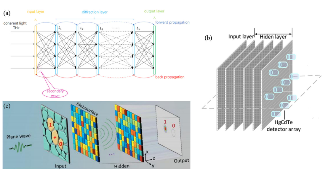
Photonics is one of the newest sciences. Photonics is the study of light and interaction with other particles or materials. May be could say photonic science includes and is based on 4 main topics: 1-ray optics, 2-Wave optics, 3-Electromagnetic optics, and 4- Quantum optics quantum optics is the best complete theory about all of physics and the world. This science is like a bridge between Optics or Physics and the other sciences such as Electronic or chemistry and biology and so more. You should be very careful in the definition of photonic and optic. The optic is not photonic and vice versa but the optic is a subpart and one important part of photonic. We in photonics be faced with interaction among waves and collision between particles - specially Photons - with the matter. Also, we concentrate on other applications of it, for example, modulation and modifying waves. Photonics has explained many topics such as Fiber, Imaging, Laser Processing, Tera Hertz, etc. At figure 4 one of the application of photonic was shown.
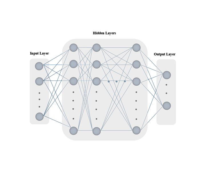
Neural networks is a modern method of knowledge that is very applicable because it is very active in treatment ways and computing systems. Or in a more accurate definition we could say, is a series of algorithms that endeavors to recognize underlying relationships in a set of data through a process that mimics the way the human brain operates. Neural networks help us to be a classifier. Neural networks can adapt to changing input; so the network can generate the best possible result without needing to redesign the output criteria. It is related to Neurons and it has very important rules and interaction with other sciences. By it, we can transform our information and process them very quickly.
For simple showing been entered some inputs and had been done many multiplications of math on them and finally, we received outputs.
Consequently, now photonic science
is a perfect alternative for electronic [ 28,29 ].
At first, much manufacturing was bulky and made from insufficient technology and Neural Network concepts. Recently
have changed, first of all, because RC enabled the reduction of analog electronic and photonic RNN.
[ 30-34 ].
In addition, integrated photonic platforms also have been completed and today they are practical [ 35 ].
Yet, Neural Networks
consist of numerous photonic nonlinear nodes. So it has been demonstrated
only in delay systems [ 36 ].
Due to the time multiplexing, delay system Neural Networks require such a subsidiary foundation [6].
Photonic technologies also are widely applied and have validity in our daily life.
Integrated photonics ar first [40], and after that indium phosphide–based technologies [41], emerged for optical communication, metro, and also for short-range links. The advantages of optics that are very important: 1- larger bandwidth-distance crops,
2- the massive parallelism, 3- low propagation loss, etc. This can be transmitted through optical fibers [42,9].
In this research, we want to answer important questions. The first question is:Can we progress and optimize Q-factor at 3L cavity?. The second question that can ask is Although Electronic has progressed at many parts of industrial work or other things, what is the location of Photonics and what are the challenges between Electronics and Photonics?
Research Methodology
In this review article, we explored many articles from strong scientists and experts around the world. We tried to apply the main topics and research among many of the articles that we used. These articles some of them were very bold and perfect. This sentence means some articles such as the survey article have been applied many times in this exploration and they were very useful. Well actually as you saw most of these articles were published generally from 2017 to 2022. After this introduction, we explain an overview of a photonic neural network at Application part. Then we extend some fundamental concepts and finally, we will discuss the advantages and disadvantages.
2 Fundamental Concepts
2.1 Roadmap on material-function mapping
some parts of this topic explained the differences between photonic and memristor. (pros and cons). At it, we can see the perception model, which is the first neural network. inputs and outputs and also summation and finally activation function are shown in figure 5 part b.
Strength and pain points for photonic information processing:
First, we are going to say some benefits: 1- Real-time. 2- Parallelism, etc.
And now we will say the disadvantages: 1- Efficient memory. 2- Functionality.
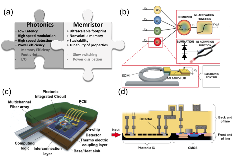
2.2 Integrated Photonics
This subject provides a good manner to discover huge-scale optical networks on chips. one of the applications of photonics is less distortion. Also, the modern technology of it, standardization of silicon photonic integrated circuits (PIC) has led to the proliferation of shorter-distance photonic links.
We have some implementation:
For photonic:
| (1) |
In the above equation , and are cartesian components and is time. Photonic devices have become very dense compared to now.
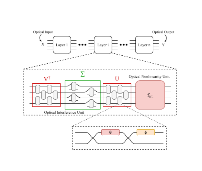
2.3 Neuromorphic Photonics
It is useful to work by matrix-vector multiplication (MVM).
Now again we want to talk about some information related to silicon. Silicon photonic modulator neuron is one of the topics at neuromorphic. This field exists in pivotal and unexplored regimes of machine intelligence. We have to say neuromorphic photonic systems can calculate and operate about 8 orders faster than electronic samples.
Then we are going to define a device: The modulator neuron is an optical-to-electrical-to-optical device consisting of two balanced photodetectors. (PDs)
Characterization: There are three independent quantities:
1- Heater current bias ()
2- Modulator current bias ()
3- Optical power into the and parts.( , ,…)
In this device, we process responses to high-bandwidth inputs and responses to multiple inputs and responses to pulses and capability. So we designed a silicon photonic circuit based on two photodetectors.
| (2) |
| (3) |
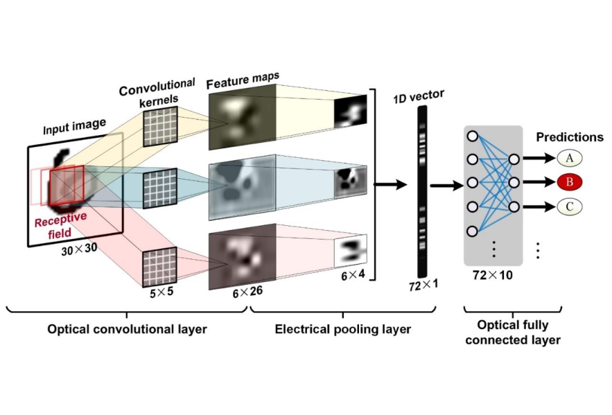
2.4 Convolutional Neural Network (CNN)
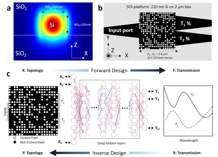
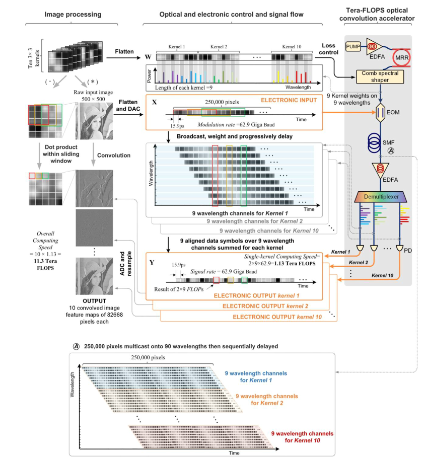
Convolutional Neural Network (CNN) is one the important part of AI systems. This is a powerful series of artificial neural networks. The application of CNN is at the recognition of handwritten digit images perfectly and strongly. We need the shaped microvomb’s optical spectrum and the corresponding kernel weights. Figure 9 showed this proccesing[11].
Convolutional Neural Network is a great kind of deep learning. In 1959, Hubel and Wiesel found that cells in the animal
visual cortex are responsible for detecting light in receptive fields. And then Kunihiko
Fukushima could propose the recognition in 1980, which could be regarded as the predecessor of CNN. In
1990, LeCun could publish a seminal paper establishing the modern framework of CNN, and later
improved it [20].
2.5 Optical Neural Networks (ONNs)
Optical neural networks can process information in free space and an integrated platform. Over many years, the system of integrated circuits has been restricted by Moore’s law [21]. Today, Optical Neural Networks (ONNs) in photonic devices are higher efficiency and have lower power consumption than electronic platforms ANN in deep learning consists of research attention such as image processing, self-driving vehicles, games, and robots[2]!
Photonic devices also incorporate those
nonvolatile PCMs thus can:
1- realize optical memories, 2- perform
in-memory computing simply[64–66].
increasing for these phase-change photonic devices in a scalable
network has been
designed and developed[66–69,15].
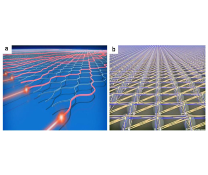
2.6 Three-dimentional waveguide interconnects
We had some problems or limitations with two dimension work. For example, limitation in size by lithography due to disadvantages of scaling. Using one good manner to overcome many bottlenecks in NN communication is to discover integrated circuits holding to a NN’s difficult topology.
3D interconnects of the photonic waveguide are very useful in 3D commercial use direct-laser writing system called (Photonic Professional GT). Also, commercial NN uses heavily employed by Google features.
We realized large-scale 3D photonic interconnects. Waveguides are a diameter
of 1.2 m that could create two-photon polymerization. By use of this strategy,
we discovered routing topologies at 3 dimensions. These
methods were oriented mostly toward applications in Neural Networks [19].
2.7 Large-scale Optical Neural Networks
One of the important features and instruments that name is . It is useful for the implementation of a single layer. In this location, we do many acts of math, for example, multiplier integrator.
| (4) |
| (5) |
In this equation, are matrix dimensions.
We use this method to compute the required matrix products optoelectronically without the need for an all-optical nonlinearity. Computing used by Monte Carlo simulations.
Also, this feature is a new kind of photonic accelerator that is scalable to values of that are larger than networks. And also can be operated at high (Gigahertz) velocities and consume very low energies. For coherent matrix we will have relationship between and layers[14]:
| (6) |
3 Applications of Photonic neural networks
PHOTONICS has been realized for its important role in communication systems. For example, fiber optic links form the world’s telecommunications. So we could say a photonic
waveguide, with sizes ranging about (80 m)
, can carry information very easily per second without depending on distance [17].
Today machine learning science is developed for many tasks and it uses in
a large number of processing and many other applications such as easy calculation, image information
classification, speech recognition, language translation, decision making, web searches,
etc. Artificial Neural Networks or ANN also are useful for
processing data series, combining and analyzing information quickly [5].
Electronic pieces of information are very necessary but electronics face a main impasse: data transfer between processors and memories is constrained by unavoidable bandwidth limitations.
One another application of photonic is at the L3 cavity:
Our purpose is to find ways to optimize and increase the Q-factor in 3L. The cost of this work is very much so we have to use NN or Neural Network. This work is done in several steps:
1. Preparing phase, 2. Learning phase, 3. Structure search phase and, finally 4. Validation and update phases[8].
Another important use of photonics well actually as you saw, is Deep Neural networks:
They are used in a range of applications such as image and video processing, diagnostic medical imaging, speech recognition, and conversational AI.
Deep learning ways had been tried to obtain non-linear operators
that transform the representation from the previous levels into a higher one.
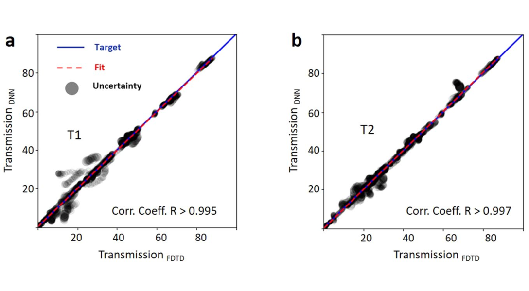
We face an important concept called optical response. The optical response was predictable. By using deep learning neural networks could predict the optical response of such information.
Also, we used Bernoulli probably classifier. (for hole location) and we used the Gaussian log-likelihood loss function[18]:
| (7) |
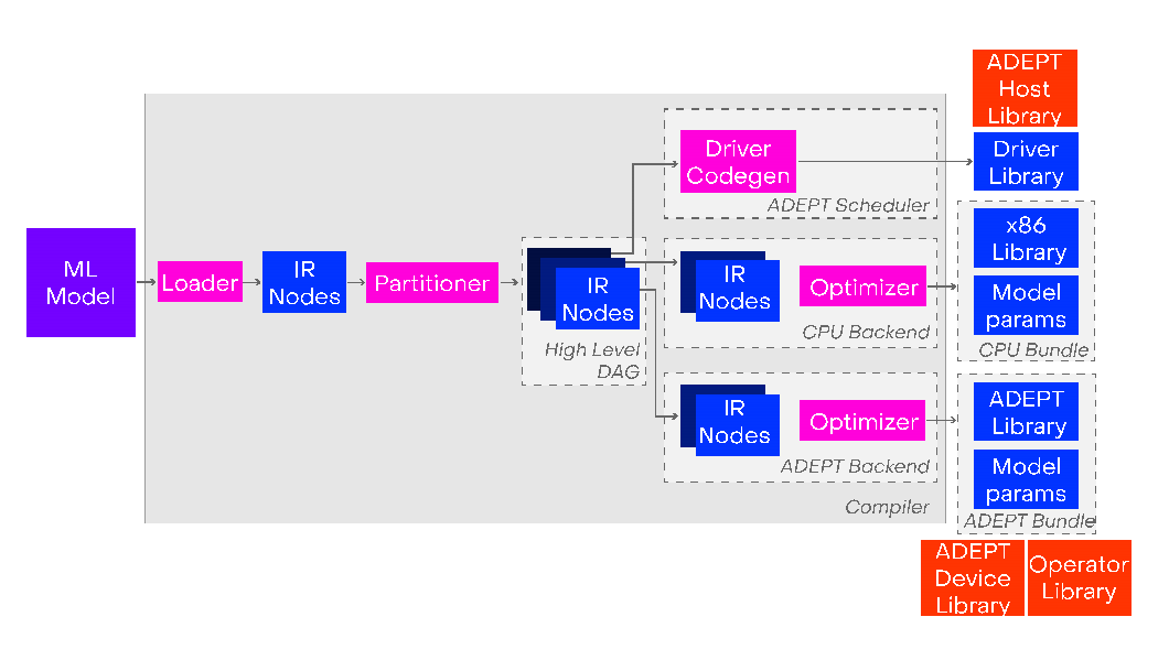
Also, we explain the process of executing a given DNN on ADEPT. The compiler (Figure 6) takes a DNN model as input and compiles it to generate a program specified via a graph on tensor types. It has a cost-model-based partitioner that creates a directed acyclic graph (DAG) with 3 sets of nodes: operations to execute on the host CPU (e.g., input pre- and post-processing, etc.); operations to execute on ADEPT (e.g., ML operations such as GEMM, convolutions, non-linear operations, etc.); and a set of driver nodes for moving data between the host and ADEPT[3]. Emerging photonic neural networks increased computing speed by 2-3 orders of magnitude. Two advanced features were: weighted sum and NL activation, Absence of NL(non-linear) in optical systems have severely limited its usefulness in deep learning computing. All works and activities goal to progress both speed and energy efficiency. One of these achievements is ANN or Artificial Neural Networks. Then we have to discuss biology. Biological neural networks consist of a huge number of neurons. In this work, the optimization variables for all ONN are controlled by a kind of perfect velocity [12]:
| (8) |
That is the equation:
Are acceleration constants.
For designing integrated photonic devices have to say
integrated photonics manners had became powerful tools for processing at classical and
quantum information. Integrated photonics is used for
1- optical interconnects[ 43 ], 2- signaling [ 44 ], and finally photonic processing [ 45 ].About Processing
quantum information have to say it also indicates great agreement [ 46, 47 ], with discovered
advantages at quantum communications [ 48 ] Also
for quantum simulation [ 49, 50 ].
Designing integrated photonics circuits, however, remains a major impasse
[ 51 ]. But current designs are complicated by computational capability [52,10].
Photonic physic science exhibits properties distinct from those
of electronics in terms of multiplexing, energy dissipation,
and cross-talk. These properties are favorable for dense,
high-bandwidth interconnects [53] in addition to configurable analog signal processing [54–56]. As result,
neuromorphic photonic systems also could operate in 6–8 orders-
of magnitude faster than neuromorphic electronics [63]
with the possibility of higher energy effects than others [57]. Optical neural binds based on field progress in 1- free space [58, 59],2- holograms [60, 61], and also fiber [62] have
been shown but were not widely corresponded, in part because they are could not be integrated on a chip[13,16].
We used a table for summarizing of main studied information. The information brought at the bottom:
| References | Publication year | Main idea |
|---|---|---|
| Mario et al.[4] | 2019 | providing a new manner to pave the way for emerging photonic-electronic neural networks devices by finding a detailed knowledge in the single nodes |
| Mohammad et al.[18] | 2019 | using a deep neural network to introduce a method for predicting optical response |
| LORENZO et al.[5] | 2019 | reviewing for achievement at photonic neural network |
| TIAN et al.[12] | 2019 | proposing a strategy for learning neural networks based on the neuron to design and train ONN |
| ALEC et al.[10] | 2019 | training ANNs to model both strip waveguides and chirped Bragg gratings using a small number of simple input and output parameters relevant to designers of integrated photonic circuits |
| Xingyuan et al.[11] | 2020 | Optical neural networks ways based on high speed and low energy consumption |
| Cansu et al.[3] | 2021 | introducing a complete electronic- a photonic system that combines an electronic host processor and DRAM alongside an electronic-photonic accelerator (called ADEPT) |
4 Discussion
This presented research is tried to show this note that photonics and neural networks and finally the combination of these two are important so much for continuing progress in doing and processing information. with photonics and other applications of photonics is still open. It has been seen that the advantages of photonic and photonic neural networks were very useful and the role of these sciences in the world is very important. This research has used and has studied about 80 articles but about 18 articles were main for our research. We understood that these applications are not the end of the photonic neural network’s way. In addition, the photonic manufacturing of the nonlinear function and concepts of vector-matrix are very big relevant aspects. This paper also has presented the advantages and disadvantages of neural networks and compared them to electronic devices and methods. Well actually as you saw in this research we tried to show L3 cavity can optimize by designing a neural network and we can increase the Q-factor in the L3 cavity. After this topic, we have to accept that photonics increases the speed of processing and even calculation because it is combined with neural networks, especially at short wavelengths and electronics are not able to achieve them. In many of these articles, these sentences said [11,12] although we knew electronic science is very valid in all of part of industrial and other parts of the world. One another aspect of this article was this question Where are we now? or What are the applications of photonic neural networks? In this research almost we could show What is the photonics? or What is the neural networks?. And then we explained What is the relation between photonics and neural networks?. In addition, we use some other articles that studied each of the topics separately. For example for CNN and ONN, we used related articles of them. Finally, we should say we also used and got help from many other related articles except 17 main articles. All of the other articles are referenced in the final part.
5 References
[1] Zhigang Chen, and Mordechai Segev.
Highlighting photonics: looking
into the next decade. (2021)
[2]
Jia Liu1, Qiuhao Wu1, Xiubao Sui1, Qian Chen1, Guohua Gu1, Liping Wang1 and Shengcai Li2. Research progress in optical neural
networks: theory, applications, and
developments. (2021)
[3] Cansu Demirkiran Furkan Eris Gongyu Wang Jonathan Elmhurst Nick Moore
Nicholas C. Harris Ayon Basumallik Vijay Janapa Reddi Ajay Joshi Darius Bunandar
Boston University Lightmatter Harvard University. An Electro-Photonic System
for Accelerating Deep Neural Networks.(2021)
[4] Cite as: APL Mater. 7, 100903 (2019); https://doi.org/10.1063/1.5109689
Submitted: 10 May 2019 • Accepted: 19 September 2019 • Published Online: 10 October 2019
Mario Miscuglio, Gina C. Adam, Duygu Kuzum, et al. Roadmap on material-function mapping for
photonic-electronic hybrid neural networks.(2019)
[5] LORENZO DE MARINIS , MARCO COCOCCIONI , (Senior Member, IEEE),
PIERO CASTOLDI , (Senior Member, IEEE),
AND NICOLA ANDRIOLLI , (Senior Member, IEEE). Photonic Neural Networks: A Survey. (2019)
[6]
J. BUENO , S. MAKTOOBI , L. FROEHLY , I. FISCHER , M. JACQUOT , L. LARGER , AND D. BRUNNER2
1Instituto de F´sica ı Interdisciplinar y Sistemas Complejos, IFISC (UIB-CSIC), Campus Universitat de les Illes Baleares, E-07122 Palma de Mallorca, Spain
2FEMTO-ST Institute/Optics Department, CNRS and University Bourgogne Franche-Comté, 15B avenue des Montboucons,
25030 Besançon Cedex, France.
Reinforcement learning on a large-scale
photonic recurrent neural network.(2018)
[7]
MARIO MISCUGLIO , ARMIN MEHRABIAN , ZIBO HU , SHAIMAA I. AZZAM ,
JONATHAN GEORGE, ALEXANDER V. KILDISHEV, MATTHEW PELTON,
AND VOLKER J. SORGER.
All-optical nonlinear activation function for
photonic neural networks [Invited]. (2018)
[8] Takashi Asano and Susumu Noda. Iterative optimization of photonic crystal
nanocavity designs by using deep neural networks.(2019)
[9] Pascal Stark, Folkert Horst, Roger Dangel, Jonas Weiss and Bert Jan Offrein. Opportunities for integrated photonic neural
networks.(2020)
[10] ALEC M. HAMMOND AND RYAN M. CAMACHO.
Designing integrated photonic devices using
artificial neural networks.(2019)
[11] Xingyuan Xu, Mengxi Tan, Bill Corcoran, Jiayang Wu, Andreas Boes, Thach G. Nguyen,
Sai T. Chu, Brent E. Little, Damien G. Hicks, Roberto Morandotti, Arnan Mitchell, and
David J. Moss.
11.0 Tera-FLOP/second photonic convolutional accelerator
for deep learning optical neural networks.
[12] TIAN ZHANG, JIA WANG, YIHANG DAN, YUXIANG LANQIU,
JIAN DAI , XU HAN , XIAOJUAN SUN , AND KUN XU. Efficient training and design of photonic neural
network through neuroevolution.(2019)
[13] Alexander N. Tait, Thomas Ferreira de Lima, Mitchell A. Nahmias,
Heidi B. Miller,y Hsuan-Tung Peng, Bhavin J. Shastri,y and Paul R. Prucnal
Department of Electrical Engineering, Princeton University, Princeton, NJ 08544, USA
(Dated: January 1, 2019). A silicon photonic modulator neuron.(2018)
[14]
Ryan Hamerly, Liane Bernstein, Alexander Sludds, Marin Soljačić , and Dirk Englund
Research Laboratory of Electronics, MIT, 50 Vassar Street, Cambridge, Massachusetts 02139, USA.
Large-Scale Optical Neural Networks Based on Photoelectric Multiplication. (2019)
[15] Changming Wu, Heshan Yu, Seokhyeong Lee1, Ruoming Peng, Ichiro Takeuchi, and MoLi.
Programmable phase-change metasurfaces on
waveguides for multimode photonic convolutional
neural network.(2021)
[16]
TYLER W. HUGHES, MOMCHIL MINKOV, YU SHI, AND SHANHUI FAN
Department of Applied Physics, Stanford University, Stanford, California 94305, USA
Ginzton Laboratory and Department of Electrical Engineering, Stanford University, Stanford, California 94305, USA
Corresponding author: shanhui@stanford.edu Training of photonic neural networks through
in situ backpropagation and gradient measurement.(2018)
[17] Mitchell A. Nahmias , Thomas Ferreira de Lima , Alexander N. Tait , Hsuan-Tung Peng ,
Bhavin J. Shastri, Member, IEEE, and Paul R. Prucnal, Fellow, IEEE Photonic Multiply-Accumulate Operations for
Neural Networks.(2020)
[18] Inverse Mohammad H. tahersima , Keisuke Kojima , toshiaki Koike-Akino, Devesh Jha ,
Bingnan Wang, Chungwei Lin, and Kieran parsons
Design of Integrated photonic
power splitters. Deep Neural Network (2019)
[19]
Johnny Moughames, Xavier Porte, Michael Thiel, Gwenn Ulliac,
AND
Laurent Larger, Maxime Jacquot, Muamer Kadic, Daniel Brunner. Three-dimensional waveguide interconnects for
scalable integration of photonic neural networks. (2020)
[20] Recent Advances in Convolutional Neural Networks.
Jiuxiang Gua, Zhenhua Wangb, Jason Kuenb, Lianyang Mab, Amir Shahroudyb, Bing Shuaib, Ting
Liub, Xingxing Wangb, Gang Wangb, Jianfei Caic, Tsuhan Chenc (2017)
[21] A Survey of Convolutional Neural Networks:
Analysis, Applications, and Prospects.
Zewen Li, Fan Liu, Member, IEEE, Wenjie Yang, Shouheng Peng, and Jun Zhou, Senior Member, IEEE. (2021)
[22] Zavareh, PH.; Safayari, A.; Bolhasani, H. BCNet: A Deep Convolutional Neural Network for Breast Cancer Grading. arXiv:2107.05037, Jul 2021.
[23]
Y. Lu, M. Stegmaier, P. Nukala, M. A. Giambra, S. Ferrari, A. Busacca,
W. H. P. Pernice, and R. Agarwal, Nano Lett. 17, 150 (2017).
[24]
C. Ríos, M. Stegmaier, P. Hosseini, D. Wang, T. Scherer, C. D. Wright,
H. Bhaskaran, and W. H. P. Pernice, Nat. Photonics 9, 725 (2015).
[25]
C. Ríos, N. Youngblood, Z. Cheng, M. L. Gallo, W. H. P. Pernice, C. D. Wright,
A. Sebastian, and H. Bhaskaran, Sci. Adv. 5 , eaau5759 (2019).
[26]
J. Zheng, A. Khanolkar, P. Xu, S. Colburn, S. Deshmukh, J. Myers, J. Frantz,
E. Pop, J. Hendrickson, J. Doylend, N. Boechler, and A. Majumdar, Opt. Mater.
Express 8 , 1551 (2018).
[27]
J. Feldmann, N. Youngblood, C. D. Wright, H. Bhaskaran, and W. H. P. Pernice,
Nature 569, 208 (2019)
[28] K. Wagner and D. Psaltis, “Multilayer optical learning networks, ” Appl.
Opt. 26, 5061–5076 (1987).
[29] C. Denz, Optical Neural Networks (Springer Vieweg, 1998).
[30] L. Appeltant, M. C. Soriano, G. Van der Sande, J. Danckaert, S. Massar,
J. Dambre, B. Schrauwen, C. R. Mirasso, and I. Fischer, “Information
processing using a single dynamical node as a complex system, ” Nat.
Commun. , 468 (2011).
[31]
F. Duport, B. Schneider, A. Smerieri, M. Haelterman, and S. Massar,
“All-optical reservoir computing, ” Opt. Express 20, 22783–22795 (2012).
[32]
Y. Paquot, F. Duport, A. Smerieri, J. Dambre, B. Schrauwen, M.
Haelterman, and S. Massar, “Optoelectronic reservoir computing, ” Sci.
Rep. 2, 287 (2012).
[33]
L. Larger, M. C. Soriano, D. Brunner, L. Appeltant, J. M. Gutierrez, L.
Pesquera, C. R. Mirasso, and I. Fischer, “Photonic information process-
ing beyond Turing: an optoelectronic implementation of reservoir
computing, ” Opt. Express 20, 3241–3249 (2012).
[34]
D. Brunner, M. C. Soriano, C. R. Mirasso, and I. Fischer, “Parallel pho-
tonic information processing at gigabyte-per-second data rates using
transient states, ” Nat. Commun. , 1364 (2013).
[35]
Y. Shen, N. C. Harris, S. Skirlo, M. Prabhu, T. Baehr-Jones, M.
Hochberg, X. Sun, S. Zhao, H. Larochelle, D. Englund, and M. Soljacic,
“Deep learning with coherent nanophotonic circuits, ” Nat. Photonics 11,
441–446 (2017).
[36]
P. Antonik, M. Haelterman, and S. Massar, “Online training for high-
performance analog readout layers in photonic reservoir computers, ”
Cognit. Comput. , 297–306 (2017).
[37]
B. J. Shastri, A. N. Tait, T. F. de Lima, M. A. Nahmias, H.-T. Peng, and P. R. Prucnal, “Principles of
Neuromorphic Photonics,” arXiv:1801.00016 [physics] 1–37 (2018).
[38]
A. N. Tait, T. F. de Lima, E. Zhou, A. X. Wu, M. A. Nahmias, B. J. Shastri, and P. R. Prucnal, “Neuromorphic
photonic networks using silicon photonic weight banks,” Sci. Rep. 7 (1), 7430 (2017).
[39]
M. A. Nahmias, B. J. Shastri, A. N. Tait, T. F. de Lima, and P. R. Prucnal, “Neuromorphic Photonics,” Optics
and amp; Photonics News, OPN 29 (1), 34–41 (2018).
[40] A. E.-J. Lim, J. Song, Q. Fang, et al., “Review of silicon photonics
foundry efforts, ” IEEE J. Sel. Top. Quantum Electron. , vol.20,
no. 4, pp. 405–416, Jul. 2014.
[41] H. Zhao, S. Pinna, F. Sang, et al., “High-power indium phosphide
photonic integrated circuits, ” IEEE J. Sel. Top. Quantum Electron. ,
vol. 25, no. 6, pp. 1–10, Nov. 2019.
[42] M. A. Taubenblatt, “Optical interconnects for high-performance
computing, ” J. Light. Technol. , vol. 30, no. 4, pp. 448–457, Feb.
2012.
[43]
M. J. Heck, H.-W. Chen, A. W. Fang, B. R. Koch, D. Liang, H. Park, M. N. Sysak, and J. E. Bowers, “Hybrid silicon
photonics for optical interconnects,” IEEE J. Sel. Top. Quantum Electron. 17 (2), 333–346 (2011).
[44]
T. Barwicz, H. Byun, F. Gan, C. W. Holzwarth, M. A. Popovic, P. T. Rakich, M. R. Watts, E. P. Ippen, F. X. Kärtner,
H. I. Smith, J. S. Orcutt, R. J. Ram, V. Stojanovic, O. O. Olubuyide, J. L. Hoyt, S. Spector, M. Geis, M. Grein, T.
Lyszczarz, and J. U. Yoon, “Silicon photonics for compact, energy-efficient interconnects (invited),” J. Opt. Netw.
6 (1), 63–73 (2007).
[45]
J. Wang, “Chip-scale optical interconnects and optical data processing using silicon photonic devices,” Photon. Netw.
Commun. 31 (2), 353–372 (2016).
[46]
A. Orieux and E. Diamanti, “Recent advances on integrated quantum communications,” J. Opt. 18 (8), 083002 (2016).
[47]
F. Flamini, N. Spagnolo, and F. Sciarrino, “Photonic quantum information processing: a review,” Rep. Prog. Phys.
82 (1), 016001 (2019).
[48]
D. Bunandar, A. Lentine, C. Lee, H. Cai, C. M. Long, N. Boynton, N. Martinez, C. DeRose, C. Chen, M. Grein, D.
Trotter, A. Starbuck, A. Pomerene, S. Hamilton, F. N. C. Wong, R. Camacho, P. Davids, J. Urayama, and D. Englund,
“Metropolitan quantum key distribution with silicon photonics,” Phys. Rev. X 8 (2), 021009 (2018).
[49]
N. C. Harris, G. R. Steinbrecher, M. Prabhu, Y. Lahini, J. Mower, D. Bunandar, C. Chen, F. N. C. Wong, T. Baehr-Jones,
M. Hochberg, S. Lloyd, and D. Englund, “Quantum transport simulations in a programmable nanophotonic processor;
EP,” Nat. Photonics 11 (7), 447–452 (2017).
[50]
X. Qiang, X. Zhou, J. Wang, C. M. Wilkes, T. Loke, S. O’Gara, L. Kling, G. D. Marshall, R. Santagati, T. C.
Ralph, J. B. Wang, J. L. O’Brien, M. G. Thompson, and J. C. F. Matthews, “Large-scale silicon quantum photonics
implementing arbitrary two-qubit processing,” Nat. Photonics 12 (9), 534–539 (2018).
[51]
L. Chrostowski and M. Hochberg, Silicon Photonics Design: From Devices to Systems (Cambridge University, 2015).
[52]
W. Bogaerts and L. Chrostowski, “Silicon Photonics Circuit Design: Methods, Tools and Challenges,” Laser
Photonics Rev. 12 (4), 1700237 (2018).
[53]
S. Rakheja and V. Kumar, in Quality Electronic De-
sign (ISQED), 2012 13th International Symposium on
(2012) pp. 732–739.
[54] A. M. Weiner, Optics Communications 284, 3669
(2011), Special Issue on Optical Pulse Shaping, Arbi-
tray Waveform Generation, and Pulse Characterize-
tion.
[55] D. P´erez, I. Gasulla, L. Crudgington, D. J. Thomson,
A. Z. Khokhar, K. Li, W. Cao, G. Z. Mashanovich, and
J. Capmany, Nature Communications 8, 636 (2017).
[56] W. Liu, M. Li, R. S. Guzzon, E. J. Norberg, J. S. Parker,
M. Lu, L. A. Coldren, and J. Yao, Nat. Photon. 10 , 190
(2016).
[57] T. Ferreira de Lima, B. J. Shastri, A. N. Tait, M. A.
Nahmias, and P. R. Prucnal, Nanophotonics 6 (2017),
10.1515/nanoph-2016-0139.
[58] D. Brunner and I. Fischer, Optics letters 40, 3854
(2015).
[59] D. Psaltis and Y. Quio, Opt. Photon. News 1, 17 (1990).
[60] J. W. Goodman, A. R. Dias, and L. M. Woody Opt.
Lett. 2, 1 (1978).
[61] P. Asthana, G. P. Nordin, J. Armand R. Tanguay, and
B. K. Jenkins, Appl. Opt. 32, 1441 (1993).
[62] M. Hill, E. E. E. Frietman, H. de Waardt, G.-D. Khoe,
and H. Dorren, IEEE Trans. Neural Networks 13 , 1504
(2002).
[63] B. J. Shastri, A. N. Tait, T. F. de Lima, M. A. Nah-
mias, H.-T. Peng, and P. R. Prucnal, arXiv:1801.00016
(2018).
[64] Bocker, R. P. Matrix multiplication using incoherent optical techniques. Appl.
Opt. 13, 1670–1676 (1974).
[65] Ríos, C. et al. In-memory computing on a photonic platform. Sci. Adv. 5 ,
eaau5759 (2019).
[66] Chakraborty, I., Saha, G. and Roy, K. Photonic in-memory computing primitive
for spiking neural networks using phase-change materials. Phys. Rev. Appl. 11,
014063 (2019).
[67] Caulfield, H. J., Kinser, J. and Rogers, S. K. Optical neural networks. Proc. IEEE
77, 1573–1583 (1989).
[68] Feldmann, J. et al. Parallel convolution processing using an integrated
photonic tensor core. arXiv preprint arXiv:2002.00281 (2020).
[69] Feldmann, J., Youngblood, N., Wright, C. D., Bhaskaran, H. and Pernice, W. H.
P. All-optical spiking neuro synaptic networks with self-learning capabilities.
Nature 569, 208–214 (2019).
6 Authors
|
Mohammad Ahmadi
BSc. Physics, University of Isfahan, 2017-2021. MSc. Photonics, Institute of Laser and Plasma, Shahid Beheshti University, Tehran, Iran, 2021-now. Fields of Interest: Optical Fiber Sensors, Quantum Optics, Optical Designing, Quantum Information, Laser Biophotonic, Machine Learning |
![[Uncaptioned image]](/html/2302.08390/assets/2.jpg)
|
|
Hamidreza Bolhasani
Ph.D. / Researcher / Visiting Professor BSc. Physics, University of Isfahan, 2004-2008. MSc. Information Technology, Science and Research Branch, Islamic Azad University, Tehran, Iran, 2015-2018. Ph.D. Computer Engineering, Science and Research Branch, Islamic Azad University, Tehran, Iran, 2018-2023. Fields of Interest: Artificial Intelligence, Machine Learning, Deep Learning, Deep Learning Accelerators, Computer Architecture, Neural Networks |
![[Uncaptioned image]](/html/2302.08390/assets/1.jpg)
|