Perspective: strain and strain gradient engineering in membranes of quantum materials
Abstract
Strain is powerful for discovery and manipulation of new phases of matter; however, the elastic strains accessible to epitaxial films and bulk crystals are typically limited to small (), uniform, and often discrete values. This Perspective highlights new directions for strain and strain gradient engineering in free-standing single crystalline membranes of quantum materials. Membranes enable large (), continuously tunable strains and strain gradients via bending and rippling. Moreover, strain gradients break inversion symmetry to activate polar distortions, ferroelectricity, chiral spin textures, novel superconductivity, and topological states. Recent advances in membrane synthesis by remote epitaxy and sacrificial etch layers enable extreme strains in new materials, including transition metal oxides and Heusler compounds, compared to natively van der Waals (vdW) materials like graphene. We highlight new opportunities and challenges for strain and strain gradient engineering in membranes of non-vdW materials.
I Introduction
The properties of quantum materials with highly localized and orbitals can be highly sensitive to changes in bond lengths, bond angles, local coordination, and symmetry. Strain is a powerful knob for tuning these parameters, with striking examples including strain-induced superconductivity in epitaxial RuO2 films Ruf et al. (2021), strain-induced ferroelecticity in SrTiO3 Schlom et al. (2007), and strain-induced changes in magnetic ordering in magnetic shape memory alloys Song et al. (2020). However, the strains accessible to bulk materials and epitaxial films are typically limited to before relaxation via dislocations Matthews and Blakeslee (1974); People and Bean (1985); Van Der Merwe (1963). Moreover, in epitaxial films the strain is static and discrete, based on the lattice mismatch between particular film and substrate combinations. As a result, many quantum properties remain out of reach.
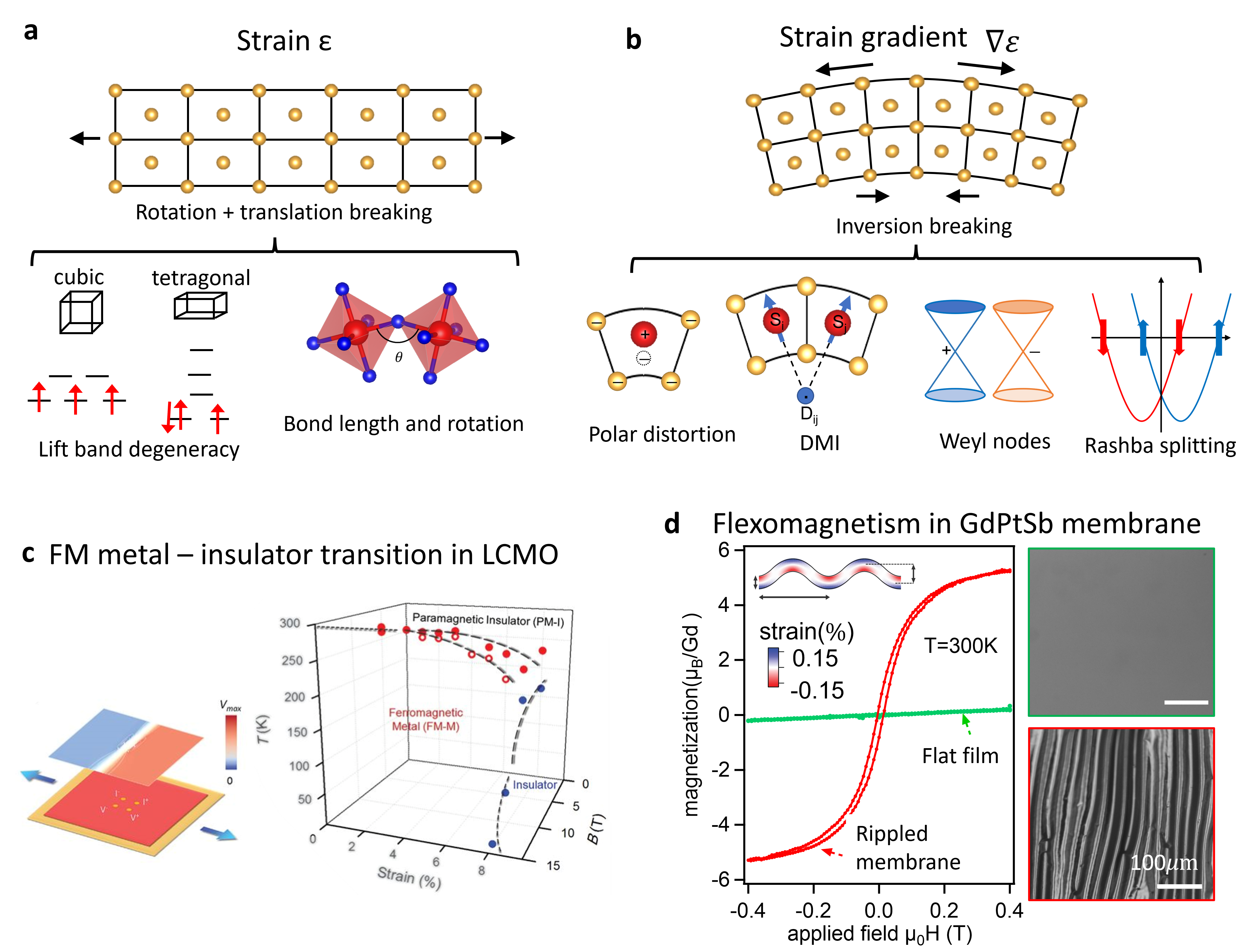
This Perspective highlights new opportunities for strain and strain gradient engineering in single crystalline membranes of quantum materials, beyond natively vdW materials. Free-standing membranes enable two regimes that are inaccessible in films and bulk crystals (Fig. 1). First, membranes and other free-standing nanostructures can sustain much larger elastic strains (8% in (La,Ca)MnO3 membranes Hong et al. (2020) and 10% in BaTiO3 Dong et al. (2019)), compared to the limit for films and bulk crystals. Second, membranes enable controlled strain gradients via bending and rippling Du et al. (2021). Whereas uniform strain breaks rotational and translational symmetries (Fig. 1a), strain gradients break inversion symmetry. Inversion breaking is the necessary ingredient for ferroelectric polar distortions, nonlinear optical responses, Dzyaloshinskii-Moriya interaction (DMI)-induced chiral spin textures, and Rashba splitting (Fig. 1b).
Recent advances in remote epitaxy Kim et al. (2017); Kum et al. (2020); Du et al. (2021, 2022); Yoon et al. (2022) and etch release layers Hong et al. (2020); Dai et al. (2022) enable the synthesis of ultrathin membranes of quantum materials, including Heusler compounds and transition metal oxides. These synthesis advancements enable extreme strain to be applied to new classes of ultrathin membranes, which until recently were mainly limited to easily exfoliatable van der Waals (vdW) materials like graphene and transition metal dichalcogenides Si et al. (2016); Peng et al. (2020a). We highlight opportunities for discovery of new properties via large strains and strain gradients in these materials (Section II). Realization of these properties relies on new approaches for single crystalline membrane synthesis, understanding and controlling their extreme mechanical properties, and feedback from computational modelling (Section III). We conclude with an outlook on static and nonequilibrium stains (Section IV).
II Opportunities
II.1 Magnetism, flexomagnetism, and skyrmions
Homogeneous strains couple strongly to magnetism via piezomagnetism () and magnetostriction (). Microscopically, strain tunes magnetic exchange via the bond lengths and bond angles, and tunes the band degeneracies and occupancies via change in symmetry Zhang et al. (2018a). Many Heusler compounds and transition metal oxides have rich magnetic properties Casper et al. (2012); Bibes and Barthelemy (2007); Bibes et al. (2011). Larger strain in membranes have the potential to tune magnetic properties more substantially. As an example, strains in (La,Ca)MnO3 membranes induce a ferromagnetic metal metal to insulator transition Hong et al. (2020) (Fig. 1c).
Magnetism can also couple strongly to strain gradients, which is termed flexomagnetism () Eliseev et al. (2011); Lukashev and Sabirianov (2010); Eliseev et al. (2009). Whereas strain gradients are difficult to control in bulk crystals and epitaxially clamped films, we recently demonstrated an antiferromagnetic to ferro/ferrimagnetic transition upon rippling in GdPtSb membranes, in the first experimental example of flexomagnetism Du et al. (2021) (Fig. 1d). Although the microscopic mechanism is not well understood, we speculate that strain gradients enhance the DMI, leading to canted ferrimagnetism in the rippled GdPtSb membranes. Microscopic measurements and theory are required to understand the flexomagnetic response.
Inversion-breaking strain gradients can also tune or induce chiral spin textures such as skyrmions, via tuning the DMI. As proof of concept, recent experiments on partially relaxed (La,Sr)MnO3 (LSMO) films show signatures of skyrmions, induced by inversion-breaking strain gradients along the growth direction Zhang et al. (2021). We anticipate even greater control of skyrmions in bent LSMO membranes, which allow the strain gradient to be tuned more precisely and continuously rather spontatneous strain relaxation in LSMO films.
Theory predicts skyrmions in other bent systems. Mesoscale calculations predict highly tunable skyrmions in bent membranes heterostructures of simple metals and a flexo-Hall effect induced by bending Liu et al. (2022). More complex cyclical states are predicted for curved nanotubes of CrI3, due to periodic boundary conditions along the circumference of the nanotube Edström et al. (2022). Strain gradients are also predicted to control skyrmion motion Yanes et al. (2019); Liu et al. (2019); Gorshkov et al. (2022), which could be controlled dynamically on a flexible membrane platform. We anticipate these concepts to apply broadly to membranes of new vdW materials, e.g. rare earth Heusler compounds, magnetic oxides, and chiral intermetallics.
II.2 Ferroelectricity, flexoelectricity, and polar metals
Ferroelectricity requires crystals with broken inversion symmetry that have a unique polar axis. Although homogeneous strain alone does not break inversion, it can tune ferroelecticity in systems that are already ferroelectric or induce ferroelectricity in materials on the verge of being ferroelectric. For example, uniaxial tensile strain induces ferroelectricity in membranes of the quantum paraelectric SrTiO3, by suppressing quantum fluctuations Xu et al. (2020). The absence of strain (clamping) in membranes can also be important: free-standing BaTiO3 membranes display faster switching than epitaxial BaTiO3 films, due to the release from substrate clamping effects Pesquera et al. (2020).
Strain gradients, which break inversion, are even more powerful because they can induce polar distortions in materials that were originally centrosymmetric. The general coupling between ferroelectricity and strain gradients is termed flexoelectricity Kogan (1964); Zubko et al. (2013); Cross (2006); Indenbom et al. (1981). Early experiments quantified the flexoelectric coefficients for few millimeter thick cantilevers of lead magnesium niobate Ma and Cross (2001) and lead zirconate titanate (PZT) Ma and Cross (2005). More recent experiments suggest that 10 nm thick BaTiO3 membranes released from graphene/Ge display an enhanced flexoelectric response compared to bulk Dai et al. (2022). We anticipate broader opportunities for flexoelectricity in ultrathin membranes, where the enhanced elasticity in the ultrathin limit provides access to new regimes for large strains and strain gradients.
Flexoelectric coupling may also enable the switching of polar metals. Unlike ferroelectic insulators, in which the electric polarization can be switched via an applied electric field, in polar metals the electric field is screened out by free carriers. Bending-induced strain gradients provides a means of switching a polar metal without application of an electric field Zabalo and Stengel (2021). First-principles calculations identified LiOsO3 as a promising material for switching via strain gradients Zabalo and Stengel (2021). Other materials, including the high conductivity polar metals LaAuGe and GdAuGeDu et al. (2019, 2022), may also be good candidates.
Finally, ultrathin ferroelectric membranes provide opportunities for mechanically active materials, due to their extreme superelastic responses, large strains, and 180 degree bending. For BiFeO3 membranes, 180 degree bending with 1 micron radius of curvature and reversible elastic strains up to 5.4% are accommodated by a reversible rhombahedral-tetragaonal phase transformations Peng et al. (2020b). For BaTiO3 membranes, large bending strains of 10 percent are reported, which are enabled by continuous dipole rotations of ferroelectric domains Dong et al. (2019). Similar arguments based on phase transformations and domain reorientations may apply for membranes of martensitic materials like shape memory alloys. These materials provide new opportunities for tuning stimuli-responsive materials that undergo large ferroelectric and ferroelastic phase transitions.
II.3 Superconductivity.
Strain and strain gradients in membranes provide opportunities to enhance the critical temperature and critical fields of known superconductors, induce superconductivity in new materials, and tune the pairing symmetry and coupling to other electronic states such as topological states and ferroelectricity.
Strain can enhance the of known superconductors including iron based superconductors and cuprates Engelmann et al. (2013). For example, epitaxial strain enhances the upper critical field of Fe based superconductors Tarantini et al. (2011). In this family of materials, the strength of electronic correlations and are highly dependent on the X-Fe-X bond angle (X = pnictogen or chalcogen), with a maximum Tc when the bond angle is near 109 degrees Okabe et al. (2010); Mandal et al. (2017). This bond angle is typically tuned by alloying, doping, or intercalation Okabe et al. (2010), which introduces disorder. Freestanding membranes provide a path to cleanly and continuously tune the X-Fe-X bond angle via strain and bending-induced strain gradients. Decoupling a monolayer FeSe film from a SrTiO3 substrate also enables the specific effects of interfacial-enhanced superconductivity to be tested Wang et al. (2012); Lee et al. (2014); Tan et al. (2013).
Strained membranes may provide similar opportunities for cuprates and other superconducting oxides. In cuprates, 0.5 % compressive epitaxial strain nearly doubles the of (La,Sr)CuO4 films from 25 K to 49 K Locquet et al. (1998). One challenge for cuprates is that the Tc is also highly sensitive to oxygen stoichiometry Bozovic et al. (2002), making it challenging to compare across separate samples. Membranes provide a possible solution for deconvolving stoichiometry from strain effects by allowing continuous tuning of strain on the same sample. Moreover, membranes enable larger strains and strain gradients.
The large strains and strain gradients in membranes also provide opportunities to induce superconductivity in new materials. Anisotropic strain induces superconductivity in RuO2 films grown on TiO2 (110) Ruf et al. (2021). Membranes provide further tunability for anisotropic strain, since the strain is not limited to particular film-substrate combinations and the strain in different crystallographic directions can be tuned independently. Inversion-breaking strain gradients may also an important new tool: for SrTiO3, ferroelectric polar distortions are thought to stabilize superconductivity Edge et al. (2015), and strain has been shown to tune the Ahadi et al. (2019). Tunable inversion breaking in membranes allows this idea to be tested in other classes of materials, beyond the few existing quantum paraelectrics Müller and Burkard (1979); Rytz et al. (1980).
Finally, inversion breaking strain gradients may find use for tuning the superconducting pairing symmetry Yip (2014). In noncentrosymmeric superconductors, mixtures of spin-singlet and spin-triplet pairing are allowed Gor’kov and Rashba (2001), and interesting topological and magnetoelectric properties are expected Yip (2014). Membranes provide a means to continuously tune the crystalline symmetry of a superconducting material, to distinguish effects strain from disorder.
II.4 Topological states.
Membranes provide an opportunity to tune topological band inversion and band gaps via large strains that are difficult to access in bulk materials or films. For example, FeSexTe1-x is suggested by ARPES and STM to be a topological superconductor for Zhang et al. (2018b); Wang et al. (2018); Machida et al. (2019), due to the strong spin-orbit coupling of Te and hybridization Lohani et al. (2020); Wang et al. (2015). Large strains in Fe(Se,Te) membranes may provide extended control of the band inversion and hybridization beyond what can be achieved by Te-alloying alone. As another example, whereas many rare earth half Heusler compounds are topological semimetals with overlapping valence and conduction bands Lin et al. (2010); Chadov et al. (2010); Nakajima et al. (2015); Singh et al. (2020), it would be more attractive to have a material with a bulk bandgap. DFT calculations for LaPtBi suggest that a very large strain of is required to open a bulk band between overlapping band while preserving the band inversion Al-Sawai et al. (2010); Xiao et al. (2010). This magnitude of strain is not possible in epitaxial films, which typically relax below strain, but may be accessible in free-standing membranes.
Strain gradient in membranes can also tune topological states via pseudo magnetic fields. While homogeneous strains have zero gauge field, spatially varying strains in materials produce a pseudo magnetic field B=A Jiang et al. (2017); Kang et al. (2021). A previous study showed that the pseudo field created by dislocation arrays can flatten the bands near the Dirac points to create helical surface states Tang and Fu (2014). Membranes provide an alternative path to more controllably create inhomogeneous strain fields and their associated pseudo magnetic fields, borrowing techniques that have been developed for inducing pseudo B fields in graphene Jiang et al. (2017); Kang et al. (2021). The pseudo magnetic fields are also powerful for tuning the k-space spacing between Weyl nodes Armitage et al. (2018), which act as sources and sinks of Berry curvature.
III Why now?
The new science and strain engineering of single crystalline membranes is driven by recent advances in membrane synthesis, demonstrations of extreme and tunable strains, and integrated computational modelling from atomistic to mesoscale.
III.1 New membrane synthesis
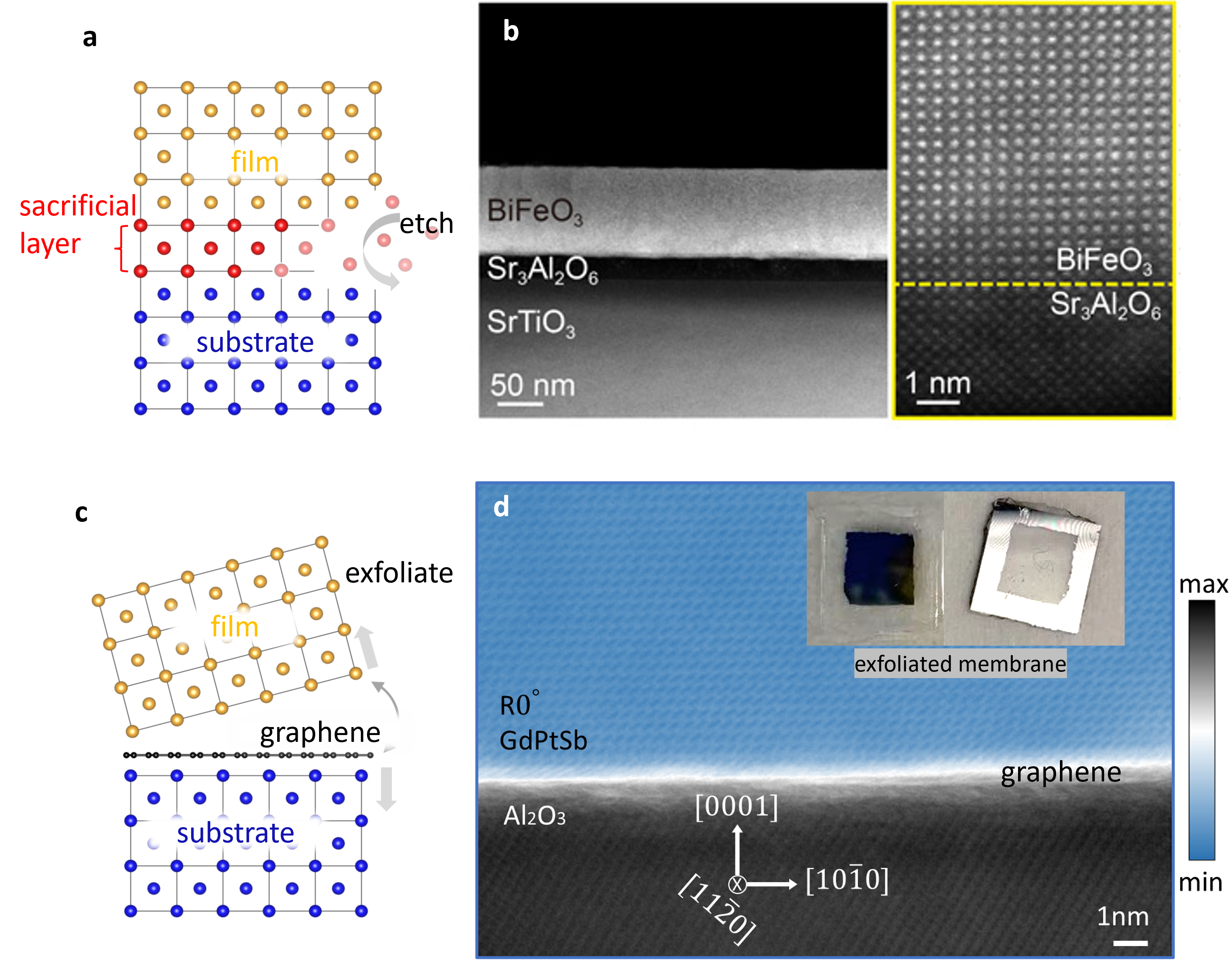
Epitaxial growth and release from a sacrificial etch layer is a leading membrane synthesis strategy (Fig. 2a,b). This approach was first developed for semiconductor membranes, including SiGe membranes by etching the oxide from silicon on insulator (SOI) Roberts et al. (2006), and GaAs/AlAs membranes by selective etches for GaAs or AlAs layers Cheng et al. (2013). It has been extended to other materials that lattice match to semiconductors, including the shape memory alloy Ni2MnGa fabricated via epitaxial growth on AlGaAs and subsequent etching Dong et al. (2004).
New water soluble oxide layers enable the release of free-standing perovskite transition metal oxide membranes. These release layers include (Ca,Sr,Ba)3Al2O6, which allows the lattice parameter to be tuned from 3.819 Å to 4.124 Å Ji et al. (2019); Hong et al. (2020); Chiabrera et al. (2022), SrVO3 Bourlier et al. (2020), and BaO Takahashi and Lippmaa (2020). These layers are typically grown by pulsed laser deposition (PLD)Hong et al. (2020) or molecular beam epitaxy (MBE) Ji et al. (2019). A significant challenge for epitaxial etch release is that not all materials combinations have selective etch chemistries that can etch the lattice matched release layer without damaging the membrane layer.
Remote epitaxy and exfoliation provide an etch-free alternative (Fig. 2c,d). In this approach, an epitaxial film is grown on a graphene (or other 2D material) covered substrate Kim et al. (2017). Epitaxial registry between film and substrate is thought to occur via remote interactions that permeate through graphene Kim et al. (2017); Kong et al. (2018), although a pinhole-seeded mechanism can also produce exfoliatable membranes Manzo et al. (2022). The weak van der Waals interactions of graphene allow film exfoliation to produce a freestanding membrane, similar to exfoliation of vdW materials like graphene and transition metal dichalcogenides. First demonstrated for the compound semiconductors Kim et al. (2017), growth and exfoliation from graphene has been demonstrated for transition metal oxides Kum et al. (2020); Yoon et al. (2022), halide perovskites Jiang et al. (2019), simple metals Lu et al. (2018), and Heusler compounds Du et al. (2021, 2022).
Several challenges exist for remote epitaxy. First, the quality of remote epitaxial film growth and ability to exfoliate depend on the quality of the starting 2D material covered substrate. In most cases, this starting surface is prepared by layer transfer because graphene and other 2D materials cannot be grown directly on arbitrary substrates. This transfer can introduce wrinkles, tears, and interfacial contaminants that introduce defects in the subsequent membrane growth Manzo et al. (2022), and in extreme cases can affect the ability to exfoliate Kim et al. (2021a, b). A cleaner alternative strategy is to use graphene directly grown on the substrate of interest. Recently, epitaxial BaTiO3 membranes were grown on graphene/Ge (110) Dai et al. (2022), where the graphene was grown directly on Ge. Further advancements in remote epitaxy may require the development of graphene growth directly on new substrates of interest.
A second challenge is that the atomic-scale mechanisms for remote epitaxy remain unclear. Clear experimental evidence for a remote mechanism remains elusive. In most experiments, the primary evidence for a remote mechanism is that the films are epitaxial to the underlying substrate (rather than to graphene) and can be exfoliated. Recent in-situ surface science measurements, however, demonstrate that a pinhole-seeded lateral epitaxy mechanism can also produce epitaxial, exfoliatable membranes Manzo et al. (2022). In this growth mode, few nanometer diameter pinholes in the graphene serve as sites for selective nucleation at the substrate, followed by lateral overgrowth and coalescence of a continuous film. Since the pinholes are small and sparse, membranes can still be exfoliated. Moreover, the pinholes are easy to overlook because they do not appear after the graphene transfer step. Instead they only appear immediately prior to film growth because they are created by interfacial oxide desorption at pre-growth sample annealing temperatures.
Careful microscopic measurements at multiple steps during the growth process are required to understand the growth mechanisms on graphene. The development of graphene grown directly on substrates of interest, e.g. graphene on Ge, avoids the interfacial oxide-induced pinholes and may allow the intrinsic mechanisms for remote epitaxy to be tested. Alternative forms of evidence may also shed light on the mechanisms: for GdPtSb films grown on graphene/Al2O3 (0001), a rotated superstructure forms that cannot be explained by pinholes Du et al. (2022). Is this superstructure evidence for an intrinsic remote epitaxy mechanism? A microscopic understanding of the mechanisms, whether intrinsic remote epitaxy or extrinsic pinholes, is required to understand the limits and new applications for epitaxy and exfoliation from graphene.
III.2 Extreme strain manipulation
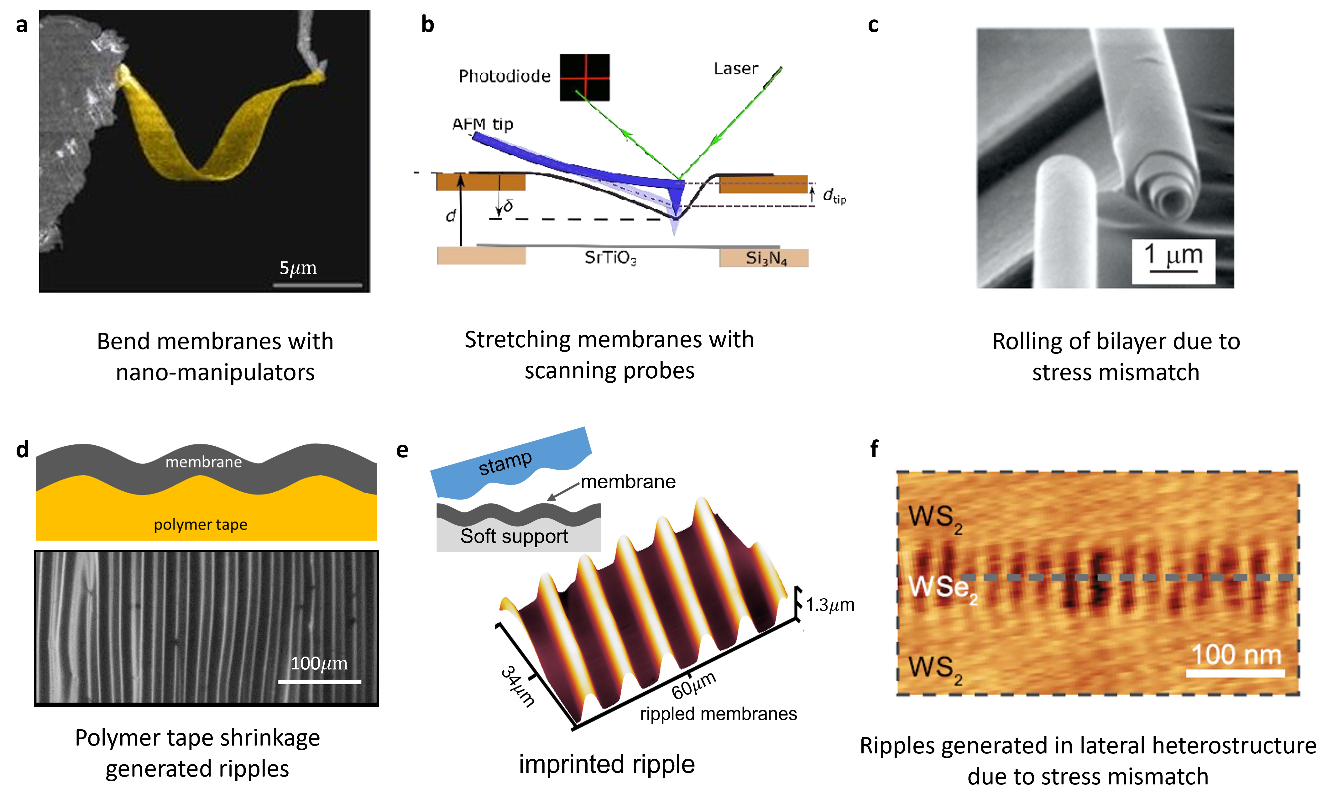
Released membranes enable the application of extreme strains. To date, strain is typically applied via top-down methods. Using micropositioners, strains of 8% have been demonstrated in few nanometer thick (La,Ca)MnO3 membranes in tension Hong et al. (2020), and for BiFeO3 Peng et al. (2020b) and for BaTiO3 membranes Dong et al. (2019) in bending. A flexible polymer handle can aide in the handling of ultrathin membranes, and the use of polymers handles cooled below the glass transition temperature can lock in the desired strain state Hong et al. (2020).
Strain gradients can be produced by bending and rippling. Methods include local bending using a scanning probe or micropositioners Lee (2020); Harbola et al. (2021), Fig. 3 (a,b), rippling via lateral compression on a polymer handle Du et al. (2021); Cai et al. (2022), and transferring membranes to a patterned surface Kang et al. (2021), Fig. 3 (d,e). Local bending by micropositioners have demonstrated elastic recoverable 180 degree bends with 1 micon radius of curvature, as is shown in Fig. 3 (a) Peng et al. (2020b).
Bottom-up strategies provide new opportunities for fine strain gradient control. Strain sharing bilayers, in which one layer is compressive and the other is tensile, spontaneously roll up into nanotubes upon release. This strategy has been successfully implemented to make semiconductor nanotubes Schmidt and Eberl (2001); Huang et al. (2005) and curved oxide membranes Prakash et al. (2022) (Fig. 3 (c)). Another strategy is spontaneous rippling in lattice-mismatched lateral heterostuctures. First implemented for WS2/WSe2 heterostructures, these materials relax via rippling out of plane due to the weak van der Waals interaction with the substrate Xie et al. (2018), as is shown in Fig. 3 (f). We envision similar lateral heterostructures of non vdW membranes, grown by remote epitaxy on graphene, may experience out of plane rippling.
III.3 Why can membranes sustain much larger strains than clamped films or bulk materials?
We offer several possible reasons, based on surface science Zangwill (1988) and the mechanics of 1D metallic whiskers Sears et al. (1954); Herring and Galt (1952); Brenner (1956) and semiconductor and metallic nanowires Wang et al. (2011, 2017); Yue et al. (2011); Li et al. (2021); Deng et al. (2019).
First, membranes are not clamped to a rigid substrate. In epitaxial films, dislocations form when the strain energy exceeds the energy cost to form a misfit dislocation at the film/substrate interface. This criterion, which can be expressed in terms of an energy balance (People and Bean People and Bean (1985), van der Merwe Van Der Merwe (1963)) or a force balance (Matthews and Blakeslee Matthews and Blakeslee (1974)), typically limits strains to %. Otherwise a film relaxes at a critical thickness below one unit cell. For a free-standing membrane, there is no interfacial bonding between film and substrate to create a misfit dislocation. Thus dislocations must nucleate from the bulk or from the top or bottom surface.
Second, ultrathin membranes are dominated by their surfaces. At surface, atoms have decreased local coordination and increased degrees of freedom for relaxation compared to bulk. In response to external stresses, surface atoms can relax out-of-plane or reconstruct in-plane. Surface contributions Müller and Saúl (2004); Liu et al. (2009) are invoked to explain the elasticity of few nanometer diameter nanowires, which can also sustain elastic strains of order Wang et al. (2011, 2017); Yue et al. (2011). Similar arguments may explain why a 6 nm thick (La,Ca)MnO3 membranes can sustain 8% elastic strain, whereas thicker membranes ( nm) undergo fracture below 2% strain Hong et al. (2020).
Interestingly, novel phase transitions and domain reorientations have been observed by transmission electron microscopy in bent ultrathin membranes of the ferroelectric materials BaTiO3 Dong et al. (2019) and BiFeO3 Peng et al. (2020b), and a continuous face centered cubic to body centered tetragonal transition has been detected in few nanometer diameter Cu nanowires Wang et al. (2013). These studies indicate that elastic deformations within the interior of a thin membrane, and not just within the few surface layers, can be different than the bulk. Further microscopic studies are needed in order to understand the relaxations and reconstructions at the surface and near surface region of strained ultrathin membranes.
Third, the mechanisms for generation, motion, and pinning of defects are length scale dependent Uchic et al. (2004). Activation and suppression of these mechanisms has been invoked to explain the size-dependent elastic properties of few micron diameter metallic whiskers Sears et al. (1954); Herring and Galt (1952); Brenner (1956) and micropillars Uchic et al. (2004). Similar arguments may describe the mechanics of membranes at intermediate thicknesses of tens to hundereds of nanometers.
III.4 New developments and challenges in modeling.
An accurate modeling and prediction of the physical properties of strained membranes requires theory and computation at multiple scales. Of central importance is the accurate treatment of the spatially inhomogeneous strain (e.g., strain gradient), which has been challenging to address through first-principles density functional theories (DFT) calculations. This is because inhomogeneous strain often creates non-periodic crystal structure (incommensurate lattice distortion) yet the supercell used in DFT calculation often needs to be periodic. Thanks to the recent advances in the density-functional perturbation theory (DFPT), it is now possible to accurately compute the microscopic response (both linear and non-linear) of a system to an arbitrary inhomogeneous strain. Perhaps the most prominent example is the development of first-principles theory of flexoelectricity Stengel and Vanderbilt (2017) and its application to compute the flexoelectric tensor Dreyer et al. (2018); Schiaffino et al. (2019); Royo and Stengel (2019); Springolo et al. (2021); Royo and Stengel (2022), which can then be utilized to inform the mesoscale/continuum materials modeling Springolo et al. (2021).
Despite these exciting developments, significant challenges still remain. For example, the properties of strained membrane, like most practical materials, depend on the formation and evolution of mesoscale patterns (e.g., magnetic/ferroelectric/ferroelastic domains, electronic phase separation) at finite temperature, which go beyond the capability of conventional DFT calculations. However, research into the prediction of mesoscale pattern formation under extreme strain condition is still at its early stage, with many open questions remain. Take the ferroelectrics as an example, large bending can significantly change the bandgap of the domain wall Eliseev et al. (2012) and hence lead to redistribution of the ionic and electronic defects and even an insulator-to-metal transition Stolichnov et al. (2015). How does the strain-induced ionic/electronic defect redistribution interact with the domain structure evolution under extreme strain condition Deng et al. (2019)? How does the defect distribution influence the strain-induced ferroelectric/ferroelastic phase transition? How to disentangle the contribution of flexoelectricity, piezoelectricity, and electrostriction to the mesoscale pattern formation? In addition to these fundamental challenges, there also exist technical challenges in different computational methods.
Modern atomistic methods such as effective Hamiltonian-based methodsZhong et al. (1994); Bellaiche et al. (2000); Lai et al. (2006); Nahas et al. (2020) and second-principles calculations Wojdeł et al. (2013); Wojdeł and Iniguez (2014); Garcia-Fernandez et al. (2016) can predict the mesoscale pattern formation with atom-resolved spatial resolution, and permits taking input directly from DFT calculations without the need of parameterization. However, it is still challenging to consider the realistic mechanical boundary conditions for the application of strain and strain gradient (Fig. 3) and their application to practical-sized (e.g., hundreds of micrometers to millimeters) materials systems currently would consume too much computational resources to be realistic.
Mesoscale materials modeling methods such as phase-field modeling cannot predict pattern formation and evolution at the scale below one unit cell, but can conveniently consider the complexity arising from the actual mechanical boundary condition upon the application of strain (gradient) Deng et al. (2019); Li et al. (2021); Park et al. (2022); Peng et al. (2020b); Dong et al. (2019), and incorporate the role of 0D (point defects such as oxygen vacancies Deng et al. (2019)), 1D (dislocations Zhuo et al. (2022)), 2D (grain boundaries Dai et al. (2021); Choudhury et al. (2007); Hu et al. (2019)), and 3D (e.g., precipitates Zhao et al. (2021) and cracks Liu et al. (2018)). In particular, the phase-field model has the additional versatility of modeling the formation and co-evolution of different types of coupled patterns, for example, the coupled magnetic and structural domains Ohmer et al. (2022); Huang et al. (2015); Wu et al. (2011). With input from ab initio and/or experimental measurements, the predicted mesoscale patterns can often be utilized for a side-by-side comparison to experiments for not only understanding and interpreting the results, but also provide insights into how to access these patterns and manipulate them for realizing exotic phenomena or enhanced responses Qiu et al. (2020); Pan et al. (2019, 2021).
IV Outlook: beyond static strains
Large strains and strain gradients provide unique opportunities for inducing new properties in membranes of quantum materials. This Perspective highlighted static strain tuning of magnetism, superconductivity, ferroelectricity, and topological states.
Exciting opportunities also lie in dynamic and nonequilibirum properties. Nonlinear phononics, in which ultrafast optical pulses resonantly excite phonon modes, is a powerful approach for revealing nonequilibrium properties that arise from photon-phonon-spin or photon-phonon-electron couplings. Examples include ultrafast antiferromagnetic-ferrimagnetic switching Disa et al. (2020), metastable ferroelectricity Nova et al. (2019), and possible nonequilibrium superconductivity Budden et al. (2021). The general applicability of nonlinear phononics, however, is limited since these complex couplings are often weak, difficult to tune, and difficult to apply beyond a narrow set of materials that obey the required symmetry constraints. We anticipate the strong symmetry-breaking strains and strain gradients in membranes may solve this challenge, by enhancing the quasiparticle coupling strengths via strain, and breaking symmetries to activate new phonon modes for resonant excitation. The absence of substrate clamping is also beneficial since larger amplitude lattice vibrations can be accessed. Strain and strain gradients, both in static and dynamic forms, provide power tuning knobs for unleashing hidden properties in quantum materials membranes.
V Acknowledgements
We thank Cyrus Dreyer, Jun Xiao, Daniel Rhodes, Ying Wang, and Uwe Bergmann for discussions. JKK and DD acknowledge the Air Force Office of Scientific Research (FA9550-21-0127) and the National Science Foundation (DMR-1752797). All authors acknowledge the National Science Foundation through the University of Wisconsin Materials Research Science and Engineering Center (MRSEC) Grant No. DMR-1720415.
References
- Ruf et al. (2021) J. P. Ruf, H. Paik, N. J. Schreiber, H. P. Nair, L. Miao, J. K. Kawasaki, J. N. Nelson, B. D. Faeth, Y. Lee, B. H. Goodge, et al., Nature Communications 12, 1 (2021).
- Schlom et al. (2007) D. G. Schlom, L.-Q. Chen, C.-B. Eom, K. M. Rabe, S. K. Streiffer, and J.-M. Triscone, Annual Review of Materials Research 37, 589 (2007).
- Song et al. (2020) X. Song, C. Xiong, F. Zhang, Y. Nie, and Y. Li, Materials Letters 259, 126914 (2020).
- Matthews and Blakeslee (1974) J. Matthews and A. Blakeslee, Journal of Crystal growth 27, 118 (1974).
- People and Bean (1985) R. People and J. Bean, Applied Physics Letters 47, 322 (1985).
- Van Der Merwe (1963) J. H. Van Der Merwe, Journal of Applied Physics 34, 123 (1963).
- Hong et al. (2020) S. S. Hong, M. Gu, M. Verma, V. Harbola, B. Y. Wang, D. Lu, A. Vailionis, Y. Hikita, R. Pentcheva, J. M. Rondinelli, et al., Science 368, 71 (2020).
- Dong et al. (2019) G. Dong, S. Li, M. Yao, Z. Zhou, Y.-Q. Zhang, X. Han, Z. Luo, J. Yao, B. Peng, Z. Hu, et al., Science 366, 475 (2019).
- Du et al. (2021) D. Du, S. Manzo, C. Zhang, V. Saraswat, K. T. Genser, K. M. Rabe, P. M. Voyles, M. S. Arnold, and J. K. Kawasaki, Nature communications 12, 1 (2021).
- Kim et al. (2017) Y. Kim, S. S. Cruz, K. Lee, B. O. Alawode, C. Choi, Y. Song, J. M. Johnson, C. Heidelberger, W. Kong, S. Choi, et al., Nature 544, 340 (2017).
- Kum et al. (2020) H. S. Kum, H. Lee, S. Kim, S. Lindemann, W. Kong, K. Qiao, P. Chen, J. Irwin, J. H. Lee, S. Xie, et al., Nature 578, 75 (2020).
- Du et al. (2022) D. Du, T. Jung, S. Manzo, Z. LaDuca, X. Zheng, K. Su, V. Saraswat, J. McChesney, M. S. Arnold, and J. K. Kawasaki, Nano Letters 22, 8647 (2022).
- Yoon et al. (2022) H. Yoon, T. K. Truttmann, F. Liu, B. E. Matthews, S. Choo, Q. Su, V. Saraswat, S. Manzo, M. S. Arnold, M. E. Bowden, et al., arXiv preprint arXiv:2206.09094 (2022).
- Dai et al. (2022) L. Dai, J. Zhao, J. Li, B. Chen, S. Zhai, Z. Xue, Z. Di, B. Feng, Y. Sun, Y. Luo, et al., Nature Communications 13, 1 (2022).
- Si et al. (2016) C. Si, Z. Sun, and F. Liu, Nanoscale 8, 3207 (2016).
- Peng et al. (2020a) Z. Peng, X. Chen, Y. Fan, D. J. Srolovitz, and D. Lei, Light: Science & Applications 9, 1 (2020a).
- Zhang et al. (2018a) J. Zhang, C. Ji, Y. Shangguan, B. Guo, J. Wang, F. Huang, X. Lu, and J. Zhu, Physical Review B 98, 195133 (2018a).
- Casper et al. (2012) F. Casper, T. Graf, S. Chadov, B. Balke, and C. Felser, Semiconductor Science and Technology 27, 063001 (2012).
- Bibes and Barthelemy (2007) M. Bibes and A. Barthelemy, IEEE transactions on electron devices 54, 1003 (2007).
- Bibes et al. (2011) M. Bibes, J. E. Villegas, and A. Barthélémy, Advances in Physics 60, 5 (2011).
- Eliseev et al. (2011) E. A. Eliseev, M. Glinchuk, V. Khist, V. Skorokhod, R. Blinc, and A. Morozovska, Physical Review B 84, 174112 (2011).
- Lukashev and Sabirianov (2010) P. Lukashev and R. F. Sabirianov, Physical Review B 82, 094417 (2010).
- Eliseev et al. (2009) E. A. Eliseev, A. N. Morozovska, M. D. Glinchuk, and R. Blinc, Physical Review B 79, 165433 (2009).
- Zhang et al. (2021) Y. Zhang, J. Liu, Y. Dong, S. Wu, J. Zhang, J. Wang, J. Lu, A. Rückriegel, H. Wang, R. Duine, et al., Physical Review Letters 127, 117204 (2021).
- Liu et al. (2022) L. Liu, W. Chen, and Y. Zheng, Physical Review Letters 128, 257201 (2022).
- Edström et al. (2022) A. Edström, D. Amoroso, S. Picozzi, P. Barone, and M. Stengel, Physical Review Letters 128, 177202 (2022).
- Yanes et al. (2019) R. Yanes, F. Garcia-Sanchez, R. Luis, E. Martinez, V. Raposo, L. Torres, and L. Lopez-Diaz, Applied Physics Letters 115, 132401 (2019).
- Liu et al. (2019) Y. Liu, X. Huo, S. Xuan, and H. Yan, Journal of Magnetism and Magnetic Materials 492, 165659 (2019).
- Gorshkov et al. (2022) I. O. Gorshkov, R. V. Gorev, M. V. Sapozhnikov, and O. G. Udalov, ACS Applied Electronic Materials 4, 3205 (2022).
- Xu et al. (2020) R. Xu, J. Huang, E. S. Barnard, S. S. Hong, P. Singh, E. K. Wong, T. Jansen, V. Harbola, J. Xiao, B. Y. Wang, et al., Nature communications 11, 1 (2020).
- Pesquera et al. (2020) D. Pesquera, E. Parsonnet, A. Qualls, R. Xu, A. J. Gubser, J. Kim, Y. Jiang, G. Velarde, Y.-L. Huang, H. Y. Hwang, et al., Advanced Materials 32, 2003780 (2020).
- Kogan (1964) S. M. Kogan, Soviet Physics-Solid State 5, 2069 (1964).
- Zubko et al. (2013) P. Zubko, G. Catalan, and A. K. Tagantsev (2013).
- Cross (2006) L. E. Cross, Journal of Materials Science 41, 53 (2006).
- Indenbom et al. (1981) V. Indenbom, E. Loginov, and M. Osipov, Kristallografiya 26, 1157 (1981).
- Ma and Cross (2001) W. Ma and L. E. Cross, Applied Physics Letters 78, 2920 (2001).
- Ma and Cross (2005) W. Ma and L. E. Cross, Applied Physics Letters 86, 072905 (2005).
- Zabalo and Stengel (2021) A. Zabalo and M. Stengel, Physical Review Letters 126, 127601 (2021).
- Du et al. (2019) D. Du, A. Lim, C. Zhang, P. J. Strohbeen, E. H. Shourov, F. Rodolakis, J. L. McChesney, P. Voyles, D. C. Fredrickson, and J. K. Kawasaki, APL Materials 7, 121107 (2019).
- Peng et al. (2020b) B. Peng, R.-C. Peng, Y.-Q. Zhang, G. Dong, Z. Zhou, Y. Zhou, T. Li, Z. Liu, Z. Luo, S. Wang, et al., Science advances 6, eaba5847 (2020b).
- Engelmann et al. (2013) J. Engelmann, V. Grinenko, P. Chekhonin, W. Skrotzki, D. Efremov, S. Oswald, K. Iida, R. Hühne, J. Hänisch, M. Hoffmann, et al., Nature communications 4, 1 (2013).
- Tarantini et al. (2011) C. Tarantini, A. Gurevich, J. Jaroszynski, F. Balakirev, E. Bellingeri, I. Pallecchi, C. Ferdeghini, B. Shen, H. Wen, and D. Larbalestier, Physical Review B 84, 184522 (2011).
- Okabe et al. (2010) H. Okabe, N. Takeshita, K. Horigane, T. Muranaka, and J. Akimitsu, Physical Review B 81, 205119 (2010).
- Mandal et al. (2017) S. Mandal, P. Zhang, S. Ismail-Beigi, and K. Haule, Physical review letters 119, 067004 (2017).
- Wang et al. (2012) Q.-Y. Wang, Z. Li, W.-H. Zhang, Z.-C. Zhang, J.-S. Zhang, W. Li, H. Ding, Y.-B. Ou, P. Deng, K. Chang, et al., Chinese Physics Letters 29, 037402 (2012).
- Lee et al. (2014) J. Lee, F. Schmitt, R. Moore, S. Johnston, Y.-T. Cui, W. Li, M. Yi, Z. Liu, M. Hashimoto, Y. Zhang, et al., Nature 515, 245 (2014).
- Tan et al. (2013) S. Tan, Y. Zhang, M. Xia, Z. Ye, F. Chen, X. Xie, R. Peng, D. Xu, Q. Fan, H. Xu, et al., Nature materials 12, 634 (2013).
- Locquet et al. (1998) J.-P. Locquet, J. Perret, J. Fompeyrine, E. Mächler, J. W. Seo, and G. Van Tendeloo, Nature 394, 453 (1998).
- Bozovic et al. (2002) I. Bozovic, G. Logvenov, I. Belca, B. Narimbetov, and I. Sveklo, Physical review letters 89, 107001 (2002).
- Edge et al. (2015) J. M. Edge, Y. Kedem, U. Aschauer, N. A. Spaldin, and A. V. Balatsky, Physical Review Letters 115, 247002 (2015).
- Ahadi et al. (2019) K. Ahadi, L. Galletti, Y. Li, S. Salmani-Rezaie, W. Wu, and S. Stemmer, Science advances 5, eaaw0120 (2019).
- Müller and Burkard (1979) K. A. Müller and H. Burkard, Physical Review B 19, 3593 (1979).
- Rytz et al. (1980) D. Rytz, U. Höchli, and H. Bilz, Physical Review B 22, 359 (1980).
- Yip (2014) S. Yip, Annu. Rev. Condens. Matter Phys. 5, 15 (2014).
- Gor’kov and Rashba (2001) L. P. Gor’kov and E. I. Rashba, Physical Review Letters 87, 037004 (2001).
- Zhang et al. (2018b) P. Zhang, K. Yaji, T. Hashimoto, Y. Ota, T. Kondo, K. Okazaki, Z. Wang, J. Wen, G. Gu, H. Ding, et al., Science 360, 182 (2018b).
- Wang et al. (2018) D. Wang, L. Kong, P. Fan, H. Chen, S. Zhu, W. Liu, L. Cao, Y. Sun, S. Du, J. Schneeloch, et al., Science 362, 333 (2018).
- Machida et al. (2019) T. Machida, Y. Sun, S. Pyon, S. Takeda, Y. Kohsaka, T. Hanaguri, T. Sasagawa, and T. Tamegai, Nature materials 18, 811 (2019).
- Lohani et al. (2020) H. Lohani, T. Hazra, A. Ribak, Y. Nitzav, H. Fu, B. Yan, M. Randeria, and A. Kanigel, Physical Review B 101, 245146 (2020).
- Wang et al. (2015) Z. Wang, P. Zhang, G. Xu, L. Zeng, H. Miao, X. Xu, T. Qian, H. Weng, P. Richard, A. V. Fedorov, et al., Physical Review B 92, 115119 (2015).
- Lin et al. (2010) H. Lin, L. A. Wray, Y. Xia, S. Xu, S. Jia, R. J. Cava, A. Bansil, and M. Z. Hasan, Nature materials 9, 546 (2010).
- Chadov et al. (2010) S. Chadov, X. Qi, J. Kübler, G. H. Fecher, C. Felser, and S. C. Zhang, Nature materials 9, 541 (2010).
- Nakajima et al. (2015) Y. Nakajima, R. Hu, K. Kirshenbaum, A. Hughes, P. Syers, X. Wang, K. Wang, R. Wang, S. R. Saha, D. Pratt, et al., Science advances 1, e1500242 (2015).
- Singh et al. (2020) A. K. Singh, S. Ramarao, and S. C. Peter, APL Materials 8, 060903 (2020).
- Al-Sawai et al. (2010) W. Al-Sawai, H. Lin, R. Markiewicz, L. Wray, Y. Xia, S.-Y. Xu, M. Hasan, and A. Bansil, Physical Review B 82, 125208 (2010).
- Xiao et al. (2010) D. Xiao, Y. Yao, W. Feng, J. Wen, W. Zhu, X.-Q. Chen, G. M. Stocks, and Z. Zhang, Physical review letters 105, 096404 (2010).
- Jiang et al. (2017) Y. Jiang, J. Mao, J. Duan, X. Lai, K. Watanabe, T. Taniguchi, and E. Y. Andrei, Nano letters 17, 2839 (2017).
- Kang et al. (2021) D.-H. Kang, H. Sun, M. Luo, K. Lu, M. Chen, Y. Kim, Y. Jung, X. Gao, S. J. Parluhutan, J. Ge, et al., Nature Communications 12, 1 (2021).
- Tang and Fu (2014) E. Tang and L. Fu, Nature Physics 10, 964 (2014).
- Armitage et al. (2018) N. Armitage, E. Mele, and A. Vishwanath, Reviews of Modern Physics 90, 015001 (2018).
- Roberts et al. (2006) M. M. Roberts, L. J. Klein, D. E. Savage, K. A. Slinker, M. Friesen, G. Celler, M. A. Eriksson, and M. G. Lagally, Nature materials 5, 388 (2006).
- Cheng et al. (2013) C.-W. Cheng, K.-T. Shiu, N. Li, S.-J. Han, L. Shi, and D. K. Sadana, Nature communications 4, 1 (2013).
- Dong et al. (2004) J. Dong, J. Xie, J. Lu, C. Adelmann, C. Palmstrøm, J. Cui, Q. Pan, T. Shield, R. James, and S. McKernan, Journal of applied physics 95, 2593 (2004).
- Ji et al. (2019) D. Ji, S. Cai, T. R. Paudel, H. Sun, C. Zhang, L. Han, Y. Wei, Y. Zang, M. Gu, Y. Zhang, et al., Nature 570, 87 (2019).
- Chiabrera et al. (2022) F. M. Chiabrera, S. Yun, Y. Li, R. T. Dahm, H. Zhang, C. K. Kirchert, D. V. Christensen, F. Trier, T. S. Jespersen, and N. Pryds, Annalen der Physik 534, 2200084 (2022).
- Bourlier et al. (2020) Y. Bourlier, B. Berini, M. Frégnaux, A. Fouchet, D. Aureau, and Y. Dumont, ACS applied materials & interfaces 12, 8466 (2020).
- Takahashi and Lippmaa (2020) R. Takahashi and M. Lippmaa, ACS applied materials & interfaces 12, 25042 (2020).
- Kong et al. (2018) W. Kong, H. Li, K. Qiao, Y. Kim, K. Lee, Y. Nie, D. Lee, T. Osadchy, R. J. Molnar, D. K. Gaskill, et al., Nature materials 17, 999 (2018).
- Manzo et al. (2022) S. Manzo, P. J. Strohbeen, Z. H. Lim, V. Saraswat, D. Du, S. Xu, N. Pokharel, L. J. Mawst, M. S. Arnold, and J. K. Kawasaki, Nature communications 13, 1 (2022).
- Jiang et al. (2019) J. Jiang, X. Sun, X. Chen, B. Wang, Z. Chen, Y. Hu, Y. Guo, L. Zhang, Y. Ma, L. Gao, et al., Nature communications 10, 1 (2019).
- Lu et al. (2018) Z. Lu, X. Sun, W. Xie, A. Littlejohn, G.-C. Wang, S. Zhang, M. A. Washington, and T.-M. Lu, Nanotechnology 29, 445702 (2018).
- Kim et al. (2021a) H. Kim, J. C. Kim, Y. Jeong, J. Yu, K. Lu, D. Lee, N. Kim, H. Y. Jeong, J. Kim, and S. Kim, Journal of Applied Physics 130, 174901 (2021a).
- Kim et al. (2021b) H. Kim, K. Lu, Y. Liu, H. S. Kum, K. S. Kim, K. Qiao, S.-H. Bae, S. Lee, Y. J. Ji, K. H. Kim, et al., ACS nano 15, 10587 (2021b).
- Harbola et al. (2021) V. Harbola, S. Crossley, S. S. Hong, D. Lu, Y. A. Birkholzer, Y. Hikita, and H. Y. Hwang, Nano letters 21, 2470 (2021).
- Prakash et al. (2022) D. J. Prakash, Y. Chen, M. L. Debasu, D. E. Savage, C. Tangpatjaroen, C. Deneke, A. Malachias, A. D. Alfieri, O. Elleuch, K. Lekhal, et al., Small 18, 2105424 (2022).
- Xie et al. (2018) S. Xie, L. Tu, Y. Han, L. Huang, K. Kang, K. U. Lao, P. Poddar, C. Park, D. A. Muller, R. A. DiStasio Jr, et al., Science 359, 1131 (2018).
- Lee (2020) D. Lee, Apl Materials 8, 090901 (2020).
- Cai et al. (2022) S. Cai, Y. Lun, D. Ji, P. Lv, L. Han, C. Guo, Y. Zang, S. Gao, Y. Wei, M. Gu, et al. (2022).
- Schmidt and Eberl (2001) O. G. Schmidt and K. Eberl, Nature 410, 168 (2001).
- Huang et al. (2005) M. Huang, C. Boone, M. Roberts, D. E. Savage, M. G. Lagally, N. Shaji, H. Qin, R. Blick, J. A. Nairn, and F. Liu, Advanced Materials 17, 2860 (2005).
- Zangwill (1988) A. Zangwill, Physics at surfaces (Cambridge university press, 1988).
- Sears et al. (1954) G. Sears, A. Gatti, and R. Fullman, Acta Metallurgica 2, 727 (1954).
- Herring and Galt (1952) C. Herring and J. Galt, Physical Review 85, 1060 (1952).
- Brenner (1956) S. S. Brenner, Journal of applied physics 27, 1484 (1956).
- Wang et al. (2011) Y.-B. Wang, L.-F. Wang, H. J. Joyce, Q. Gao, X.-Z. Liao, Y.-W. Mai, H. H. Tan, J. Zou, S. P. Ringer, H.-J. Gao, et al., Advanced Materials 23, 1356 (2011).
- Wang et al. (2017) S. Wang, Z. Shan, and H. Huang, Advanced Science 4, 1600332 (2017).
- Yue et al. (2011) Y. Yue, P. Liu, Z. Zhang, X. Han, and E. Ma, Nano letters 11, 3151 (2011).
- Li et al. (2021) Y. Li, K. Chu, C. Liu, P. Jiang, K. Qu, P. Gao, J. Wang, F. Ren, Q. Sun, L. Chen, et al., Proceedings of the National Academy of Sciences 118, e2025255118 (2021).
- Deng et al. (2019) Y. Deng, C. Gammer, J. Ciston, P. Ercius, C. Ophus, K. Bustillo, C. Song, R. Zhang, D. Wu, Y. Du, et al., Acta Materialia 181, 501 (2019).
- Müller and Saúl (2004) P. Müller and A. Saúl, Surface Science Reports 54, 157 (2004).
- Liu et al. (2009) X. Liu, J. Li, Z. Zhou, L. Yang, Z. Ma, G. Xie, Y. Pan, and C. Q. Sun, Applied Physics Letters 94, 131902 (2009).
- Wang et al. (2013) L. Wang, P. Liu, P. Guan, M. Yang, J. Sun, Y. Cheng, A. Hirata, Z. Zhang, E. Ma, M. Chen, et al., Nature communications 4, 1 (2013).
- Uchic et al. (2004) M. D. Uchic, D. M. Dimiduk, J. N. Florando, and W. D. Nix, Science 305, 986 (2004).
- Stengel and Vanderbilt (2017) M. Stengel and D. Vanderbilt, in Flexoelectricity In Solids: From Theory To Applications (World Scientific, 2017), pp. 31–110.
- Dreyer et al. (2018) C. E. Dreyer, M. Stengel, and D. Vanderbilt, Physical Review B 98, 075153 (2018).
- Schiaffino et al. (2019) A. Schiaffino, C. E. Dreyer, D. Vanderbilt, and M. Stengel, Physical Review B 99, 085107 (2019).
- Royo and Stengel (2019) M. Royo and M. Stengel, Physical Review X 9, 021050 (2019).
- Springolo et al. (2021) M. Springolo, M. Royo, and M. Stengel, Physical review letters 127, 216801 (2021).
- Royo and Stengel (2022) M. Royo and M. Stengel, Physical Review B 105, 064101 (2022).
- Eliseev et al. (2012) E. A. Eliseev, A. N. Morozovska, Y. Gu, A. Y. Borisevich, L.-Q. Chen, V. Gopalan, and S. V. Kalinin, Physical Review B 86, 085416 (2012).
- Stolichnov et al. (2015) I. Stolichnov, L. Feigl, L. J. McGilly, T. Sluka, X.-K. Wei, E. Colla, A. Crassous, K. Shapovalov, P. Yudin, A. K. Tagantsev, et al., Nano Letters 15, 8049 (2015).
- Zhong et al. (1994) W. Zhong, D. Vanderbilt, and K. Rabe, Physical Review Letters 73, 1861 (1994).
- Bellaiche et al. (2000) L. Bellaiche, A. García, and D. Vanderbilt, Physical Review Letters 84, 5427 (2000).
- Lai et al. (2006) B.-K. Lai, I. Ponomareva, I. Naumov, I. Kornev, H. Fu, L. Bellaiche, and G. Salamo, Physical review letters 96, 137602 (2006).
- Nahas et al. (2020) Y. Nahas, S. Prokhorenko, J. Fischer, B. Xu, C. Carrétéro, S. Prosandeev, M. Bibes, S. Fusil, B. Dkhil, V. Garcia, et al., Nature 577, 47 (2020).
- Wojdeł et al. (2013) J. C. Wojdeł, P. Hermet, M. P. Ljungberg, P. Ghosez, and J. Iniguez, Journal of Physics: Condensed Matter 25, 305401 (2013).
- Wojdeł and Iniguez (2014) J. C. Wojdeł and J. Iniguez, Physical Review Letters 112, 247603 (2014).
- Garcia-Fernandez et al. (2016) P. Garcia-Fernandez, J. C. Wojdeł, J. Iniguez, and J. Junquera, Physical Review B 93, 195137 (2016).
- Park et al. (2022) S. Park, B. Wang, T. Yang, J. Kim, S. Saremi, W. Zhao, B. Guzelturk, A. Sood, C. Nyby, M. Zajac, et al., Nano Letters (2022).
- Zhuo et al. (2022) F. Zhuo, X. Zhou, S. Gao, M. Höfling, F. Dietrich, P. B. Groszewicz, L. Fulanović, P. Breckner, A. Wohninsland, B.-X. Xu, et al., Nature communications 13, 1 (2022).
- Dai et al. (2021) M. Dai, M. F. Demirel, Y. Liang, and J.-M. Hu, npj Computational Materials 7, 1 (2021).
- Choudhury et al. (2007) S. Choudhury, Y. Li, C. Krill Iii, and L. Chen, Acta materialia 55, 1415 (2007).
- Hu et al. (2019) C.-C. Hu, Z. Zhang, T.-N. Yang, Y.-G. Shi, X.-X. Cheng, J.-J. Ni, J.-G. Hao, W.-F. Rao, and L.-Q. Chen, Applied physics letters 115, 162402 (2019).
- Zhao et al. (2021) C. Zhao, S. Gao, T. Yang, M. Scherer, J. Schultheiß, D. Meier, X. Tan, H.-J. Kleebe, L.-Q. Chen, J. Koruza, et al., Advanced Materials 33, 2102421 (2021).
- Liu et al. (2018) Z. Liu, J. Liu, M. D. Biegalski, J.-M. Hu, S. Shang, Y. Ji, J. Wang, S. Hsu, A. Wong, M. Cordill, et al., Nature communications 9, 1 (2018).
- Ohmer et al. (2022) D. Ohmer, M. Yi, O. Gutfleisch, and B.-X. Xu, International Journal of Solids and Structures 238, 111365 (2022).
- Huang et al. (2015) H. Huang, X. Ma, J. Wang, Z. Liu, W. He, and L. Chen, Acta Materialia 83, 333 (2015).
- Wu et al. (2011) P. Wu, X. Ma, J. Zhang, and L. Chen, Philosophical Magazine 91, 2102 (2011).
- Qiu et al. (2020) C. Qiu, B. Wang, N. Zhang, S. Zhang, J. Liu, D. Walker, Y. Wang, H. Tian, T. R. Shrout, Z. Xu, et al., Nature 577, 350 (2020).
- Pan et al. (2019) H. Pan, F. Li, Y. Liu, Q. Zhang, M. Wang, S. Lan, Y. Zheng, J. Ma, L. Gu, Y. Shen, et al., Science 365, 578 (2019).
- Pan et al. (2021) H. Pan, S. Lan, S. Xu, Q. Zhang, H. Yao, Y. Liu, F. Meng, E.-J. Guo, L. Gu, D. Yi, et al., Science 374, 100 (2021).
- Disa et al. (2020) A. S. Disa, M. Fechner, T. F. Nova, B. Liu, M. Först, D. Prabhakaran, P. G. Radaelli, and A. Cavalleri, Nature Physics 16, 937 (2020).
- Nova et al. (2019) T. Nova, A. Disa, M. Fechner, and A. Cavalleri, Science 364, 1075 (2019).
- Budden et al. (2021) M. Budden, T. Gebert, M. Buzzi, G. Jotzu, E. Wang, T. Matsuyama, G. Meier, Y. Laplace, D. Pontiroli, M. Riccò, et al., Nature Physics 17, 611 (2021).