Tunable Electron Transport in Defect-Engineered PdSe2
Abstract
Tuning the ambipolar behavior in charge carrier transport via defect-engineering is crucial for achieving high mobility transistors for nonlinear logic circuits. Here, we present the electric-field tunable electron and hole transport in a microchannel device consisting of highly air-stable van der Waals (vdW) noble metal dichalcogenide (NMDC), PdSe2, as an active layer. Pristine bulk PdSe2 constitutes Se surface vacancy defects created during the growth or exfoliation process and offers an ambipolar transfer characteristics with a slight electron dominance recorded in field-effect transistor (FET) characteristics showing an ON/OFF ratio 10 and electron mobility 21 cm2/V.s. However, transfer characteristics of PdSe2 can be tuned to a hole-dominated transport while using hydrochloric acid (HCl) as a p-type dopant. On the other hand, the chelating agent EDTA, being a strong electron donor, enhances the electron-dominance in PdSe2 channel. In addition, p-type behavior with a 100 times higher ON/OFF ratio is obtained while cooling the sample down to 10 K. Low-temperature angle-resolved photoemission spectroscopy resembles the p-type band structure of PdSe2 single crystal. Also, first principle density functional theory calculations justify the tunability observed in PdSe2 as a result of defect-engineering. Such a defect-sensitive ambipolar vdW architecture may open up new possibilities towards future CMOS (Complementary Metal-Oxide-Semiconductor) device fabrications and high performance integrated circuits.
1 Introduction
Performance of a FET based on downscaled two-dimensional (2D) vdW semiconductors like transition metal dichalcogenides (TMDCs) (e.g. MoS2, WS2, MoSe2 etc.) as channel depends on the layer’s chemical and environmental stability 1, 2, 3. In TMDCs, aging effects like gradual oxidation at the TM edges of a micromechanically exfoliated flake transferred from the bulk crystal or at the grain boundaries of a large area sheet hinders its enduring applications in nanoelectronics and optoelectronics. As it happens, easy dissociation of molecular oxygen at the TM edge (e.g. Mo edge in MoS2) with low barrier energy (close to 0.3 eV) compared to its protection at the surface (1.5 eV on the MoS2 surface) makes the layer more susceptible to wrinkle formation, morphological variation with time. Nonetheless, for the fundamental research concerning electronic/optoelectronic devices, utilizing the standard crystal-growth techniques like chemical vapor deposition (CVD) or chemical vapor transport (CVT) 4, 5, TMDC flakes/nanostructures can be grown on the conventional SiO2/Si substrate and contacted with metal electrodes using lithography, followed by electron/hole transport measurements in the FET geometry depending on the band structure and doping profile. Also, highly disparate atomic layers can be stacked together, e.g. graphene and MoS2, to form vdW heterostructures without any constraint of lattice matching 6, 7. Surface charge transfer using donor/acceptor molecule for suitable doping in few-layer TMDC, like WSe2, may result in improved ON/OFF ratio and higher mobility than the pristine samples 8. Besides, hydracid treatment in monolayer MoSe2 reduces the Se-vacancies by passivation, and thereby, enhances the photoluminescence 9. Similarly, using ethylenediaminetetra acetic acid (EDTA) as electron donor, repairing of single/double Se vacancies can be achieved in single layer of MoSe2, and as a result of which several times of increment in the carrier density can be observed 10.
Although notable advancement has been perceived in the device electronics with defect-engineered surfaces of TMDC, researchers got involved in exploring a new family of 2D vdW semiconducting materials, noble metal dichalcogenides (NMDCs) with the stoichiometry (metal M = Pt, Pd, and chalcogen X = S, Se, Te) which may provide superior air-stability with similar or enhanced FET performance 11. In contrast to the conventional Group 6 TMDCs, NMDCs with group 10 elements possess largely occupied d-orbitals (more than half-filled) of the noble metals and highly hybridized pz orbitals of the chalcogen atoms which may lead to strong interlayer coupling as well as layer dependent band-gap, as observed in one of the compound from NMDC family, PtS2 (0.2 eV in bulk and 1.6 eV in the monolayer) 12, 13, 14. Additionally, it has been predicted that coordinatively unsaturated noble metal, like Pd, will have much higher O2 adsorption energy barrier ( 1.2 eV) than Group 6 elements which might be the reason for high air-stability at the edges 13, 15. Recent experimental study has confirmed that the device performance of PtSe2 FET remains nearly unchanged after 5 months of air-exposure 15. Apart from the air-stability and layer dependence, the electronic properties of these materials vary extensively due to surface vacancy defects introduced during the growth and exfoliation process or can be further tuned by doping 16, 17, 18, 19. Altogether, air-stable NMDCs in the reduced dimension may exhibit better device performance and tunability via defect engineering for future applications in logic circuits 20.
Recently, palladium diselenide (PdSe2), a Group 10 NMDC has been explored and recognized as a highly air-stable layered material with a unique puckered pentagonal morphology 13. Usually, puckered configuration exhibits novel anisotropic properties which is rarely found in the family of 2D materials. Unlike the conventional TMDCs and other NMDCs, in the unit cell of PdSe2, each Pd atom is surrounded by four Se-Se intralayer dimers and thereby forms a PdSe4 unit. This type of structure makes the crystal more defect-sensitive due to the kinetic barrier of the Se-vacancy diffusion which is much lower than any other TMDC resulting in a structural distortion by the symmetry breaking of Se-Se intralayer bonds 21, 22. This defect-sensitivity potentially enriches electronic transport as well as phase change engineering. Previously, first-principle calculations predicted the tunability of layered PdSe2 due to surface vacancy defects 16, 23. But the experimental regime of defect engineering in PdSe2 is still unexplored.
Here, we report tunable electronic transport properties of defect-engineered bulk layer of vdW material PdSe2. Being a low band gap semiconductor in pristine bulk (Eg 0.3 - 0.4 eV), PdSe2 shows consistent ambipolar transfer characteristics with ON/OFF ratio 10 and electron mobility 21 cm2/V.s in the ambient condition while using as channel in the FET. The mobility value is quite large in comparison to TMDCs like MoS2 24. By lowering the temperature the ON/OFF ratio gets improved more than 100 times as the contribution of defect states is reduced and a p-type semiconducting transport has been observed, evidenced by low temperature angle-resolved photoemission spectroscopy (ARPES) measurement, where the valence band maxima touches the Fermi surface at the point.
Further, we have controlled the Se surface defects via processing the pristine devices with p-type dopant as hydrochloric acid and n-type dopant as EDTA disodium salt (EDTA/Na2) solution. Transfer characteristics of the solution-processed modified flakes backed up by the first-principle density functional theory (DFT) calculations confirms the effect of doping which allows to change the carrier concentration based on the charge transfer between the dopants (hole from Cl and electron from EDTA) and Pd-ions around the Se-vacancies and thereby, modulates the effective barrier height at the metal-semiconductor junction. Tuning ambipolar behavior with doping may offer potential devices for field-programmable p-n junctions in future microelectronics beyond silicon.
2 Experimental details
Synthesis and Characterization: Standard self-flux method was adopted to grow bulk PdSe2 single crystals as referenced by Akinola 13. Pd (99.95% , Alfa Aesar) and Se (99.99% , Alfa Aesar) powders were mixed thoroughly in an atomic ratio 1:6. The mixture was then loaded into a quartz tube followed by evacuating the tube under a vacuum condition 10-5 Torr, sealed and then placed in a single-zone furnace. The furnace temperature was raised to 850∘C at a rate of 1∘C/min. After holding 50 hours at this temperature, the furnace was allowed to cool slowly to 450∘C at a rate of 3∘C/h and then to room temperature. PdSe2 single crystals (Figure S1a) were extracted by cleaving the chunk obtained inside the quartz tube. The bulk flakes were transferred on a clean SiO2/Si substrate scotch-tape or PDMS by mechanical exfoliation technique. Also liquid phase exfoliation was performed in isopropyl alcohol by sonicating the solution using a bath sonicator.
Next, single crystal X-ray diffraction (SXRD) was performed using Bruker APEX II (CCD area detector, Mo K, Å) at room temperature followed by the structure determination and refinement using the corresponding software packages of the diffractometer. Transmission electron microscope (TEM) characterization was carried out in a JEOL-JEM-F200 electron microscope by giving an accelerating voltage 200 kV. Scanning electron microscope (SEM) and energy-dispersive spectroscopic (EDS) study were also performed in a JEOL JSM-6010LA. Atomic force microscope (AFM) (Asylum Research MFP-3D) was used to determine the thickness of the PdSe2 flakes. Raman spectroscopy was performed for optical characterization using a Horiba T64000 Raman spectrometer. X-ray photoelectron spectroscopy (XPS) was carried out using an OMICRON electron spectrometer (model no. XM 1000).
Subsequently, angle-resolved photoemission spectroscopy (ARPES) measurements were performed on a freshly cleaved PdSe2 crystal in ultrahigh vacuum at the Spectromicroscopy beamline of the Elettra Sincrotrone in Trieste, Italy. The spectra were acquired at 95 K with a photon energy of 74 eV. The linearly polarized incident radiation was focused to a spot size of approximately 1 m by a Schwarzschild objective 25. The scanning stage of the sample was used for positioning and raster imaging the sample with respect to the fixed photon beam. Photoemission intensity maps were taken by rotating the hemispherical analyzer mounted on a two-axis goniometer. The total energy and angular resolutions were better than 50 meV and 0.35∘, respectively.
Device Fabrication and electrical characterization: After mechanical exfoliation on a clean SiO2 (285 nm)/Si substrate, suitable flakes were located using optical microscope. Then optical lithography was used for device fabrication. Metal contacts with 10 nm Cr followed by 80 nm Au were made using a thermal evaporator. For the four-probe measurement the device was protected with a few-layer hexagonal boron nitride (hBN) flake by micro-manipulation technique. The FET measurements were carried out using Keithley 2450 and 2601B source measure units (SMU) and temperature dependent transport studies were performed by a closed cycle cryostat (ARS-4HW). For the p-type doping, PdSe2 devices were dipped into 11M HCl solution for 10 mins and then rinsed with deionized water. On the other hand, for n-type doping, PdSe2 devices were processed by a drop of EDTA/Na2 solution which was prepared by mixing 0.2M EDTA disodium salt in deionized water and its pH scale was adjusted to 8.0 by adding a few NaOH pellets in the solution. The solution-processed devices were kept in a vacuum desiccator overnight to dry off. Three-terminal carrier transport measurements of the doped devices were carried out following the above mentioned set-ups.
3 Computational details
Density functional theory (DFT) calculations were carried out using the Vienna Ab initio Simulation Package (VASP) 26, 27. Projector-augmented-wave (PAW) pseudopotential was used to incorporate electron-ion interaction. Generalized gradient approximation (GGA) in the form of Perdew-Burke-Ernzerhof (PBE) 28 was considered to describe the exchange-correlation effects. The plane wave cut-off energy was set to 380 eV for pristine, vacancy defect induced and Cl-doped PdSe2 and 520 eV for EDTA-doped PdSe2. The convergence criteria for interatomic forces and electronic minimizations were set to 0.001 eV/Å and eV respectively. To simulate the defects, all the calculations were performed for a supercell with and k-point sampling generated according to the Monkhorst-Pack scheme 29 for structure relaxations and density of states (DOS) calculations, respectively. The phonon density of states and band structure calculations were carried out using the PHONOPY 30 software. Raman spectrum was simulated using Quantum Espresso DFT package 31, 32. To visualize the crystal structures VESTA software 33 was used.
4 Results and discussion
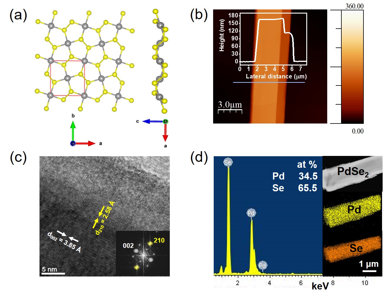
Using the SXRD refinement, the structure of the as-grown crystals was calculated to be orthorhombic (as shown in Figure 1a) with the lattice parameters Å, Å, Å and (point group symmetry ). Layers of PdSe2 are stacked together with an interlayer vdW force along the -axis. The unit cell consists of four Pd atoms and eight Se atoms in a unique puckered pentagonal morphology. Each Pd atom is tetra-coordinated with Se atoms, due to the typical configuration of Pd2+ ions which usually adopts square-planar coordination.
Mechanical exfoliation was performed using a scotch-tape or PDMS to transfer PdSe2 flakes on Si substrate coated with an SiO2 layer of width 285 nm, whereas liquid phase exfoliation was carried out in isopropyl alcohol. The height profile shown in Figure 1b corresponding to the atomic force microscope (AFM) image confirmed the bulk nature of the chosen flakes (thickness 150 nm). FESEM image of a PdSe2 single crystal is shown in Figure S1b. EDS study confirmed the desired stoichiometry of the as-grown crystals (33.24% of Pd and 66.76% of Se). Core level X-ray photoelectron spectra for Pd and Se orbitals are shown in Figure S1c. Pd and peaks are located at 336.1 eV and 341.3 eV, respectively and Se and peaks are located at 54.1 eV and 54.8 eV, respectively which are consistent with the reported binding energies of PdSe2 crystals 34. The lattice planes of PdSe2 crystal were characterized by Transmission Electron Microscope (TEM) as shown in Figure 1c. The d-spacings were calculated to be 3.85 Å and 2.58 Å for planes (002) and (210), respectively which are consistent with that obtained from the crystallographic information file (CIF) extracted from SXRD refinement. Inset of Figure 1c displays the selected area electron diffraction (SAED) pattern where the first order bright spots denote different Bragg planes. The elemental mapping of the exfoliated flake is depicted in Figure 1d which indicates that a slight Se vacancy created at the time of exfoliation (34.5 % of Pd and 65.5 % of Se). Raman spectroscopy for pristine as well as doped samples was carried out for optical characterization which exhibits six vibrational modes (3Ag and 3B1g) including a mixed one (see supplementary for details).
A. Angle-resolved photoemission spectroscopy
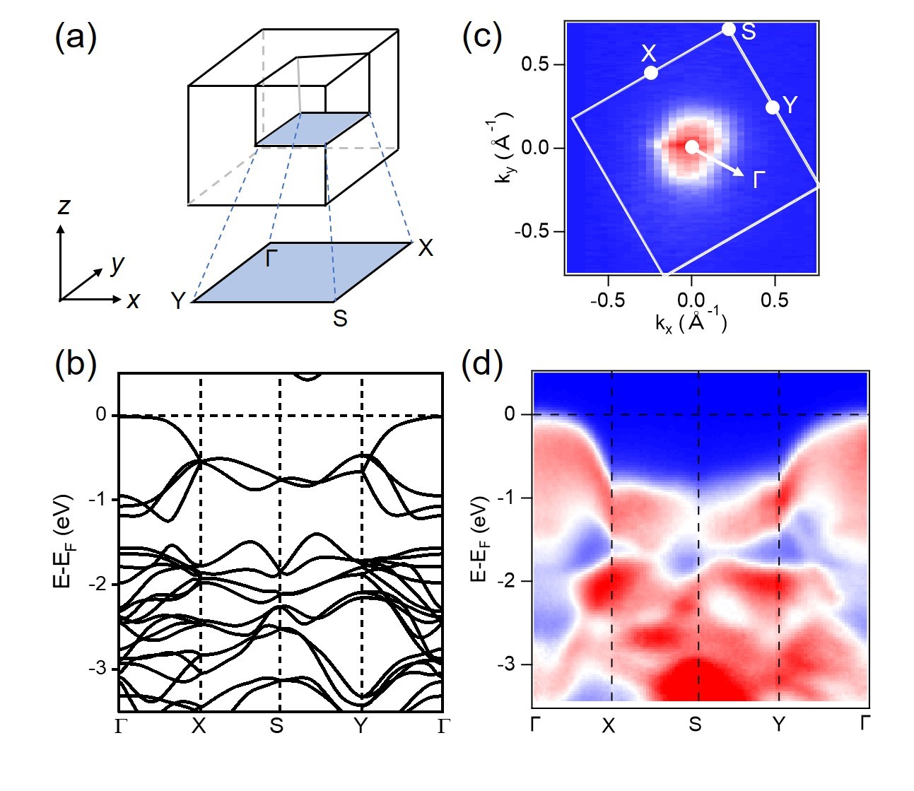
To investigate the electronic structure of pristine bulk PdSe2 crystal and confirm the electronic homogeneity, angle-resolved photoemission spectroscopy (ARPES) experiment were performed with a -focused photon beam. Figure 2b shows the simulated band structure along the high symmetry directions as illustrated in the Brillouin zone of bulk PdSe2 in Figure 2a. As can be seen, the valence band maximum (VBM) is located at the point, whereas, the conduction band minimum (CBM) appears along the SY symmetry direction. The experimental band structure of this material along the high symmetry directions shown in Figure 2d is further corroborated using DFT calculations (see Figure 2b) and previous ARPES reports 35, 36, 37. This also substantiates the single-crystallinity of the grown crystals. Figure 2c shows the Fermi surface map where a weak spectral weight originating from the VBM at is visible without any additional feature originating from the CBM along the SY symmetry direction. This suggests the sample is a p-type semiconductor and the CBM lies above the Fermi level thus inaccessible in ARPES measurement, which is consistent with the previous work 35. In addition, the VBM disperses isotropically, mainly along the X and Y symmetry directions, with almost similar in-plane hole effective masses indicating that the in-plane anisotropy in the electrical transport reported by Pi et al., 38 has other extrinsic origin and anisotropic defects distribution 39 might be an important factor to take into account.
B. Field-effect transistor characteristics
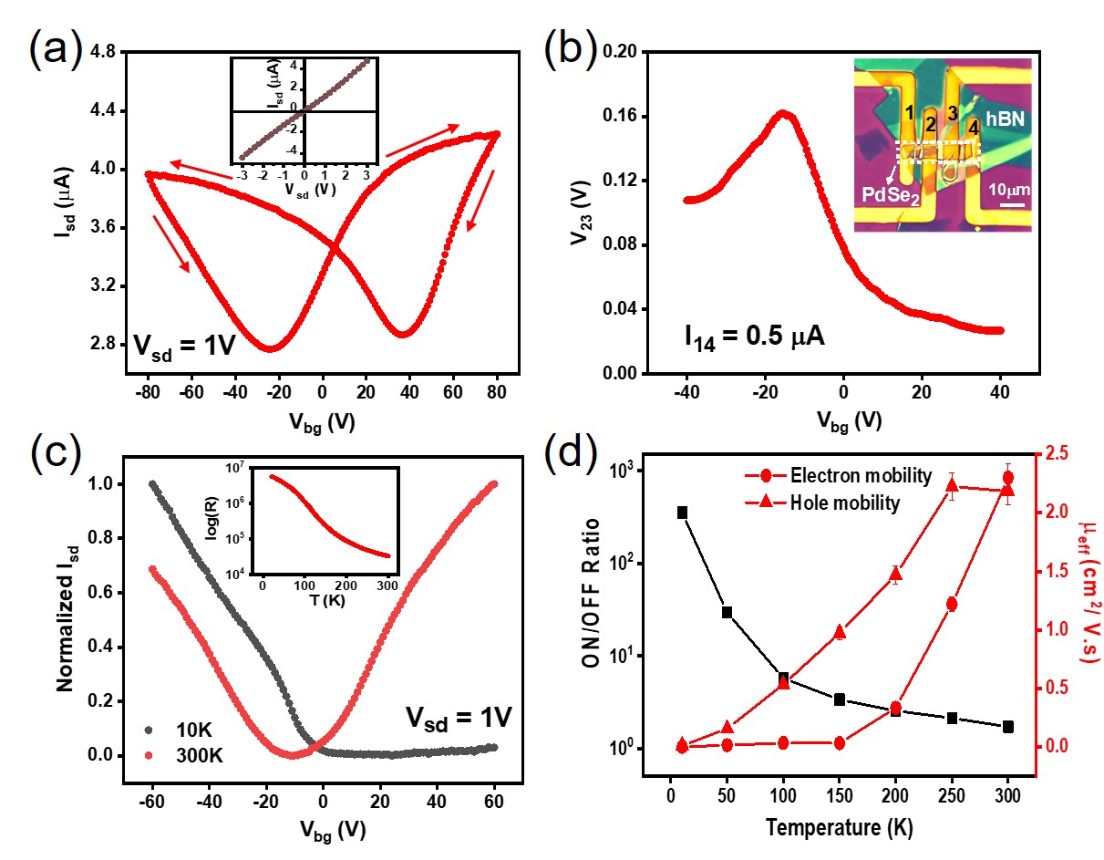
To investigate the electronic transport properties of pristine and doped samples, PdSe2 FET devices were fabricated in both two-probe and four-probe configurations using optical lithography followed by Cr-Au evaporation. The variation of the source-drain current () as a function of back-gate voltage () with 1V bias () in a two-terminal device with PdSe2 flake, shown in Figure 3a, exhibits ambipolar behavior with a slight asymmetry between electrons and holes. The prominence in the n-type characteristics is due to the Se surface vacancies created naturally during the exfoliation from single crystals which causes the excess of electrons in the system. The clockwise hysteresis in curve implies the defect states encountered in the PdSe2 device are static defects 40. Inset of Figure 3a shows the linear variation of drain current (Isd) with source-drain bias voltage (Vsd) at =0 V indicating that a good ohmic type of contact is formed at the metal junction contrary to the conventional TMDCs (e.g. MoS2), thereby reduces the probability of Fermi level pinning effect at the metal-semiconductor junction 41, 42. For the four-probe measurement, the gate-dependence of the voltage between two middle probes with 0.5 A current bias is shown in Figure 3b. Inset of Figure 3b illustrates an optical microscopic image of a four-terminal hBN covered bulk PdSe2 device. Although 90% of the fabricated devices which are exposed in ambient condition show stable ambipolar transfer characteristics with time (more than six months with 1-2% variation in mobility observed in 16 devices), the PdSe2 device (shown in the inset) was protected by a few-layer (thickness 20 nm) hexagonal boron nitride (hBN) to resist any surface contamination, if at all there is any (hBN was used to cover the device from the top of the contacts to avoid the presence of hBN tunnel barrier which can be a major issue for hBN layer under the contacts). A standard schematic of a four-terminal hBN-PdSe2 device in back-gated configuration is depicted in Figure S2a. The two-probe field-effect mobility () was calculated from the linear region of the transfer characteristics using the formula,
| (1) |
where L and W denote the channel length and channel width of the FET device, is the gate capacitance of the SiO2 layer which can be estimated as, , d being the thickness of the SiO2 layer and the corresponding dielectric constant = 3.9. At room temperature the estimated two-probe field-effect mobility () for electrons is slightly greater than that of holes (2.3 cm2/V.s for electrons and 1.6 cm2/V.s for holes) and the transistor ON/OFF ratio is 2. Such a small ON/OFF ratio indicates that bulk PdSe2 exhibits low band gap semiconducting behavior. Room temperature four-probe mobility was estimated from the formula,
| (2) |
where is the voltage between two voltage probes separated by distance D and is the current flowing from terminal-1 to 4. In four-probe configuration the electron mobility was estimated as 21 cm2/V.s and the corresponding hole mobility was 3.4 cm2/V.s.
When the temperature is decreased towards 10 K, the prominence in the n-type behavior is suppressed and the FET characteristics becomes more of p-type with an ON/OFF ratio 100 (Figure S2b). This is expected because at low temperature the thermal energy () is not sufficient to overcome the energy barrier of the Se defects. So the defect states can not take part in conduction. A comparative study of the temperature-dependent transfer characteristics is depicted in Figure 3c. Inset shows the resistance (R) temperature (T) curve in log scale which exhibits a semiconducting nature with a resistance of 30 at room temperature and 5 M at 10 K. Temperature dependence of the two-probe field-effect mobility as well as transistor ON/OFF ratio are shown in Figure 3d which clearly justifies that at room temperature electron mobility is higher than hole mobility and as the temperature decreases hole mobility dominates. The transport band-gap () was extracted from an Arrhenius plot of the minimum source-drain current () temperature (Figure S2c) by using the formula 43,
| (3) |
where is the Boltzmann constant. The extracted value of the band-gap is 0.09 eV. The existence of trap-states usually underestimates the band-gap calculated from this method.
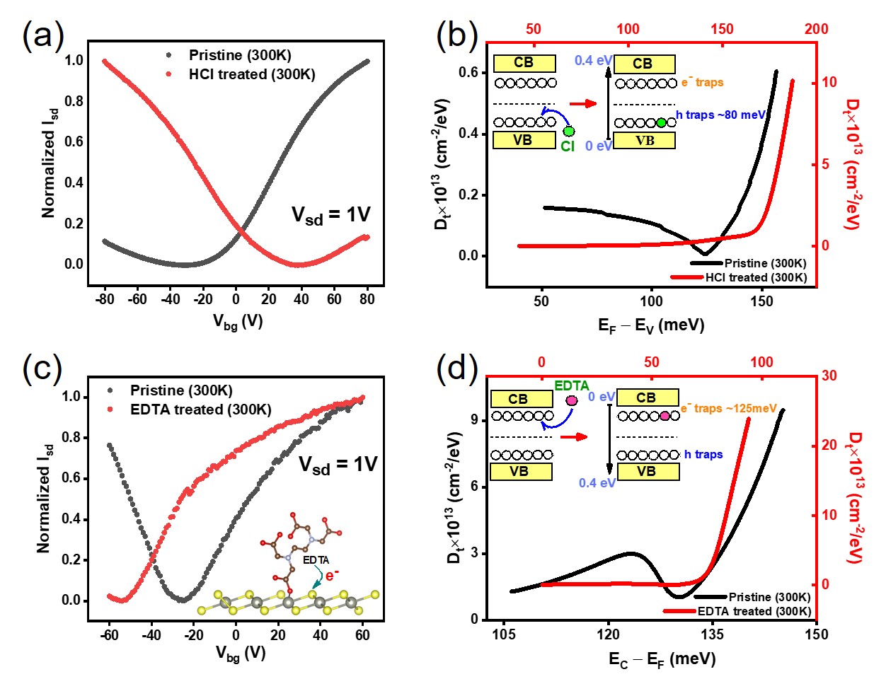
After dipping in the HCl solution, the threshold voltage shifts from -20V to 40V towards positive gate bias and the behavior of the PdSe2 transistor turns out to be more of p-type (Figure 4a) with the hole mobility increased to 5 cm2/V.s. It is predicted that the un-ionized Cl when chemically adsorbed on surface vacancy sites, draws the electrons from the system because of its high electron affinity and thereby, increases the hole carrier injection. At low temperature, the electron transport is almost negligible and the threshold point gets a huge positive shift as shown in Figure S3a. ON/OFF ratio and field-effect hole mobility as a function of temperature for an HCl treated device are depicted in Figure S3b.
On the other hand, EDTA4- ion acts as a strong electron donor and usually forms metal complexes via four carboxylate and two amine groups in aqueous solution. EDTA is attached by the COO- bond with the Pd atoms around the Se vacancy sites. As an electron donor EDTA repairs the Se vacancies and corresponds to a much prominent n-type character with a more negative shift of threshold point (from -25V to -54V) as shown in Figure 4c. At low temperature contribution from the defect states is negligible, thereby hole transport gets enhanced (Figure S3c). The ON/OFF ratio and field-effect mobilities as a function of temperature for an EDTA treated device are depicted in Figure S3d.
EDTA and HCl treated devices were observed with time to check their stability. Notably, the behavior of EDTA doped PdSe2 FET has no such significant change with time as shown in Figure S4a. In case of HCl treated device, the threshold gate voltage suffers a backward shift (from 40V to 20V) with time as shown in Figure S4b and the change in hole mobility is around 5-8%. This nominal change may be a consequence of the air-exposure effect.
C. Density of defect states
The hysteresis observed in the gate-dependent transfer characteristics as shown in Figure 3a corresponds to the trapped charges encountered by the defect states in the device 44, 45, 46. A simple correlation between the width of the hysteresis and the density of the defect states can be illustrated by differentiating the trapped charge concentration () with respect to the corresponding Fermi level 47. can be calculated from the formula : = , where is basically the width of the hysteresis. Density of defect states () can now be estimated from (see supplementary for detail calculation). Figure 4b represents the density of defect states at 300 K of the pristine as well as HCl doped device towards the valence band side. Likewise, Figure 4d represents the same for pristine as well as EDTA doped device towards the conduction band side. Chlorine draws the electrons from the system and injects holes, thus reduces the defect-induced electron conduction. The injected hole carriers fill the empty shallow traps near the valence band side ( 50-100 meV from valence band edge) and acts as an acceptor level for p-type conduction resulting in a decrease in the density of defect states in the vicinity of valence band edge (Inset shows the schematic of repairing the defect states by Cl treatment taking 80 meV as a reference energy point of trap states). In a similar manner, when the device is processed through EDTA treatment, EDTA donates excess electrons in the channel and the electron traps within the band gap ( 125 meV from conduction band edge) get filled resulting in the enhancement of electron transport (Inset shows the schematic of repairing the defect states by EDTA treatment taking 125 meV as a reference energy point of trap states). This justifies that Cl or EDTA repairs the Se vacancies and thereby causes a decrease in the number of defect states (here the band gap of pristine device is considered to be 0.4 eV as estimated from DFT calculation).
D. Density functional theory
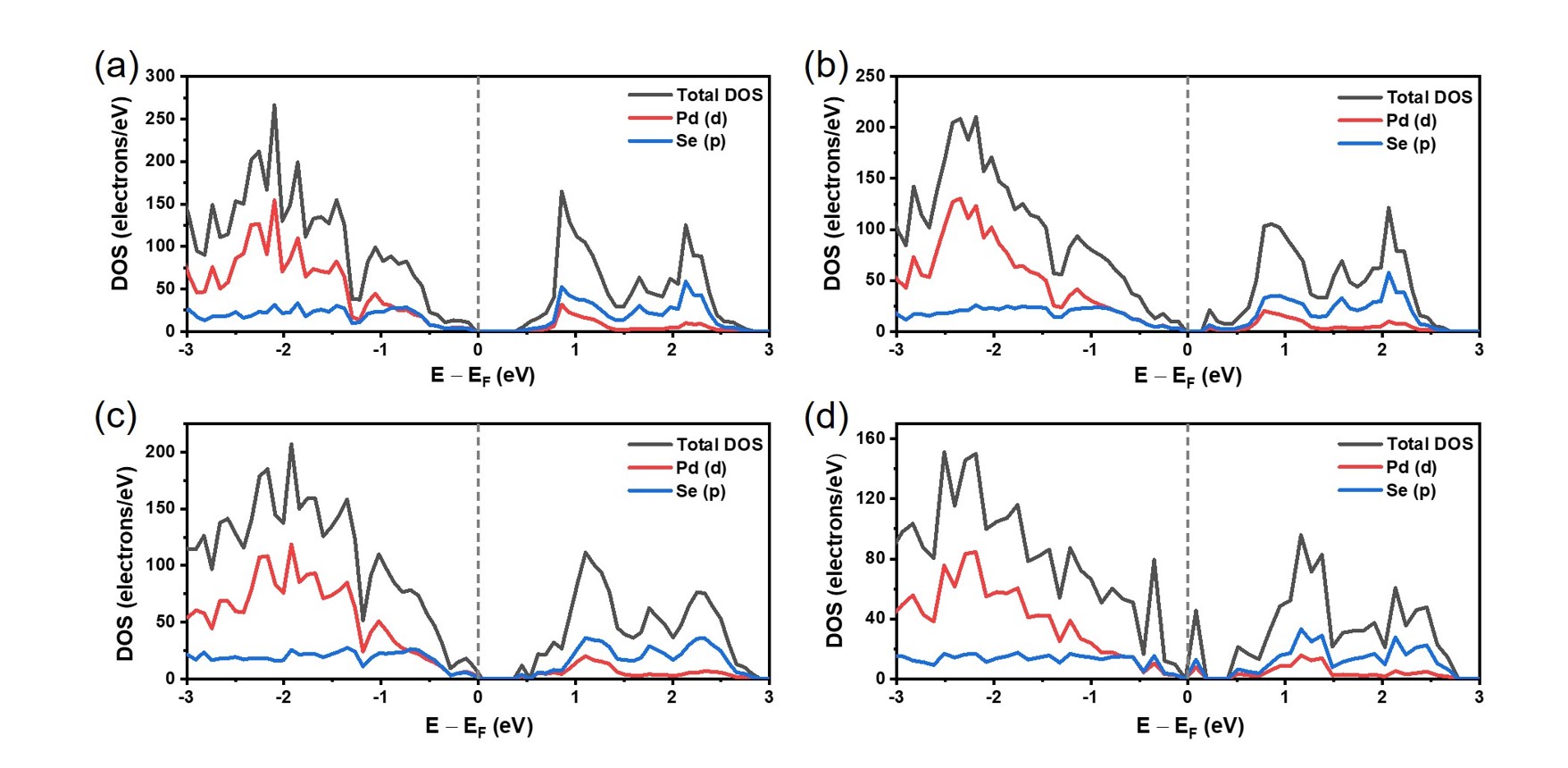
The simulated structure parameters of the fully relaxed geometry obtained from Density functional theory calculation are Å, Å, Å, which shows a good agreement with the experimental parameters obtained from single crystal XRD 48. The electronic band structure shown in Figure 2b of pristine bulk PdSe2 exhibits a 0.4 eV indirect band gap. According to the calculated density of states (Figure 5a), there is a transition from Pd states (valence band side) to Se states (conduction band side) which indicates that charge transfer occurs from Pd to Se. This was also verified by bader charge analysis using VASP which shows 0.03e amount of charge is transferred from Pd to each Se. Phonon modes are simulated for pristine sample depicted elaborately in supplementary. Figure 5b displays the in-gap states arise closed to the conduction band when Se surface vacancies are imported and thereby causes a certain decrease in the band gap (0.16 eV). The defect state thus generated corroborates with the slight dominance in electron conduction at room temperature. Cl-doping at the Se vacancy sites repairs the gap-states and modifies the density of states as shown in Figure 5c which implies a shifting of Fermi level towards valence band and thereby amplifies the p-type character as obtained from FET measurement. On the other hand, after the adsorption of EDTA molecule some impurity states arise between the Fermi level and conduction band edge (Figure 5d) which well agrees with the electron-enhanced transport in EDTA-treated PdSe2 channel.
5 Conclusions
In summary, PdSe2 single crystals are synthesized successfully with desirable stoichiometry. The ambipolar behaviour of PdSe2 microelectronic devices with low ON/OFF ratio offers moderate electron mobility that may be enhanced in its monolayer analogue. Also, we demonstrate the tunability in the electronic transport properties of bulk PdSe2 layer as a result of chemical doping. The dominance of the electron-transport in the pristine device is arrested when the device is processed by HCl. On the other hand, EDTA/Na2 salt solution acts as an n-type dopant and almost suppresses the hole-transport. The phonon modes for pristine, as well as doped samples, are identified using Raman spectroscopy experiment. The effect of vacancy defects as well as chemical doping, as observed in the transfer charateristics, are also supported by the first principle DFT calculations. A simplified analytic approach is considered to calculate the density of defect states which also clarifies that Cl and EDTA occupy the hole traps and electron traps, respectively, and resulting in a decrease of the number of defect states. In addition, temperature dependent electronic properties of PdSe2 depicts the change of the nearly symmetrical ambipolar characteristics at room temperature to almost p-type behavior at low temperature which is also confirmed by the low temperature -ARPES spectra. Our results illustrate that PdSe2 can be a promising candidate in fabricating single transistor logic gates in the form of dual-gated complementary metal-oxide-semiconductor (CMOS). Also, the tunable ambipolarity would be beneficial in the field of hyperscaling and multivalued logic circuitry.
6 Acknowledgments
The financial supports from IACS, DST-INSPIRE and CSIR-UGC are greatly acknowledged. TK would like to thank Prof. Debashree Ghosh along with her lab members, Mr. Sudipta Biswas and Mr. Soumya Mondal for computational help. TK appreciates Mr. Satyabrata Bera, Mr. Soumik Das, Mr. Sourav Mondal, Mr. Sanjib Naskar and Ms. Anwesha Datta for the experimental support. She also acknowledges the furnace facility of Dr. Mintu Mondal, procured under DST-SERB grant No. SRG/2019/000674. TK is also thankful to IACS cluster facility for the computational study reported in this paper. SD acknowledges the financial support from DST-SERB grant No. CRG/2021/004334. SD also acknowledges support (lithography facility) from the Technical Research Centre (TRC), IACS, Kolkata. The research leading to micro-ARPES results in Elettra under Proposal No. 20220474 has been supported by a grant from the Italian Ministry of Foreign Affairs and International Cooperation and the Indian Department of Science & Technology.
S.D., and T.K. conceived the project and designed the experiments. T.K., B.D., and R.P. prepared the samples and performed their initial characterization together with S.M. M.P., S.M., and T.K. carried out the device fabrication and modification. T.K., and B.D. performed the electrical measurements and analyzed the data. S.D., and B.P. developed the analytical model, with contributions from B.D. S.K.M., B.D. and S.D. conceived the ARPES measurements. M.K., and A.B. provided the technical help during the beamtime. All DFT calculations were performed by T.K. with the close discussions with S.D. All authors discussed the results and actively commented on the manuscript written by T. K. and S.D. with the the input from S.K.M.
References
- 1 Zhao, W.; Ghorannevis, Z.; Chu, L.; Toh, M.; Kloc, C.; Tan, P.-H.; Eda, G. Evolution of Electronic Structure in Atomically Thin Sheets of WS2 and WSe2. ACS Nano 2013, 7(1), 791–797.
- 2 Radisavljevic, B.; Radenovic, A.; Brivio, J.; Giacometti, V.; Kis, A. Single-layer MoS2 transistors. Nat. Nanotech. 2011, 6(3), 147-150.
- 3 Kong, D.; Wang, H.; Cha, J. J.; Pasta, M.; Koski, K. J.; Yao, J.; Cui, Y. Synthesis of MoS2 and MoSe2 Films with Vertically Aligned Layers. Nano Lett. 2013, 13(3), 1341-1347.
- 4 D. Hu, G. Xu, L. Xing, X. Yan, J. Wang, J. Zheng, Z. Lu, P. Wang, X. Pan, L. Jiao, Angew. Two-Dimensional Semiconductors Grown by Chemical Vapor Transport. Chem. Int. Ed. 2017, 56, 3611.
- 5 Xinsheng Wang, Hongbin Feng, Yongmin Wu, and Liying Jiao. Controlled Synthesis of Highly Crystalline MoS2 Flakes by Chemical Vapor Deposition. J. Am. Chem. Soc. 2013, 135(14), 5304–5307.
- 6 Yankowitz, M., Ma, Q., Jarillo-Herrero, P. . van der Waals heterostructures combining graphene and hexagonal boron nitride. Nat Rev Phys 2019, 1, 112–125.
- 7 Debora Pierucci, Hugo Henck, Jose Avila, Adrian Balan, Carl H. Naylor, Gilles Patriarche, Yannick J. Dappe, Mathieu G. Silly, Fausto Sirotti, A. T. Charlie Johnson . Band Alignment and Minigaps in Monolayer MoS2-Graphene van der Waals Heterostructures. Nano Lett. 2016, 16(7), 4054–4061.
- 8 Hyo-Jik Nam, Jinok Kim, and Jin-Hong Park. Wide-Range Controllable Doping of Tungsten Diselenide (WSe2) based on Hydrochloric Acid Treatment. J. Phys. Chem. C 2017, 121(26), 14367–14372.
- 9 Hau-Vei Han, Ang-Yu Lu, Li-Syuan Lu, Jing-Kai Huang, Henan Li, Chang-Lung Hsu, Yung-Chang Lin, Ming-Hui Chiu, Kazu Suenaga, Chih-Wei Chu . Photoluminescence Enhancement and Structure Repairing of Monolayer MoSe2 by Hydrohalic Acid Treatment. ACS Nano 2015, 10(1), 1454–1461.
- 10 Meng, Y., Ling, C., Xin, R. . Repairing atomic vacancies in single-layer MoSe2 field-effect transistor and its defect dynamics. npj Quant Mater 2017, 2, 16.
- 11 Pi, L. J., Li, L., Liu, K. L., Zhang, Q. F., Li, H. Q., Zhai, T. Y. Recent Progress on 2D Noble-Transition-Metal Dichalcogenides. Adv. Funct. Mater. 2019, 29, 1904932.
- 12 Y. Wang, L. Li, W. Yao . Monolayer PtSe2, a New Semiconducting Transition-Metal-Dichalcogenide, Epitaxially Grown by Direct Selenization of Pt. Nano Lett. 2015, 15(6), 4013–4018.
- 13 A. Oyedele, S. Yang, L. Liang . PdSe2: Pentagonal Two-Dimensional Layers with High Air Stability for Electronics. J. Am. Chem. Soc. 2017, 139(40), 14090–14097.
- 14 Zhao, Y., Qiao, J., Yu, P., Hu, Z., Lin, Z., Lau, S.P., Liu, Z., Ji, W. and Chai, Y. Extraordinarily Strong Interlayer Interaction in 2D Layered PtS2. Adv. Mater. 2016, 28, 2399-2407.
- 15 Y. Zhao, J. Qiao, Z. Yu, P. Yu, K. Xu, S. P. Lau, W. Zhou, Z. Liu, X. Wang, W. Ji, Y. Chai. High-Electron-Mobility and Air-Stable 2D Layered PtSe2 FETs. Adv. Mater. 2017, 29, 1604230.
- 16 Artem V. Kuklin, Lyudmila V. Begunovich, Lingfeng Gao, Han Zhang, and Hans Ågren. Point and complex defects in monolayer PdSe2: Evolution of electronic structure and emergence of magnetism. Phys. Rev. B 2021, 104, 134109.
- 17 Hoffman, A.N., Gu, Y., Liang, L. . Exploring the air stability of PdSe2 via electrical transport measurements and defect calculations. npj 2D Mater Appl, 2019, 3, 50.
- 18 Chow, W. L., Yu, P., Liu, F., Hong, J., Wang, X., Zeng, Q., Hsu, C.-H., Zhu, C., Zhou, J., Wang, X. . High Mobility 2D Palladium Diselenide Field-Effect Transistors with Tunable Ambipolar Characteristics. Adv. Mater. 2017, 29, 1602969.
- 19 Li, J., Joseph, T., Ghorbani-Asl, M., Kolekar, S., Krasheninnikov, A. V., Batzill, M.. Edge and Point-Defect Induced Electronic and Magnetic Properties in Monolayer PtSe2. Adv. Funct. Mater. 2022, 32, 2110428.
- 20 Xueyuan Liu, Bing Sun, Kailiang Huang, Chao Feng, Xiao Li, Zhen Zhang, Wenke Wang, Xin’gang Zhang, Zhi Huang, Huaping Liu . Use of Ambipolar Dual-Gate Carbon Nanotube Field-Effect Transistor to Configure Exclusive-OR Gate. ACS Omega, 2022, 7(10), 8819–8823.
- 21 G. D. Nguyen, L. Liang, Q. Zou, M. Fu, A. D. Oyedele, B. G. Sumpter, Z. Liu, Z. Gai, K. Xiao, A. P. Li. 3D Imaging and Manipulation of Subsurface Selenium Vacancies in PdSe2. Phys. Rev. Lett. 2018, 121, 086101.
- 22 H. P. Komsa, S. Kurasch, O. Lehtinen, U. Kaiser, A. V. Krasheninnikov. From point to extended defects in two-dimensional MoS2: Evolution of atomic structure under electron irradiation.Phys. Rev. B, 2013, 88, 035301.
- 23 Zhao, X.W., Yang, Z., Guo, J.T. . Tuning electronic and optical properties of monolayer PdSe2 by introducing defects: first-principles calculations. Sci Rep 2020, 10, 4028.
- 24 Ghazanfar Nazir, Muhammad Farooq Khan, Volodymyr M. Iermolenkoa and Jonghwa Eom. Two- and four-probe field-effect and Hall mobilities in transition metal dichalcogenide field-effect transistors. RSC Adv. 2016, 6, 60787-60793.
- 25 P. Dudin, P. Lacovig, C. Fava, E. Nicolini, A. Bianco, G. Cautero, A. Barinov and J. Synchrotron Radiat. Angle-resolved photoemission spectroscopy and imaging with a submicrometre probe at the SPECTROMICROSCOPY-3.2L beamline of Elettra. J. Synchrotron Rad. 2010, 17, 445–450.
- 26 G. Kresse, J. Furthmüller. Efficiency of ab-initio total energy calculations for metals and semiconductors using a plane-wave basis set. Comp. Mater. Sci. 1996, 6, 15-50.
- 27 G. Kresse, J. Furthmüller. Efficient iterative schemes for ab initio total-energy calculations using a plane-wave basis set. Phys. Rev. B 1996, 54, 11169-11186.
- 28 Perdew, J. P.; Burke, K.; Ernzerhof, M. Generalized Gradient Approximation Made Simple. Phys. Rev. Lett. 1996, 77(18), 3865.
- 29 H.J. Monkhorst, J.D. Pack. Special points for Brillouin-zone integrations. Phys. Rev. B 1976, 13, 5188-5192.
- 30 Atsushi Togo and Isao Tanaka. First principles phonon calculations in materials science. Scr. Mater. 2015, 108, 1-5.
- 31 P. Giannozzi . QUANTUM ESPRESSO: a modular and open-source software project for quantum simulations of materials. J. Phys.: Condens. Matter 2009, 21(39), 395502.
- 32 P. Giannozzi . Advanced capabilities for materials modelling with Quantum ESPRESSO. J. Phys.: Condens. Matter 2017, 29(46), 465901.
- 33 K. Momma and F. Izumi. VESTA 3 for three-dimensional visualization of crystal, volumetric and morphology data. J. Appl. Crystallogr. 2011, 44, 1272-1276.
- 34 Nishiyama, W., Nishimura, T., Ueno, K., Taniguchi, T., Watanabe, K., Nagashio, K., Quantitative Determination of Contradictory Bandgap Values of Bulk PdSe2 from Electrical Transport Properties. Adv. Funct. Mater. 2022, 32, 2108061.
- 35 C. Gu, ., Low-lying electronic states with giant linear dichroic ratio observed in PdSe2. Phys. Rev. B 2022, 106, L121110.
- 36 M. Cattelan ., Site-specific symmetry sensitivity of angle-resolved photoemission spectroscopy in layered palladium diselenide. 2D Mater. 2021, 8, 045036.
- 37 J. H. Ryu ., Direct Observation of Orbital Driven Strong Interlayer Coupling in Puckered Two-Dimensional PdSe2. Small 2022, 18, 2106053.
- 38 L. Pi ., Highly In-Plane Anisotropic 2D PdSe2 for Polarized Photodetection with Orientation Selectivity. Adv. Funct. Mater. 2021, 31, 2006774.
- 39 X. Liu ., Temperature-sensitive spatial distribution of defects in PdSe2 flakes. Phys. Rev. Mater. 2021, 5, L041001.
- 40 Kaushik, N., Mackenzie, D.M.A., Thakar, K. et al. Reversible hysteresis inversion in MoS2 field effect transistors. npj 2D Mater Appl 2017, 1, 34.
- 41 F. Giannazzo, G. Fisichella, A. Piazza, S. Agnello, and F. Roccaforte. Nanoscale inhomogeneity of the Schottky barrier and resistivity in MoS2 multilayers. Phys. Rev. B 2015, 92, 081307.
- 42 Pantelis Bampoulis, Rik van Bremen, Qirong Yao, Bene Poelsema, Harold J. W. Zandvliet, and Kai Sotthewes. Defect Dominated Charge Transport and Fermi Level Pinning in MoS2/Metal Contacts. ACS Appl. Mater. Interfaces 2017, 9(22), 19278–19286.
- 43 George Zhang, Matin Amani, Apoorva Chaturvedi . Optical and electrical properties of two-dimensional palladium diselenide. Appl. Phys. Lett. 2019, 114, 253102.
- 44 H.-C. Lin, C.-H. Hung, W.-C. Chen, Z.-M. Lin, H.-H. Hsu, and T.-Y. Hunag. Origin of hysteresis in current-voltage characteristics of polycrystalline silicon thin-film transistors. J. Appl. Phys. 2009, 105(5), 054502.
- 45 T. Li, G. Du, B. Zhang, and Z. Zeng. Thermally activated trap charges responsible for hysteresis in multilayer MoS2 field-effect transistors. Appl. Phys. Lett. 2014, 105(5), 093107.
- 46 P. Joshi, H. E. Romero, A. T. Neal, V. K. Toutam, and S. A. Tadigadapa. Intrinsic doping and gate hysteresis in graphene field effect devices fabricated on SiO2 substrates. Journal of Physics. Condensed matter: An Institute of Physics Journal 2010, 22(33), 334214.
- 47 Qiang Xu, Yingri Sun, Peng Yang, . Density of defect states retrieved from the hysteretic gate transfer characteristics of monolayer MoS2 field effect transistors. AIP Advances 2019, 9, 015230.
- 48 Soulard, C.; Rocquefelte, X.; Petit, P.-E.; Evain, M.; Jobic, S.; Itie, J.-P.; Munsch, P.; Koo, H.-J.; Whangbo, M.-H. Experimental and theoretical investigation on the relative stability of the and pyrite-type structures of PdSe2. Inorg. Chem. 2004, 43(6), 1943-1949.