supp
Extended-SWIR GeSn LEDs with reduced footprint and power consumption
Abstract
†These authors contributed equally to this work.
Abstract
CMOS-compatible short- and mid-wave infrared emitters are highly coveted for the monolithic integration of silicon-based photonic and electronic integrated circuits to serve a myriad of applications in sensing and communications. In this regard, a group IV germanium-tin (GeSn) material epitaxially grown on silicon (Si) emerges as a promising platform to implement tunable infrared light emitters. Indeed, upon increasing the Sn content, the bandgap of GeSn narrows and becomes direct, making this material system suitable for developing an efficient silicon-compatible emitter. With this perspective, microbridge PIN GeSn LEDs with a small footprint of m2 are demonstrated and their operation performance is investigated. The spectral analysis of the electroluminescence emission exhibits a peak at m and it red-shifts slightly as the driving current increases. It is found that the microbridge LED operates at a dissipated power as low as W at room temperature and just W at K. This demonstrated low operation power is comparable to that reported for LEDs having a significantly larger footprint reaching m2. The efficient thermal dissipation of the current design helped to reduce the heat-induced optical losses, thus enhancing light emission. Further performance improvements are envisioned through thermal and optical simulations of the microbridge design. The use of GeSnOI substrate for developing a similar device is expected to improve optical confinement for the realization of electrically driven GeSn lasers.
Reducing the footprint of CMOS-compatible optical interconnects is a key paradigm to address the relentless course toward the very dense integration of chips while maintaining high bandwidth and low power consumption Soref2014 ; Saito2014 ; Deen2012 . In fact, as future electronic chips require further device scaling, the associated miniaturization of metal interconnects suffers fundamental limits leading to high impedance and joule heating, which consequently limits the bandwidth. This stimulates a remarkable interest in merging silicon photonics with silicon-based integrated circuits for more efficient inter-chip and intra-chip communication, besides added multifunctional abilities such as on-chip optical modulation, spectroscopy, and sensing applications Soref2006 . However, the development of CMOS-compatible on-chip light sources remains a huge challenge owing to the lack of direct bandgap group IV semiconductors Liang2010 ; Zhou2015 . Recently, GeSn has become a promising solution to overcome this limitation since GeSn becomes a direct bandgap material when sufficient Sn content is incorporated in Ge lattice Moutanabbir2021 ; VondenDriesch2015 . Indeed, the indirect-direct bandgap crossover occurs at a Sn content of around at. % in relaxed GeSn. Increasing the Sn content beyond this threshold improves the bandgap directness and lowers its energy, enhancing the light emission efficiency wirths2015lasing . Photodetector devices made of chemical vapor deposition (CVD) and molecular beam epitaxy (MBE) grown layers and heterostructures have been demonstrated to operate at wavelengths up to m in the mid-infrared (MIR) spectral range Atalla2021 . While optically pumped GeSn-based lasers have been reported by many researchers recently Moutanabbir2022 , experimental attempts to develop the electrically injected counterparts remain relatively scarce Buca2022 ; Marzban2022 .
To achieve the dense integration of Si-based integrated circuits and silicon photonics, emitters with a small footprint and reduced power consumption are strongly desired. Several efforts have been expended toward this goal Oehme2011 ; Tseng2013 ; Gupta2013 ; Gallagher2015 ; Stange2017 ; Peng2020 . While early GeSn LEDs feature low power consumption of 3.75 W, these devices have a remarkably large footprint area of around m2 Gupta2013 . Other LED devices reported later on had two orders of magnitude smaller device sizes of around m2, but they require more than -fold higher power consumption Huang2019 . Herein, we present a GeSn microscale LED with a record-small footprint of around m2 yet operating at a low dissipated power around W at K and around W at room temperature. This is realized through a cavity LED utilized in a microbridge structure.
I Results and discussion
Growth and characterization of GeSn epilayers and LED fabrication.
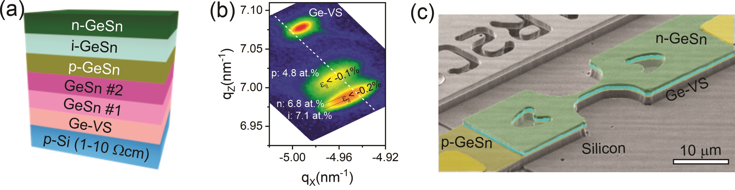
The GeSn LED samples were grown using a low-pressure CVD reactor following a multilayer growth to control lattice strain and Sn content, as schematically illustrated in Fig. 1(a). Starting from a -inch Si (100) wafer, a m thick Ge virtual substrate (VS) was grown using % monogermane (GeH4) and a constant ultrapure H2 flow implementing a two-temperature growth process at and ∘C, followed by thermal cyclic annealing above ∘C. Two GeSn buffer layers, with thicknesses of and nm, were grown using GeH4 and tin-tetrachloride (SnCl4) precursors at initial molar fractions of ( ) and ( ), respectively. The second GeSn buffer layer was grown at a low temperature allowing more Sn to be substitutionally incorporated into the Ge lattice. Then, PIN GeSn layers were grown at thicknesses of , , and nm, respectively. The p- and n-type doping were achieved using diborane (B2H6) and arsine (AsH3) precursors, respectively. According to the X-ray diffraction (XRD) reciprocal space mapping (RSM) measured around the asymmetrical (224) reflection peak, as shown in Fig. 1(b), the Sn content is estimated to be at. % (#1), at. % (#2), at. % (p-GeSn), at. % (i-GeSn), at. % (n-GeSn), respectively. It is also noticeable that the layers are remarkably relaxed with the highest bi-axial compressive strain below % in the i- and n-GeSn layers.
Figure 1(c) displays a scanning electron microscope (SEM) image depicting the fabricated microbridge PIN GeSn LED device. The fabricated device has a microbridge structure for the diodes with a corner-cube cavity which was intended to enhance the light emission via optical confinement armand2019lasing . The microbridge structure with corner-cube mirrors were patterned using photolithography, and the defined pattern was transferred onto the GeSn and Ge VS layers using reactive ion etching (RIE) with Cl2 chemistry. A second photolithography step was performed to anisotropically etch down to expose the p-doped GeSn layer at one end of the device. Thus, the device had exposed p- and n-doped GeSn areas on both ends of the microbridge structure. The patterns for the metal contacts were then defined using photolithography at the p- and n-doped GeSn areas. Subsequently, the Cr and Au contacts with thicknesses of nm and nm, respectively, were deposited as p- and n-layers using electron beam evaporation, followed by the lift-off process.
GeSn PIN LED characterization and performance comparison.
The microbridge device characterization started by measuring the I-V curves using a source meter unit over a wide bias range of up to V in the forward and reverse biases as shown in Fig. 2(a). The LED operates under forward bias reaching up to mA at V, which corresponds to a power consumption as low as W at such relatively high operation bias. The large current under the reverse bias, however, indicates carrier leakage through the depletion region of the device possibly owing to various mechanisms including SRH, tunnel assisted, and diffusion leakages Son2020 ; Dong2017 ; Atalla2023 .
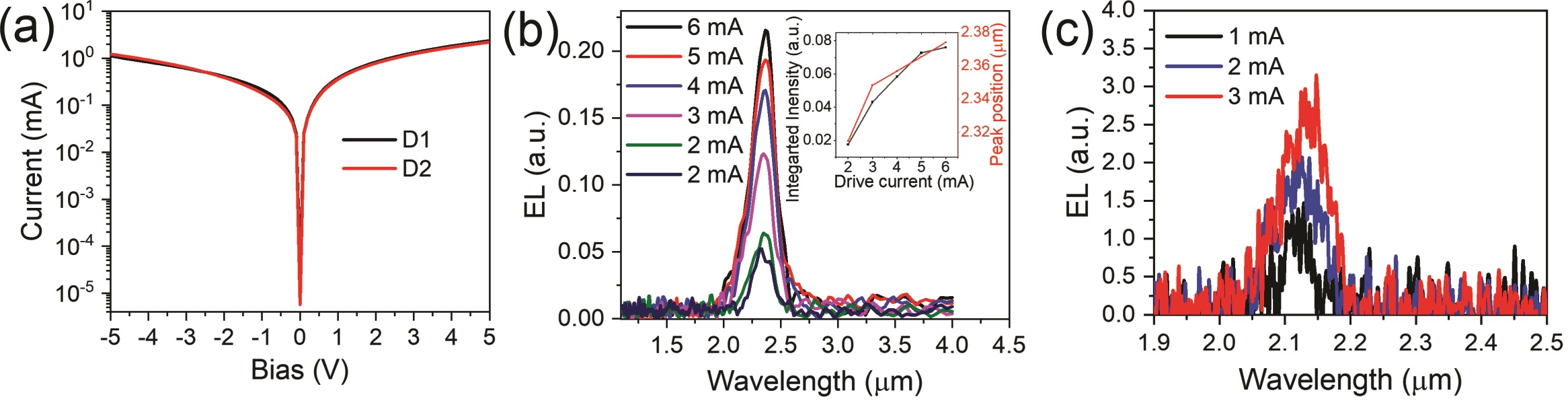
To measure and analyze the LED light emission, a Fourier transform infrared spectroscopy (FTIR) setup was utilised to measure the spectral emission from the microbridge devices. The setup mainly consists of a Bruker FTIR spectrometer, InSb liquid nitrogen cooled photodetector (PD), reflective objective lens, and a translation stage. To amplify the InSb PD signal, it was fed into a current preamplifier and a lock-in amplifier. The signal was re-entered into the FTIR for data processing. The lock-in technique requires the LED light to take the form of pulses either by mounting a mechanical chopper in the light path or by applying AC drive current to the LED. As shown in Fig. 2(b), the electroluminescence (EL) was measured at a driving current from mA to mA with mA stepwise. It is evident that the LED emission peak is centered around m at the lowest drive current, and it red-shifts as the drive current increases, as shown in the inset of Fig. 2(b). The inset also depicts that the integrated intensity of the EL emission initially increases linearly as the driving current increases, while it saturates at V, indicating the drop in the LED emission efficiency possibly due to the heating effect.
The device was also characterized at a cryogenic temperature of K, showing that a clear signal can be measured at a driving current as low as mA. Figure 2(c) shows the EL emission spectra measured at K. It is also clear that the EL peak blue-shifts to m at K compared to a significantly longer wavelength of m measured at room temperature, which is attributed to the increased bandgap at a lower temperature.
Table 1 compares the GeSn LEDs reported until today with a focus on comparing the dissipated power and the device footprint. The table clearly shows that our microbridge LED devices have the lowest combined footprint (m2) and power dissipation (IV) at room temperature and K.
![[Uncaptioned image]](/html/2302.06011/assets/Fig4.jpg)
Corner-cube cavity light confinement effects for improving LED emission and gain properties
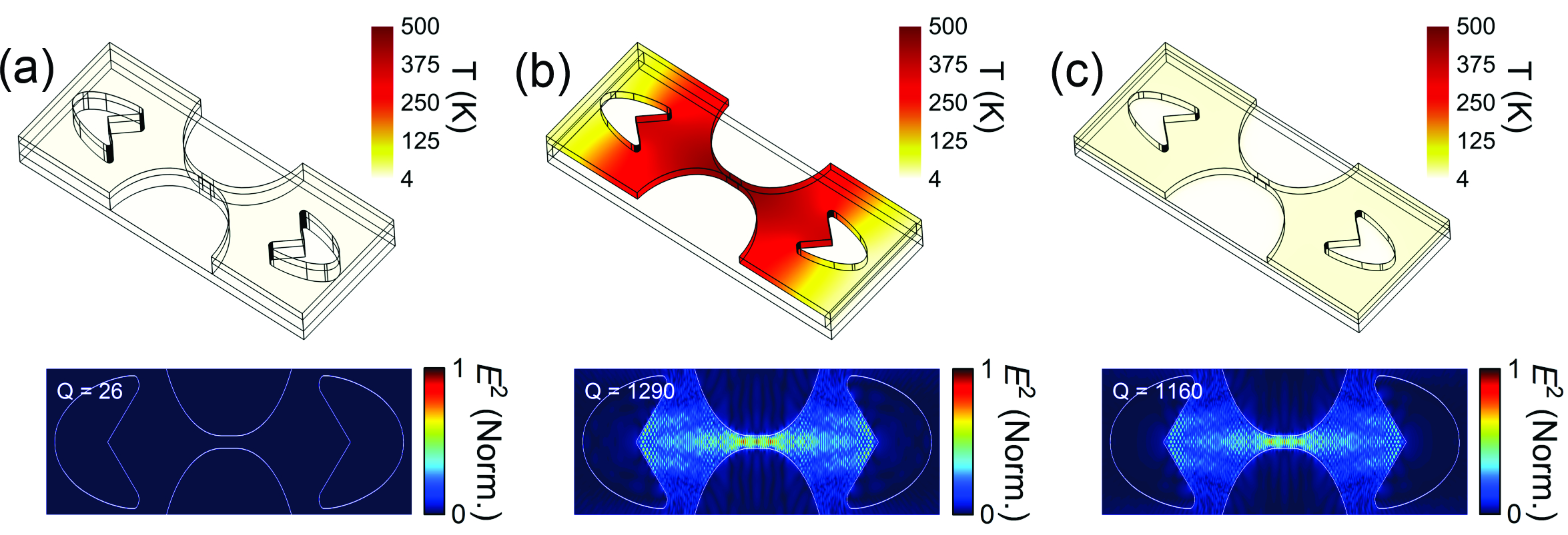
To investigate why the cavity effect is not achieved in our LEDs and provide a viable pathway towards achieving cavity effects and possibly lasing, we performed thermal and optical simulations for the LED structures. Figure 3 presents simulated thermal (top) and optical fields (bottom) distributions calculated using a finite-element method (FEM) and finite-difference time-domain (FDTD), respectively, for three different LED structures. The three structures mimicked the structure used in our experiments and they consisted of: (i) the current device with no under etch (Fig. 3(a)), (ii) suspended structure with Ge VS layer under-etched except at the two ends of the device (Fig. 3(b)), and (iii) ideal fully released GeSn layer (Fig. 3(c)), which is possible by utilizing a GeSn-on-insulator (GeSnOI) structure Burt2021 ; Joo2021 . In the thermal simulation, a heat source with a current density of Acm2 was applied along the current path. The optical field distributions for the three structures were calculated at nm in the optical simulation. All the simulations were conducted at K. As shown in Fig. 3(a), the LED used in our experiments shows superior thermal conduction with a slightly increased temperature of K but it has poor optical confinement with a very low Q factor of due to the significant leakage of optical fields from the GeSn active layer to the Ge VS layer underneath. This explains why the cavity effect is not observed during our experiments. To address the limited optical confinement, we designed and investigated a structure suspended in the air that can be fabricated by etching the Ge VS layer Gupta2013b . In stark contrast to poor optical confinement in the structure used in our experiments, a suspended structure, as shown in Fig. 3(b), shows strong optical confinement with a high Q factor of because large refractive index difference between the GeSn active layer and air prevents the leakage of optical fields. The temperature of an active area, however, is increased significantly to K upon the current injection due to poor thermal dissipation in the suspended device geometry. As the increased temperature hinders optical emission in the active area due to heat-induced optical loss and also due to the reduced optical gain at an elevated temperature Kim2022 , an optimized structure was envisioned to achieve both good optical confinement and thermal dissipation. Fig. 3(c) presents an optimized structure in which a GeSn active layer is laid down onto a SiO2 substrate. It is worth mentioning that the optimized structure can be fabricated using the GeSnOI substrate, which has recently been successfully demonstrated by several research groups Moutanabbir2022 ; Burt2021 ; Joo2021 ; Wang2021 . The optimized structure shows the simultaneous achievement of good heat dissipation with slightly increased temperature of K and superior optical confinement with a high Q factor of . We believe that it is feasible to achieve lasing in the optimized structure.
II Conclusion
In summary, microbridge PIN GeSn LEDs were demonstrated and their operation performance was assessed using electrical and optical characterizations. It was found that the microbridge LED has power dissipation as low as W and a small footprint of m2. The efficient thermal dissipation of the current design helped reduce the heat-induced optical losses and thus enhanced light emission. According to thermal and optical simulations, the microbridge design can be promising for lasing if a similar device was fabricated on GeSnOI substrate.
Acknowledgements. The work carried out in Montréal was supported by Natural Science and Engineering Research Council of Canada (Discovery, SPG, and CRD Grants), Canada Research Chairs, Canada Foundation for Innovation, Mitacs, PRIMA Québec, and Defence Canada (Innovation for Defence Excellence and Security, IDEaS). The research performed at Nanyang Technological University was supported by Ministry of Education, Singapore, under grant AcRF TIER 1 2019-T1-002-050 (RG 148/19 (S)). The research of the project was also supported by Ministry of Education, Singapore, under grant AcRF TIER 2 (MOE2018-T2-2-011 (S)). This work was also supported by National Research Foundation of Singapore through the Competitive Research Program (NRF-CRP19-2017-01). This work was also supported by National Research Foundation of Singapore through the NRF-ANR Joint Grant (NRF2018-NRF-ANR009 TIGER). This work was also supported by the iGrant of Singapore A*STAR AME IRG (A2083c0053). The authors would like to acknowledge and thank the Nanyang NanoFabrication Centre (N2FC).
Author information.
Mahmoud R. M. Atalla and Youngmin Kim have cotributed equally to this work.
Correspondence and requests for materials should be addressed to :
oussama.moutanabbir@polymtl.ca
and dnam@ntu.edu.sg
Data availability. The data that support the findings of this study are available from the corresponding author upon reasonable request.
References
- (1) Soref, R. Silicon-based silicongermaniumtin heterostructure photonics. Philosophical Transactions of the Royal Society A: Mathematical, Physical and Engineering Sciences 372 (2014). URL https://royalsocietypublishing.org/doi/10.1098/rsta.2013.0113.
- (2) Saito, S. et al. Group IV light sources to enable the convergence of photonics and electronics. Frontiers in Materials 1, 15 (2014).
- (3) Deen, M. J. & Basu, P. K. Silicon Photonics: Fundamentals and Devices. Silicon Photonics: Fundamentals and Devices 1–433 (2012). URL https://onlinelibrary.wiley.com/doi/book/10.1002/9781119945161.
- (4) Soref, R. The past, present, and future of silicon photonics. IEEE Journal on Selected Topics in Quantum Electronics 12, 1678–1687 (2006).
- (5) Liang, D. & Bowers, J. E. Recent progress in lasers on silicon. Nature Photonics 2010 4:8 4, 511–517 (2010). URL https://www.nature.com/articles/nphoton.2010.167.
- (6) Zhou, Z., Yin, B. & Michel, J. On-chip light sources for silicon photonics. Light: Science & Applications 4, e358–e358 (2015).
- (7) Moutanabbir, O. et al. Monolithic infrared silicon photonics: The rise of (Si)GeSn semiconductors. Applied Physics Letters 118, 110502 (2021). URL https://aip.scitation.org/doi/abs/10.1063/5.0043511.
- (8) von den Driesch, N. et al. Direct Bandgap Group IV Epitaxy on Si for Laser Applications. Chemistry of Materials 27, 4693–4702 (2015). URL https://pubs.acs.org/doi/10.1021/acs.chemmater.5b01327.
- (9) Wirths, S. et al. Lasing in direct-bandgap gesn alloy grown on si. Nature photonics 9, 88–92 (2015).
- (10) Atalla, M. et al. All-Group IV Transferable Membrane Mid-Infrared Photodetectors. Advanced Functional Materials 31 (2021).
- (11) Moutanabbir, O. et al. Optically pumped low-threshold microdisk lasers on a GeSn-on-insulator substrate with reduced defect density. Photonics Research, Vol. 10, Issue 6, pp. 1332-1337 10, 1332–1337 (2022). URL https://opg.optica.org/viewmedia.cfm?uri=prj-10-6-1332&seq=0&html=truehttps://opg.optica.org/abstract.cfm?uri=prj-10-6-1332https://opg.optica.org/prj/abstract.cfm?uri=prj-10-6-1332.
- (12) Buca, D. et al. Room Temperature Lasing in GeSn Microdisks Enabled by Strain Engineering. Advanced Optical Materials 10, 2201024 (2022). URL https://onlinelibrary.wiley.com/doi/full/10.1002/adom.202201024https://onlinelibrary.wiley.com/doi/abs/10.1002/adom.202201024https://onlinelibrary.wiley.com/doi/10.1002/adom.202201024.
- (13) Marzban, B. et al. Strain Engineered Electrically Pumped SiGeSn Microring Lasers on Si. ACS Photonics 10, 217–224 (2022). URL https://pubs.acs.org/doi/full/10.1021/acsphotonics.2c01508.
- (14) Oehme, M. et al. Room-temperature electroluminescence from GeSn light-emitting pin diodes on Si. IEEE Photonics Technology Letters 23, 1751–1753 (2011).
- (15) Tseng, H. H. et al. Mid-infrared electroluminescence from a Ge/Ge0.922Sn0.078/Ge double heterostructure p-i-n diode on a Si substrate. Applied Physics Letters 102, 182106 (2013). URL https://aip.scitation.org/doi/abs/10.1063/1.4804675.
- (16) Gupta, J. P., Bhargava, N., Kim, S., Adam, T. & Kolodzey, J. Infrared electroluminescence from GeSn heterojunction diodes grown by molecular beam epitaxy. Applied Physics Letters 102, 251117 (2013). URL https://aip.scitation.org/doi/abs/10.1063/1.4812747.
- (17) Gallagher, J. D. et al. Electroluminescence from GeSn heterostructure pin diodes at the indirect to direct transition. Applied Physics Letters 106, 091103 (2015). URL https://aip.scitation.org/doi/abs/10.1063/1.4913688.
- (18) Stange, D. et al. Short-wave infrared LEDs from GeSn/SiGeSn multiple quantum wells. Optica 4, 185 (2017).
- (19) Peng, L. et al. Horizontal GeSn/Ge multi-quantum-well ridge waveguide LEDs on silicon substrates. Photonics Research 8, 899 (2020). URL https://opg.optica.org/prj/abstract.cfm?uri=prj-8-6-899%****␣main.bbl␣Line␣175␣****https://opg.optica.org/abstract.cfm?URI=prj-8-6-899.
- (20) Huang, B. J. et al. Electrically Injected GeSn Vertical-Cavity Surface Emitters on Silicon-on-Insulator Platforms. ACS Photonics 6, 1931–1938 (2019). URL https://pubs.acs.org/doi/full/10.1021/acsphotonics.8b01678.
- (21) Armand Pilon, F. et al. Lasing in strained germanium microbridges. Nature communications 10, 2724 (2019).
- (22) Son, B., Lin, Y., Lee, K. H., Chen, Q. & Tan, C. S. Dark current analysis of germanium-on-insulator vertical p-i-n photodetectors with varying threading dislocation density . Journal of Applied Physics 127, 203105 (2020).
- (23) Dong, Y. et al. Two-micron-wavelength germanium-tin photodiodes with low dark current and gigahertz bandwidth. Optics Express 25, 15818 (2017). URL https://doi.org/10.1364/OE.25.015818.
- (24) Atalla, M. R. M., Assali, S., Koelling, S., Attiaoui, A. & Moutanabbir, O. Dark current in monolithic extended-SWIR GeSn PIN photodetectors. Applied Physics Letters 122, 031103 (2023). URL https://aip.scitation.org/doi/abs/10.1063/5.0124720.
- (25) Burt, D. et al. Strain-relaxed GeSn-on-insulator (GeSnOI) microdisks. Optics Express, Vol. 29, Issue 18, pp. 28959-28967 29, 28959–28967 (2021). URL https://opg.optica.org/viewmedia.cfm?uri=oe-29-18-28959&seq=0&html=truehttps://opg.optica.org/abstract.cfm?uri=oe-29-18-28959https://opg.optica.org/oe/abstract.cfm?uri=oe-29-18-28959.
- (26) Joo, H. J. et al. 1D photonic crystal direct bandgap GeSn-on-insulator laser. Applied Physics Letters 119, 201101 (2021). URL https://aip.scitation.org/doi/abs/10.1063/5.0066935.
- (27) Gupta, S. et al. Highly selective dry etching of germanium over germanium-tin (Ge 1-xSnx): A novel route for Ge1-xSnx nanostructure fabrication. Nano Letters 13, 3783–3790 (2013). URL https://pubs.acs.org/doi/full/10.1021/nl4017286.
- (28) Kim, Y. et al. Enhanced GeSn Microdisk Lasers Directly Released on Si. Advanced Optical Materials 10, 2101213 (2022). URL https://onlinelibrary.wiley.com/doi/full/10.1002/adom.202101213https://onlinelibrary.wiley.com/doi/abs/10.1002/adom.202101213https://onlinelibrary.wiley.com/doi/10.1002/adom.202101213. eprint 2106.08874.
- (29) Wang, B. et al. GeSnOI mid-infrared laser technology. Light Science & Applications 10, 1–13 (2021). URL https://www.nature.com/articles/s41377-021-00675-7.